JP4457325B2 - 固体撮像装置 - Google Patents
固体撮像装置 Download PDFInfo
- Publication number
- JP4457325B2 JP4457325B2 JP2009245346A JP2009245346A JP4457325B2 JP 4457325 B2 JP4457325 B2 JP 4457325B2 JP 2009245346 A JP2009245346 A JP 2009245346A JP 2009245346 A JP2009245346 A JP 2009245346A JP 4457325 B2 JP4457325 B2 JP 4457325B2
- Authority
- JP
- Japan
- Prior art keywords
- photodiode
- transistor
- photodiodes
- row
- light
- Prior art date
- Legal status (The legal status is an assumption and is not a legal conclusion. Google has not performed a legal analysis and makes no representation as to the accuracy of the status listed.)
- Expired - Fee Related
Links
- 238000003384 imaging method Methods 0.000 title claims description 67
- 230000003321 amplification Effects 0.000 claims description 48
- 238000003199 nucleic acid amplification method Methods 0.000 claims description 48
- 238000012546 transfer Methods 0.000 claims description 37
- 238000009792 diffusion process Methods 0.000 claims description 28
- 239000000758 substrate Substances 0.000 claims description 18
- 239000004065 semiconductor Substances 0.000 claims description 9
- 239000011159 matrix material Substances 0.000 claims description 8
- 230000005484 gravity Effects 0.000 description 39
- 239000011295 pitch Substances 0.000 description 34
- 238000010586 diagram Methods 0.000 description 21
- 239000010410 layer Substances 0.000 description 20
- 239000003086 colorant Substances 0.000 description 9
- 230000035945 sensitivity Effects 0.000 description 9
- 238000000034 method Methods 0.000 description 8
- XUIMIQQOPSSXEZ-UHFFFAOYSA-N Silicon Chemical compound [Si] XUIMIQQOPSSXEZ-UHFFFAOYSA-N 0.000 description 6
- 238000006243 chemical reaction Methods 0.000 description 6
- 230000000694 effects Effects 0.000 description 6
- 230000003287 optical effect Effects 0.000 description 6
- 229910052710 silicon Inorganic materials 0.000 description 6
- 239000010703 silicon Substances 0.000 description 6
- 230000000295 complement effect Effects 0.000 description 5
- 238000012937 correction Methods 0.000 description 5
- 239000012535 impurity Substances 0.000 description 3
- 238000002161 passivation Methods 0.000 description 3
- 238000012545 processing Methods 0.000 description 3
- 238000012935 Averaging Methods 0.000 description 2
- 229910052581 Si3N4 Inorganic materials 0.000 description 2
- VYPSYNLAJGMNEJ-UHFFFAOYSA-N Silicium dioxide Chemical compound O=[Si]=O VYPSYNLAJGMNEJ-UHFFFAOYSA-N 0.000 description 2
- 230000008859 change Effects 0.000 description 2
- 230000006866 deterioration Effects 0.000 description 2
- 238000012986 modification Methods 0.000 description 2
- 230000004048 modification Effects 0.000 description 2
- 230000009467 reduction Effects 0.000 description 2
- HQVNEWCFYHHQES-UHFFFAOYSA-N silicon nitride Chemical compound N12[Si]34N5[Si]62N3[Si]51N64 HQVNEWCFYHHQES-UHFFFAOYSA-N 0.000 description 2
- 229910052814 silicon oxide Inorganic materials 0.000 description 2
- 229910052782 aluminium Inorganic materials 0.000 description 1
- XAGFODPZIPBFFR-UHFFFAOYSA-N aluminium Chemical compound [Al] XAGFODPZIPBFFR-UHFFFAOYSA-N 0.000 description 1
- 238000003705 background correction Methods 0.000 description 1
- 238000005516 engineering process Methods 0.000 description 1
- 230000006872 improvement Effects 0.000 description 1
- 238000004519 manufacturing process Methods 0.000 description 1
- 229910052751 metal Inorganic materials 0.000 description 1
- 239000002184 metal Substances 0.000 description 1
- 229910044991 metal oxide Inorganic materials 0.000 description 1
- 150000004706 metal oxides Chemical class 0.000 description 1
- 230000002093 peripheral effect Effects 0.000 description 1
- 230000002265 prevention Effects 0.000 description 1
- 239000007787 solid Substances 0.000 description 1
- 239000002344 surface layer Substances 0.000 description 1
Images


Classifications
-
- H—ELECTRICITY
- H01—ELECTRIC ELEMENTS
- H01L—SEMICONDUCTOR DEVICES NOT COVERED BY CLASS H10
- H01L27/00—Devices consisting of a plurality of semiconductor or other solid-state components formed in or on a common substrate
- H01L27/14—Devices consisting of a plurality of semiconductor or other solid-state components formed in or on a common substrate including semiconductor components sensitive to infrared radiation, light, electromagnetic radiation of shorter wavelength or corpuscular radiation and specially adapted either for the conversion of the energy of such radiation into electrical energy or for the control of electrical energy by such radiation
- H01L27/144—Devices controlled by radiation
- H01L27/146—Imager structures
- H01L27/14601—Structural or functional details thereof
- H01L27/14603—Special geometry or disposition of pixel-elements, address-lines or gate-electrodes
-
- H—ELECTRICITY
- H01—ELECTRIC ELEMENTS
- H01L—SEMICONDUCTOR DEVICES NOT COVERED BY CLASS H10
- H01L27/00—Devices consisting of a plurality of semiconductor or other solid-state components formed in or on a common substrate
- H01L27/14—Devices consisting of a plurality of semiconductor or other solid-state components formed in or on a common substrate including semiconductor components sensitive to infrared radiation, light, electromagnetic radiation of shorter wavelength or corpuscular radiation and specially adapted either for the conversion of the energy of such radiation into electrical energy or for the control of electrical energy by such radiation
- H01L27/144—Devices controlled by radiation
- H01L27/146—Imager structures
- H01L27/14643—Photodiode arrays; MOS imagers
-
- H—ELECTRICITY
- H01—ELECTRIC ELEMENTS
- H01L—SEMICONDUCTOR DEVICES NOT COVERED BY CLASS H10
- H01L27/00—Devices consisting of a plurality of semiconductor or other solid-state components formed in or on a common substrate
- H01L27/14—Devices consisting of a plurality of semiconductor or other solid-state components formed in or on a common substrate including semiconductor components sensitive to infrared radiation, light, electromagnetic radiation of shorter wavelength or corpuscular radiation and specially adapted either for the conversion of the energy of such radiation into electrical energy or for the control of electrical energy by such radiation
- H01L27/144—Devices controlled by radiation
- H01L27/146—Imager structures
- H01L27/14601—Structural or functional details thereof
- H01L27/1462—Coatings
- H01L27/14621—Colour filter arrangements
-
- H—ELECTRICITY
- H01—ELECTRIC ELEMENTS
- H01L—SEMICONDUCTOR DEVICES NOT COVERED BY CLASS H10
- H01L27/00—Devices consisting of a plurality of semiconductor or other solid-state components formed in or on a common substrate
- H01L27/14—Devices consisting of a plurality of semiconductor or other solid-state components formed in or on a common substrate including semiconductor components sensitive to infrared radiation, light, electromagnetic radiation of shorter wavelength or corpuscular radiation and specially adapted either for the conversion of the energy of such radiation into electrical energy or for the control of electrical energy by such radiation
- H01L27/144—Devices controlled by radiation
- H01L27/146—Imager structures
- H01L27/14601—Structural or functional details thereof
- H01L27/14641—Electronic components shared by two or more pixel-elements, e.g. one amplifier shared by two pixel elements
-
- H—ELECTRICITY
- H04—ELECTRIC COMMUNICATION TECHNIQUE
- H04N—PICTORIAL COMMUNICATION, e.g. TELEVISION
- H04N25/00—Circuitry of solid-state image sensors [SSIS]; Control thereof
- H04N25/10—Circuitry of solid-state image sensors [SSIS]; Control thereof for transforming different wavelengths into image signals
- H04N25/11—Arrangement of colour filter arrays [CFA]; Filter mosaics
- H04N25/13—Arrangement of colour filter arrays [CFA]; Filter mosaics characterised by the spectral characteristics of the filter elements
- H04N25/134—Arrangement of colour filter arrays [CFA]; Filter mosaics characterised by the spectral characteristics of the filter elements based on three different wavelength filter elements
-
- H—ELECTRICITY
- H04—ELECTRIC COMMUNICATION TECHNIQUE
- H04N—PICTORIAL COMMUNICATION, e.g. TELEVISION
- H04N25/00—Circuitry of solid-state image sensors [SSIS]; Control thereof
- H04N25/10—Circuitry of solid-state image sensors [SSIS]; Control thereof for transforming different wavelengths into image signals
- H04N25/11—Arrangement of colour filter arrays [CFA]; Filter mosaics
- H04N25/13—Arrangement of colour filter arrays [CFA]; Filter mosaics characterised by the spectral characteristics of the filter elements
- H04N25/135—Arrangement of colour filter arrays [CFA]; Filter mosaics characterised by the spectral characteristics of the filter elements based on four or more different wavelength filter elements
- H04N25/136—Arrangement of colour filter arrays [CFA]; Filter mosaics characterised by the spectral characteristics of the filter elements based on four or more different wavelength filter elements using complementary colours
-
- H—ELECTRICITY
- H04—ELECTRIC COMMUNICATION TECHNIQUE
- H04N—PICTORIAL COMMUNICATION, e.g. TELEVISION
- H04N25/00—Circuitry of solid-state image sensors [SSIS]; Control thereof
- H04N25/70—SSIS architectures; Circuits associated therewith
- H04N25/76—Addressed sensors, e.g. MOS or CMOS sensors
- H04N25/77—Pixel circuitry, e.g. memories, A/D converters, pixel amplifiers, shared circuits or shared components
- H04N25/778—Pixel circuitry, e.g. memories, A/D converters, pixel amplifiers, shared circuits or shared components comprising amplifiers shared between a plurality of pixels, i.e. at least one part of the amplifier must be on the sensor array itself
-
- H—ELECTRICITY
- H01—ELECTRIC ELEMENTS
- H01L—SEMICONDUCTOR DEVICES NOT COVERED BY CLASS H10
- H01L27/00—Devices consisting of a plurality of semiconductor or other solid-state components formed in or on a common substrate
- H01L27/14—Devices consisting of a plurality of semiconductor or other solid-state components formed in or on a common substrate including semiconductor components sensitive to infrared radiation, light, electromagnetic radiation of shorter wavelength or corpuscular radiation and specially adapted either for the conversion of the energy of such radiation into electrical energy or for the control of electrical energy by such radiation
- H01L27/144—Devices controlled by radiation
- H01L27/146—Imager structures
- H01L27/14601—Structural or functional details thereof
- H01L27/14625—Optical elements or arrangements associated with the device
- H01L27/14627—Microlenses
Landscapes
- Engineering & Computer Science (AREA)
- Physics & Mathematics (AREA)
- Power Engineering (AREA)
- Condensed Matter Physics & Semiconductors (AREA)
- Electromagnetism (AREA)
- General Physics & Mathematics (AREA)
- Computer Hardware Design (AREA)
- Microelectronics & Electronic Packaging (AREA)
- Signal Processing (AREA)
- Multimedia (AREA)
- Spectroscopy & Molecular Physics (AREA)
- Solid State Image Pick-Up Elements (AREA)
- Transforming Light Signals Into Electric Signals (AREA)
- Color Television Image Signal Generators (AREA)
Description
<実施例1>
次に、第2の実施例について説明する。
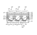
2,102 フォトダイオード部
3,103 電荷転送ゲート
4,4a,4b,104 フローティングディフュージョン部
5,105 増幅用トランジスタ
6,106 垂直選択用トランジスタ
7,107 リセットトランジスタ
8,108 電源線
9,109 読み出し信号線
10,20,30,100 単位画素
11 垂直シフトレジスタ
12 水平シフトレジスタ
13 垂直選択線
14 垂直リセット線
15 垂直信号線
16 水平選択用トランジスタ
17 水平選択線
18 水平信号線
24,124 絶縁層
25,125 パッシベーション膜
26 画素色フィルタ層
27 オンチップレンズ
28 FD部を共有し合う単位画素間の境界位置
29 FD部を共有しない単位画素間の境界位置
31 j行Grとj+1行Bのフォトダイオード重心距離
32 j行Rとj+1行Gbのフォトダイオード重心距離
33 j行Grとj+1行Gbのフォトダイオード重心距離
34 j+1行Gbとj+2行Grのフォトダイオード重心距離
35 j+1行Bとj+2行Grのフォトダイオード重心距離
36 j+1行Gbとj+2行Rのフォトダイオード重心距離
37 j行Rとj+1行Bのフォトダイオード重心距離
38 j+1行Bとj+2行Rのフォトダイオード重心距離
41 i列Grとi+1列Rのフォトダイオード重心距離
42 i列Bとi+1列Gbのフォトダイオード重心距離
43 i列Grとi+1列Gbのフォトダイオード重心距離
44 i+1列Gbとi+2列Grのフォトダイオード重心距離
45 i+1列Rとi+2列Grのフォトダイオード重心距離
46 j+1列Gbとj+2列Rのフォトダイオード重心距離
51 共有画素
61 画素ピッチA
62 画素ピッチB
121 1層目の配線
122 2層目の配線
123 3層目の配線
126 画素色フィルタ層
127 オンチップレンズ
Claims (2)
- 半導体基板上に、光を信号電荷に変換して蓄積するフォトダイオードが行列状(i,j)に複数配置され、前記フォトダイオードに蓄積された前記信号電荷を読み出すための電荷転送ゲートと、前記電荷転送ゲートを介して読み出した前記フォトダイオードで光電変換された前記信号電荷を電位に変換するフローティングディフュージョンとが設けられ、前記信号電荷をリセットするリセットトランジスタ及び読出した信号電荷を増幅する増幅用トランジスタを複数の前記フォトダイオードで共有する固体撮像装置において、
前記リセットトランジスタと前記増幅用トランジスタとを共有する共有領域内の第1フォトダイオード(i,j)と第2フォトダイオード(i,j+1)の間に配置された前記リセットトランジスタ又は前記増幅用トランジスタの一方を備え、
前記第1フォトダイオード(i,j)と第2フォトダイオード(i,j+1)の間に配置されていない他方の前記リセットトランジスタ又は前記増幅用トランジスタが、第3フォトダイオード(i+1,j+n)と第4フォトダイオード(i+1,j+n+1)の間に配置され、かつ
前記nが−1又は+1であることを特徴とする固体撮像装置。 - 半導体基板上に、光を信号電荷に変換して蓄積するフォトダイオードが行列状(i,j)に複数配置され、前記フォトダイオードに蓄積された前記信号電荷を読み出すための電荷転送ゲートと、前記電荷転送ゲートを介して読み出した前記フォトダイオードで光電変換された前記信号電荷を電位に変換するフローティングディフュージョンとが設けられ、前記信号電荷をリセットするリセットトランジスタ及び読出した信号電荷を増幅する増幅用トランジスタを複数のフォトダイオードで共有する固体撮像装置において、
前記リセットトランジスタ、前記増幅用トランジスタを共有する共有領域内の第1フォトダイオード(i,j)と第2フォトダイオード(i+1,j)の間に配置された前記リセットトランジスタ又は前記増幅用トランジスタの一方を備え、
前記第1フォトダイオード(i,j)と第2フォトダイオード(i+1,j)の間に配置されていない他方の前記リセットトランジスタ又は前記増幅用トランジスタが、第3フォトダイオード(i+n,j+1)と第4フォトダイオード(i+n+1,j+1)の間に配置され、かつ
前記nが−1又は+1であることを特徴とする固体撮像装置。
Priority Applications (1)
| Application Number | Priority Date | Filing Date | Title |
|---|---|---|---|
| JP2009245346A JP4457325B2 (ja) | 2007-04-18 | 2009-10-26 | 固体撮像装置 |
Applications Claiming Priority (2)
| Application Number | Priority Date | Filing Date | Title |
|---|---|---|---|
| JP2007108869 | 2007-04-18 | ||
| JP2009245346A JP4457325B2 (ja) | 2007-04-18 | 2009-10-26 | 固体撮像装置 |
Related Parent Applications (1)
| Application Number | Title | Priority Date | Filing Date |
|---|---|---|---|
| JP2009511829A Division JP4457326B2 (ja) | 2007-04-18 | 2008-04-16 | 固体撮像装置 |
Publications (2)
| Publication Number | Publication Date |
|---|---|
| JP2010063120A JP2010063120A (ja) | 2010-03-18 |
| JP4457325B2 true JP4457325B2 (ja) | 2010-04-28 |
Family
ID=39925602
Family Applications (2)
| Application Number | Title | Priority Date | Filing Date |
|---|---|---|---|
| JP2009511829A Expired - Fee Related JP4457326B2 (ja) | 2007-04-18 | 2008-04-16 | 固体撮像装置 |
| JP2009245346A Expired - Fee Related JP4457325B2 (ja) | 2007-04-18 | 2009-10-26 | 固体撮像装置 |
Family Applications Before (1)
| Application Number | Title | Priority Date | Filing Date |
|---|---|---|---|
| JP2009511829A Expired - Fee Related JP4457326B2 (ja) | 2007-04-18 | 2008-04-16 | 固体撮像装置 |
Country Status (4)
| Country | Link |
|---|---|
| US (1) | US8208054B2 (ja) |
| JP (2) | JP4457326B2 (ja) |
| KR (1) | KR101068698B1 (ja) |
| WO (1) | WO2008133146A1 (ja) |
Cited By (1)
| Publication number | Priority date | Publication date | Assignee | Title |
|---|---|---|---|---|
| US8860100B2 (en) | 2010-12-10 | 2014-10-14 | Seiko Epson Corporation | Solid-state imaging device |
Families Citing this family (26)
| Publication number | Priority date | Publication date | Assignee | Title |
|---|---|---|---|---|
| JP5584982B2 (ja) | 2009-02-09 | 2014-09-10 | ソニー株式会社 | 固体撮像素子およびカメラシステム |
| US8059222B2 (en) * | 2007-07-19 | 2011-11-15 | Sharp Kabushiki Kaisha | Display device and method for manufacturing the same |
| GB2466213B (en) * | 2008-12-12 | 2013-03-06 | Cmosis Nv | Pixel array with shared readout circuitry |
| JP5109962B2 (ja) * | 2008-12-22 | 2012-12-26 | ソニー株式会社 | 固体撮像装置および電子機器 |
| US8576312B2 (en) | 2009-02-04 | 2013-11-05 | Rosnes Corporation | Solid-state image pickup device with particular pixel arrangement |
| WO2010090133A1 (ja) * | 2009-02-04 | 2010-08-12 | 株式会社 Rosnes | 固体撮像装置 |
| US8547458B2 (en) | 2009-02-04 | 2013-10-01 | Rosnes Corporation | Solid-state image pickup device |
| JP4881987B2 (ja) * | 2009-10-06 | 2012-02-22 | キヤノン株式会社 | 固体撮像装置および撮像装置 |
| JP5537172B2 (ja) | 2010-01-28 | 2014-07-02 | ソニー株式会社 | 固体撮像装置及び電子機器 |
| JP5526928B2 (ja) * | 2010-03-30 | 2014-06-18 | ソニー株式会社 | 固体撮像装置および撮像装置 |
| JP5672776B2 (ja) * | 2010-06-02 | 2015-02-18 | ソニー株式会社 | 画像処理装置、および画像処理方法、並びにプログラム |
| JP5697371B2 (ja) | 2010-07-07 | 2015-04-08 | キヤノン株式会社 | 固体撮像装置および撮像システム |
| JP5885401B2 (ja) | 2010-07-07 | 2016-03-15 | キヤノン株式会社 | 固体撮像装置および撮像システム |
| JP5751766B2 (ja) * | 2010-07-07 | 2015-07-22 | キヤノン株式会社 | 固体撮像装置および撮像システム |
| JP5656484B2 (ja) | 2010-07-07 | 2015-01-21 | キヤノン株式会社 | 固体撮像装置および撮像システム |
| JP5643555B2 (ja) | 2010-07-07 | 2014-12-17 | キヤノン株式会社 | 固体撮像装置及び撮像システム |
| JP5646421B2 (ja) * | 2011-09-22 | 2014-12-24 | 株式会社東芝 | 固体撮像装置および固体撮像システム |
| JP2014090088A (ja) * | 2012-10-30 | 2014-05-15 | Renesas Electronics Corp | 半導体装置およびその製造方法 |
| US9502457B2 (en) * | 2015-01-29 | 2016-11-22 | Semiconductor Components Industries, Llc | Global shutter image sensor pixels having centralized charge storage regions |
| JP2017042708A (ja) * | 2015-08-26 | 2017-03-02 | セイコーエプソン株式会社 | 液滴吐出方法、プログラム、有機el装置の製造方法、カラーフィルターの形成方法 |
| JP2020113573A (ja) * | 2019-01-08 | 2020-07-27 | キヤノン株式会社 | 光電変換装置 |
| JP2020115516A (ja) * | 2019-01-17 | 2020-07-30 | ソニーセミコンダクタソリューションズ株式会社 | 撮像装置 |
| US20230290791A1 (en) * | 2020-08-07 | 2023-09-14 | Rosnes Corporation | Imaging device |
| US20230308780A1 (en) * | 2020-08-21 | 2023-09-28 | Rosnes Corporation | Imaging device, and electronic instrument comprising imaging device |
| WO2022067455A1 (en) * | 2020-09-29 | 2022-04-07 | Huawei Technologies Co., Ltd. | Solid state imaging device |
| CN117880653A (zh) * | 2021-12-22 | 2024-04-12 | 荣耀终端有限公司 | 多光谱传感器以及电子设备 |
Citations (3)
| Publication number | Priority date | Publication date | Assignee | Title |
|---|---|---|---|---|
| JP2004215048A (ja) * | 2003-01-07 | 2004-07-29 | Matsushita Electric Ind Co Ltd | 固体撮像装置 |
| JP2005183527A (ja) * | 2003-12-17 | 2005-07-07 | Iwate Toshiba Electronics Co Ltd | Cmosイメージセンサ |
| JP2006080937A (ja) * | 2004-09-10 | 2006-03-23 | Sony Corp | 物理情報取得方法および物理情報取得装置、並びに物理量分布検知の半導体装置、プログラム、および撮像モジュール |
Family Cites Families (7)
| Publication number | Priority date | Publication date | Assignee | Title |
|---|---|---|---|---|
| US6043478A (en) | 1998-06-25 | 2000-03-28 | Industrial Technology Research Institute | Active pixel sensor with shared readout structure |
| JP4221940B2 (ja) | 2002-03-13 | 2009-02-12 | ソニー株式会社 | 固体撮像素子及び固体撮像装置並びに撮像システム |
| JP3794637B2 (ja) * | 2003-03-07 | 2006-07-05 | 松下電器産業株式会社 | 固体撮像装置 |
| JP2005198001A (ja) | 2004-01-07 | 2005-07-21 | Canon Inc | 固体撮像装置 |
| JP4793042B2 (ja) | 2005-03-24 | 2011-10-12 | ソニー株式会社 | 固体撮像素子及び撮像装置 |
| TW200742425A (en) * | 2006-03-24 | 2007-11-01 | Matsushita Electric Ind Co Ltd | Solid-state image pickup device |
| US7902618B2 (en) * | 2008-11-17 | 2011-03-08 | Omni Vision Technologies, Inc. | Backside illuminated imaging sensor with improved angular response |
-
2008
- 2008-04-16 US US12/595,229 patent/US8208054B2/en active Active
- 2008-04-16 KR KR1020097020084A patent/KR101068698B1/ko not_active IP Right Cessation
- 2008-04-16 JP JP2009511829A patent/JP4457326B2/ja not_active Expired - Fee Related
- 2008-04-16 WO PCT/JP2008/057439 patent/WO2008133146A1/ja active Application Filing
-
2009
- 2009-10-26 JP JP2009245346A patent/JP4457325B2/ja not_active Expired - Fee Related
Patent Citations (3)
| Publication number | Priority date | Publication date | Assignee | Title |
|---|---|---|---|---|
| JP2004215048A (ja) * | 2003-01-07 | 2004-07-29 | Matsushita Electric Ind Co Ltd | 固体撮像装置 |
| JP2005183527A (ja) * | 2003-12-17 | 2005-07-07 | Iwate Toshiba Electronics Co Ltd | Cmosイメージセンサ |
| JP2006080937A (ja) * | 2004-09-10 | 2006-03-23 | Sony Corp | 物理情報取得方法および物理情報取得装置、並びに物理量分布検知の半導体装置、プログラム、および撮像モジュール |
Cited By (1)
| Publication number | Priority date | Publication date | Assignee | Title |
|---|---|---|---|---|
| US8860100B2 (en) | 2010-12-10 | 2014-10-14 | Seiko Epson Corporation | Solid-state imaging device |
Also Published As
| Publication number | Publication date |
|---|---|
| JPWO2008133146A1 (ja) | 2010-07-22 |
| KR101068698B1 (ko) | 2011-09-28 |
| JP4457326B2 (ja) | 2010-04-28 |
| WO2008133146A1 (ja) | 2008-11-06 |
| US8208054B2 (en) | 2012-06-26 |
| US20100066877A1 (en) | 2010-03-18 |
| KR20090125143A (ko) | 2009-12-03 |
| JP2010063120A (ja) | 2010-03-18 |
Similar Documents
| Publication | Publication Date | Title |
|---|---|---|
| JP4457325B2 (ja) | 固体撮像装置 | |
| JP7264187B2 (ja) | 固体撮像装置およびその駆動方法、並びに電子機器 | |
| US20200176498A1 (en) | Solid-state imaging device and method of manufacturing the same, and imaging apparatus | |
| KR101129128B1 (ko) | 후면 조사 이미지 센서를 위한 회로 및 광센서 오버랩 | |
| JP5290923B2 (ja) | 固体撮像装置および撮像装置 | |
| JP4793042B2 (ja) | 固体撮像素子及び撮像装置 | |
| US20140184808A1 (en) | Photoelectric Conversion Device and Imaging Apparatus Having the Photoelectric Conversion Device | |
| JP6026102B2 (ja) | 固体撮像素子および電子機器 | |
| JP4341664B2 (ja) | 固体撮像装置および撮像装置 | |
| JP5629995B2 (ja) | 撮像素子および撮像装置 | |
| JP2010130657A (ja) | 固体撮像装置及びそれを用いた撮像システム | |
| JP2009088255A (ja) | カラー固体撮像装置および電子情報機器 | |
| JP2016058818A (ja) | 撮像装置及び撮像システム | |
| JP2011029291A (ja) | 固体撮像装置及びカメラ | |
| JP4700947B2 (ja) | 光電変換膜積層型単板式カラー固体撮像装置 | |
| JP5789446B2 (ja) | Mos型固体撮像素子及び撮像装置 | |
| JP5216259B2 (ja) | 固体撮像素子および撮像装置 | |
| JP4495949B2 (ja) | 2板式カラー固体撮像装置及びデジタルカメラ | |
| JP2005340572A (ja) | 光電変換膜積層型固体撮像装置 | |
| WO2010090133A1 (ja) | 固体撮像装置 | |
| JP2007066962A (ja) | カラー固体撮像装置及びデジタルカメラ | |
| JP2004186311A (ja) | Mos型イメージセンサ及びデジタルカメラ | |
| JP2006165663A (ja) | 撮像装置、デジタルカメラ、及びカラー画像データ生成方法 | |
| JP4491352B2 (ja) | 固体撮像素子 | |
| JP2005175893A (ja) | 2板式カラー固体撮像装置及びデジタルカメラ |
Legal Events
| Date | Code | Title | Description |
|---|---|---|---|
| A975 | Report on accelerated examination |
Free format text: JAPANESE INTERMEDIATE CODE: A971005 Effective date: 20091208 |
|
| TRDD | Decision of grant or rejection written | ||
| A01 | Written decision to grant a patent or to grant a registration (utility model) |
Free format text: JAPANESE INTERMEDIATE CODE: A01 Effective date: 20100105 |
|
| A01 | Written decision to grant a patent or to grant a registration (utility model) |
Free format text: JAPANESE INTERMEDIATE CODE: A01 |
|
| A61 | First payment of annual fees (during grant procedure) |
Free format text: JAPANESE INTERMEDIATE CODE: A61 Effective date: 20100127 |
|
| R150 | Certificate of patent or registration of utility model |
Ref document number: 4457325 Country of ref document: JP Free format text: JAPANESE INTERMEDIATE CODE: R150 Free format text: JAPANESE INTERMEDIATE CODE: R150 |
|
| FPAY | Renewal fee payment (event date is renewal date of database) |
Free format text: PAYMENT UNTIL: 20130219 Year of fee payment: 3 |
|
| FPAY | Renewal fee payment (event date is renewal date of database) |
Free format text: PAYMENT UNTIL: 20130219 Year of fee payment: 3 |
|
| FPAY | Renewal fee payment (event date is renewal date of database) |
Free format text: PAYMENT UNTIL: 20130219 Year of fee payment: 3 |
|
| FPAY | Renewal fee payment (event date is renewal date of database) |
Free format text: PAYMENT UNTIL: 20140219 Year of fee payment: 4 |
|
| R250 | Receipt of annual fees |
Free format text: JAPANESE INTERMEDIATE CODE: R250 |
|
| R250 | Receipt of annual fees |
Free format text: JAPANESE INTERMEDIATE CODE: R250 |
|
| R250 | Receipt of annual fees |
Free format text: JAPANESE INTERMEDIATE CODE: R250 |
|
| R250 | Receipt of annual fees |
Free format text: JAPANESE INTERMEDIATE CODE: R250 |
|
| R250 | Receipt of annual fees |
Free format text: JAPANESE INTERMEDIATE CODE: R250 |
|
| R250 | Receipt of annual fees |
Free format text: JAPANESE INTERMEDIATE CODE: R250 |
|
| R250 | Receipt of annual fees |
Free format text: JAPANESE INTERMEDIATE CODE: R250 |
|
| R250 | Receipt of annual fees |
Free format text: JAPANESE INTERMEDIATE CODE: R250 |
|
| LAPS | Cancellation because of no payment of annual fees |