JP4366192B2 - 超小型電子加工物の電気化学機械処理の方法及び装置 - Google Patents
超小型電子加工物の電気化学機械処理の方法及び装置 Download PDFInfo
- Publication number
- JP4366192B2 JP4366192B2 JP2003574388A JP2003574388A JP4366192B2 JP 4366192 B2 JP4366192 B2 JP 4366192B2 JP 2003574388 A JP2003574388 A JP 2003574388A JP 2003574388 A JP2003574388 A JP 2003574388A JP 4366192 B2 JP4366192 B2 JP 4366192B2
- Authority
- JP
- Japan
- Prior art keywords
- workpiece
- electrode
- remote
- electrodes
- carried
- Prior art date
- Legal status (The legal status is an assumption and is not a legal conclusion. Google has not performed a legal analysis and makes no representation as to the accuracy of the status listed.)
- Expired - Fee Related
Links
Images


Classifications
-
- B—PERFORMING OPERATIONS; TRANSPORTING
- B24—GRINDING; POLISHING
- B24B—MACHINES, DEVICES, OR PROCESSES FOR GRINDING OR POLISHING; DRESSING OR CONDITIONING OF ABRADING SURFACES; FEEDING OF GRINDING, POLISHING, OR LAPPING AGENTS
- B24B37/00—Lapping machines or devices; Accessories
- B24B37/04—Lapping machines or devices; Accessories designed for working plane surfaces
- B24B37/042—Lapping machines or devices; Accessories designed for working plane surfaces operating processes therefor
-
- H—ELECTRICITY
- H01—ELECTRIC ELEMENTS
- H01L—SEMICONDUCTOR DEVICES NOT COVERED BY CLASS H10
- H01L21/00—Processes or apparatus adapted for the manufacture or treatment of semiconductor or solid state devices or of parts thereof
- H01L21/02—Manufacture or treatment of semiconductor devices or of parts thereof
- H01L21/04—Manufacture or treatment of semiconductor devices or of parts thereof the devices having at least one potential-jump barrier or surface barrier, e.g. PN junction, depletion layer or carrier concentration layer
- H01L21/18—Manufacture or treatment of semiconductor devices or of parts thereof the devices having at least one potential-jump barrier or surface barrier, e.g. PN junction, depletion layer or carrier concentration layer the devices having semiconductor bodies comprising elements of Group IV of the Periodic System or AIIIBV compounds with or without impurities, e.g. doping materials
- H01L21/30—Treatment of semiconductor bodies using processes or apparatus not provided for in groups H01L21/20 - H01L21/26
- H01L21/302—Treatment of semiconductor bodies using processes or apparatus not provided for in groups H01L21/20 - H01L21/26 to change their surface-physical characteristics or shape, e.g. etching, polishing, cutting
- H01L21/304—Mechanical treatment, e.g. grinding, polishing, cutting
-
- B—PERFORMING OPERATIONS; TRANSPORTING
- B23—MACHINE TOOLS; METAL-WORKING NOT OTHERWISE PROVIDED FOR
- B23H—WORKING OF METAL BY THE ACTION OF A HIGH CONCENTRATION OF ELECTRIC CURRENT ON A WORKPIECE USING AN ELECTRODE WHICH TAKES THE PLACE OF A TOOL; SUCH WORKING COMBINED WITH OTHER FORMS OF WORKING OF METAL
- B23H5/00—Combined machining
- B23H5/06—Electrochemical machining combined with mechanical working, e.g. grinding or honing
- B23H5/08—Electrolytic grinding
-
- B—PERFORMING OPERATIONS; TRANSPORTING
- B23—MACHINE TOOLS; METAL-WORKING NOT OTHERWISE PROVIDED FOR
- B23H—WORKING OF METAL BY THE ACTION OF A HIGH CONCENTRATION OF ELECTRIC CURRENT ON A WORKPIECE USING AN ELECTRODE WHICH TAKES THE PLACE OF A TOOL; SUCH WORKING COMBINED WITH OTHER FORMS OF WORKING OF METAL
- B23H5/00—Combined machining
- B23H5/10—Electrodes specially adapted therefor or their manufacture
-
- B—PERFORMING OPERATIONS; TRANSPORTING
- B24—GRINDING; POLISHING
- B24B—MACHINES, DEVICES, OR PROCESSES FOR GRINDING OR POLISHING; DRESSING OR CONDITIONING OF ABRADING SURFACES; FEEDING OF GRINDING, POLISHING, OR LAPPING AGENTS
- B24B37/00—Lapping machines or devices; Accessories
- B24B37/04—Lapping machines or devices; Accessories designed for working plane surfaces
-
- B—PERFORMING OPERATIONS; TRANSPORTING
- B24—GRINDING; POLISHING
- B24B—MACHINES, DEVICES, OR PROCESSES FOR GRINDING OR POLISHING; DRESSING OR CONDITIONING OF ABRADING SURFACES; FEEDING OF GRINDING, POLISHING, OR LAPPING AGENTS
- B24B49/00—Measuring or gauging equipment for controlling the feed movement of the grinding tool or work; Arrangements of indicating or measuring equipment, e.g. for indicating the start of the grinding operation
- B24B49/10—Measuring or gauging equipment for controlling the feed movement of the grinding tool or work; Arrangements of indicating or measuring equipment, e.g. for indicating the start of the grinding operation involving electrical means
-
- C—CHEMISTRY; METALLURGY
- C25—ELECTROLYTIC OR ELECTROPHORETIC PROCESSES; APPARATUS THEREFOR
- C25D—PROCESSES FOR THE ELECTROLYTIC OR ELECTROPHORETIC PRODUCTION OF COATINGS; ELECTROFORMING; APPARATUS THEREFOR
- C25D17/00—Constructional parts, or assemblies thereof, of cells for electrolytic coating
- C25D17/001—Apparatus specially adapted for electrolytic coating of wafers, e.g. semiconductors or solar cells
-
- C—CHEMISTRY; METALLURGY
- C25—ELECTROLYTIC OR ELECTROPHORETIC PROCESSES; APPARATUS THEREFOR
- C25D—PROCESSES FOR THE ELECTROLYTIC OR ELECTROPHORETIC PRODUCTION OF COATINGS; ELECTROFORMING; APPARATUS THEREFOR
- C25D7/00—Electroplating characterised by the article coated
- C25D7/12—Semiconductors
- C25D7/123—Semiconductors first coated with a seed layer or a conductive layer
-
- C—CHEMISTRY; METALLURGY
- C25—ELECTROLYTIC OR ELECTROPHORETIC PROCESSES; APPARATUS THEREFOR
- C25F—PROCESSES FOR THE ELECTROLYTIC REMOVAL OF MATERIALS FROM OBJECTS; APPARATUS THEREFOR
- C25F3/00—Electrolytic etching or polishing
- C25F3/16—Polishing
-
- C—CHEMISTRY; METALLURGY
- C25—ELECTROLYTIC OR ELECTROPHORETIC PROCESSES; APPARATUS THEREFOR
- C25F—PROCESSES FOR THE ELECTROLYTIC REMOVAL OF MATERIALS FROM OBJECTS; APPARATUS THEREFOR
- C25F7/00—Constructional parts, or assemblies thereof, of cells for electrolytic removal of material from objects; Servicing or operating
-
- H—ELECTRICITY
- H01—ELECTRIC ELEMENTS
- H01L—SEMICONDUCTOR DEVICES NOT COVERED BY CLASS H10
- H01L21/00—Processes or apparatus adapted for the manufacture or treatment of semiconductor or solid state devices or of parts thereof
- H01L21/02—Manufacture or treatment of semiconductor devices or of parts thereof
- H01L21/04—Manufacture or treatment of semiconductor devices or of parts thereof the devices having at least one potential-jump barrier or surface barrier, e.g. PN junction, depletion layer or carrier concentration layer
- H01L21/18—Manufacture or treatment of semiconductor devices or of parts thereof the devices having at least one potential-jump barrier or surface barrier, e.g. PN junction, depletion layer or carrier concentration layer the devices having semiconductor bodies comprising elements of Group IV of the Periodic System or AIIIBV compounds with or without impurities, e.g. doping materials
- H01L21/30—Treatment of semiconductor bodies using processes or apparatus not provided for in groups H01L21/20 - H01L21/26
- H01L21/31—Treatment of semiconductor bodies using processes or apparatus not provided for in groups H01L21/20 - H01L21/26 to form insulating layers thereon, e.g. for masking or by using photolithographic techniques; After treatment of these layers; Selection of materials for these layers
- H01L21/3205—Deposition of non-insulating-, e.g. conductive- or resistive-, layers on insulating layers; After-treatment of these layers
- H01L21/321—After treatment
- H01L21/32115—Planarisation
- H01L21/3212—Planarisation by chemical mechanical polishing [CMP]
- H01L21/32125—Planarisation by chemical mechanical polishing [CMP] by simultaneously passing an electrical current, i.e. electrochemical mechanical polishing, e.g. ECMP
-
- C—CHEMISTRY; METALLURGY
- C25—ELECTROLYTIC OR ELECTROPHORETIC PROCESSES; APPARATUS THEREFOR
- C25D—PROCESSES FOR THE ELECTROLYTIC OR ELECTROPHORETIC PRODUCTION OF COATINGS; ELECTROFORMING; APPARATUS THEREFOR
- C25D17/00—Constructional parts, or assemblies thereof, of cells for electrolytic coating
- C25D17/10—Electrodes, e.g. composition, counter electrode
- C25D17/14—Electrodes, e.g. composition, counter electrode for pad-plating
-
- C—CHEMISTRY; METALLURGY
- C25—ELECTROLYTIC OR ELECTROPHORETIC PROCESSES; APPARATUS THEREFOR
- C25D—PROCESSES FOR THE ELECTROLYTIC OR ELECTROPHORETIC PRODUCTION OF COATINGS; ELECTROFORMING; APPARATUS THEREFOR
- C25D5/00—Electroplating characterised by the process; Pretreatment or after-treatment of workpieces
- C25D5/04—Electroplating with moving electrodes
- C25D5/06—Brush or pad plating
-
- C—CHEMISTRY; METALLURGY
- C25—ELECTROLYTIC OR ELECTROPHORETIC PROCESSES; APPARATUS THEREFOR
- C25D—PROCESSES FOR THE ELECTROLYTIC OR ELECTROPHORETIC PRODUCTION OF COATINGS; ELECTROFORMING; APPARATUS THEREFOR
- C25D5/00—Electroplating characterised by the process; Pretreatment or after-treatment of workpieces
- C25D5/18—Electroplating using modulated, pulsed or reversing current
-
- C—CHEMISTRY; METALLURGY
- C25—ELECTROLYTIC OR ELECTROPHORETIC PROCESSES; APPARATUS THEREFOR
- C25D—PROCESSES FOR THE ELECTROLYTIC OR ELECTROPHORETIC PRODUCTION OF COATINGS; ELECTROFORMING; APPARATUS THEREFOR
- C25D5/00—Electroplating characterised by the process; Pretreatment or after-treatment of workpieces
- C25D5/22—Electroplating combined with mechanical treatment during the deposition
Description
本出願は、2000年8月30日出願の「超小型電子基板から導電材料を除去する方法及び装置」という名称の米国特許出願第09/651,779号、2001年6月21日出願の「超小型電子基板から導電材料を電気的、機械的、及び/又は化学的に除去する方法及び装置」という名称の米国特許出願第09/888,084号、及び2001年6月21日出願の「隅部が尖っていない装置と共に導電材料を有する超小型電子基板及び導電材料を除去する関連方法」という名称の米国特許出願第09/887,767号の一部継続出願であり、それらは、全て本明細書においてその全内容が引用により組み込まれる。
以下の開示内容は、電気化学機械処理を使用して材料を超小型電子加工物にメッキし、材料を加工物から除去する方法及び装置に関する。
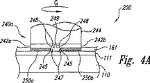
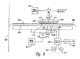
110 超小型電子加工物
113 加工物の処理側
120 加工物ホルダ
130 加工物用電極
142 加工物用電極
142a 第1の遠隔電極
142b 第2の遠隔電極
172 DC電源
174 AC電源
180 スイッチング組立体
Claims (42)
- 超小型電子加工物の電気化学的機械研磨処理のための装置であって、
超小型電子加工物を受け取るように構成された加工物ホルダと、
前記加工物が前記加工物ホルダに受け取られた時に該加工物の処理面と接触するように構成された加工物用電極と、
前記加工物ホルダから間隔を空けて配置された第1の遠隔電極及び第2の遠隔電極と、 前記加工物ホルダに面する支持面と前記第1及び第2の遠隔電極に面する裏側とを有する機械的研磨用の機械的媒体と、
前記加工物用電極、前記第1の遠隔電極、及び前記第2の遠隔電極に結合されたスイッチング組立体と、
前記スイッチング組立体に電気的に結合され、該スイッチング組立体を介して前記第1及び第2の遠隔電極と電気的に連通するAC電源と、
前記スイッチング組立体に電気的に結合され、該スイッチング組立体を介して、前記加工物用電極とある極性で、前記第1及び第2の遠隔電極の少なくとも一方と反対の極性で電気的に連通するDC電源と、
を含むことを特徴とする装置。 - 前記加工物用電極は、前記加工物ホルダによって担持されることを特徴とする請求項1に記載の装置。
- 前記加工物用電極は、前記加工物ホルダによって担持され、
前記第1の遠隔電極及び前記第2の遠隔電極は、前記加工物ホルダとは別の遠隔電極組立体によって担持される、
ことを特徴とする請求項1に記載の装置。 - 前記加工物ホルダは、前記処理面が下を向くように前記加工物を保持する構成を有するチャックを備えた基板キャリアと、該基板キャリアを移動させるために該基板キャリアに結合された駆動組立体とを含み、
前記加工物用電極は、前記加工物ホルダによって担持される、
ことを特徴とする請求項1に記載の装置。 - 前記加工物ホルダは、前記処理面が上を向くように前記加工物を保持する構成を有するチャックを備えた基板キャリアと、該基板キャリアを移動させるために該基板キャリアに結合された駆動組立体とを含み、
前記加工物用電極は、前記加工物ホルダによって担持される、
ことを特徴とする請求項1に記載の装置。 - 前記加工物ホルダから間隔を置いて配置された電極組立体を更に含み、
前記第1の遠隔電極及び前記第2の遠隔電極は、前記電極組立体によって担持される、ことを特徴とする請求項1に記載の装置。 - 前記加工物ホルダから間隔を置いて配置され、該加工物ホルダに対して可動の可動式電極組立体を更に含み、
前記第1の遠隔電極及び前記第2の遠隔電極は、前記電極組立体によって担持される、ことを特徴とする請求項1に記載の装置。 - 前記加工物ホルダから間隔を置いて配置され、該加工物ホルダに対して可動の可動式電極組立体を更に含み、
前記第1の遠隔電極及び前記第2の遠隔電極は、前記電極組立体によって担持され、
前記機械的媒体は、前記第1の遠隔電極によって担持された第1の研磨パッドと、前記第2の遠隔電極によって担持された第2の研磨パッドとを含む、
ことを特徴とする請求項1に記載の装置。 - テーブルを更に含み、
前記機械的媒体は、前記テーブルによって担持された研磨パッドを含み、
前記加工物ホルダは、前記研磨パッドの上に位置決めされ、前記加工物用電極は、該加工物ホルダによって担持され、
前記第1の遠隔電極及び前記第2の遠隔電極は、前記テーブルによって担持される、
ことを特徴とする請求項1に記載の装置。 - (a)前記超小型電子加工物の前記処理面を電気化学処理溶液に接触させる段階と、
(b)前記加工物が前記電気化学処理溶液に接触している間に、前記加工物用電極と前記第1の遠隔電極及び/又は前記第2の遠隔電極の少なくとも一方とに直流電流を印加する段階と、
(c)前記加工物が前記電気化学処理溶液に接触している間に、前記第1の遠隔電極及び/又は前記第2の遠隔電極の少なくとも一方に交流電流を印加する段階と、
(d)少なくとも前記交流電流を印加している間に、前記加工物の前記処理面を前記機械的媒体に押し付ける段階と、
を含む処理に従って装置を作動させるための命令を包含するコンピュータ制御可能媒体を有するコントローラを更に含むことを特徴とする請求項1に記載の装置。 - (a)前記超小型電子加工物の前記処理面を電気化学処理溶液に接触させる段階と、
(b)前記加工物が前記電気化学処理溶液に接触している間に、前記加工物用電極と前記第1の遠隔電極及び/又は前記第2の遠隔電極の少なくとも一方とに直流電流を印加する段階と、
(c)前記加工物が前記電気化学処理溶液に接触している間に、前記第1の遠隔電極及び前記第2の遠隔電極に交流電流を印加する段階と、
(d)少なくとも前記交流電流を印加している間に、前記加工物の前記処理面を前記機械的媒体に押し付ける段階と、
を含む処理に従って装置を作動させるための命令を包含するコンピュータ制御可能媒体を有するコントローラを更に含むことを特徴とする請求項1に記載の装置。 - (a)前記超小型電子加工物の前記処理面を電気化学処理溶液に接触させる段階と、
(b)前記加工物が前記電気化学処理溶液に接触している間に、前記加工物用電極と前記第1の遠隔電極及び/又は前記第2の遠隔電極の少なくとも一方とに直流電流を印加する段階と、
(c)前記直流電流を印加している間に、前記第1の遠隔電極及び前記第2の遠隔電極に交流電流を印加する段階と、
を含む処理に従って装置を作動させるための命令を包含するコンピュータ制御可能媒体を有するコントローラを更に含むことを特徴とする請求項1に記載の装置。 - (a)前記超小型電子加工物の前記処理面を電気化学処理溶液に接触させる段階と、
(b)前記加工物が前記電気化学処理溶液に接触している間に、前記加工物用電極と前記第1の遠隔電極及び/又は前記第2の遠隔電極の少なくとも一方とに直流電流を印加する段階と、
(c)前記加工物が前記電気化学処理溶液に接触している間に、前記第1の遠隔電極及び前記第2の遠隔電極に交流電流を印加する段階と、
(d)少なくとも前記交流電流を印加している間に、前記加工物の前記処理面を前記機械的媒体に押し付ける段階と、
(e)前記第1及び第2の遠隔電極の滞留時間が前記加工物の第1の領域で第2の領域よりも長くなるように、該加工物及び/又は該第1及び第2の遠隔電極の少なくとも1つを移動させる段階と、
を含む処理に従って装置を作動させるための命令を包含するコンピュータ制御可能媒体を有するコントローラを更に含むことを特徴とする請求項1に記載の装置。 - 超小型電子加工物の電気化学的機械研磨処理のための装置であって、
超小型電子加工物を受け取るように構成された加工物ホルダと、
前記加工物が前記加工物ホルダに受け取られた時に該加工物の処理面と接触するように構成された加工物用電極と、
前記加工物が前記加工物ホルダに受け取られた時に該加工物の処理面から間隔が空くように該加工物ホルダに並置された第1の遠隔電極及び第2の遠隔電極と、
AC電源と、
DC電源と、
前記加工物用電極、前記第1の遠隔電極、前記第2の遠隔電極、前記AC電源、及び前記DC電源に結合されたスイッチング組立体であって、該スイッチング組立体は少なくとも第1の構成及び第2の構成を含み、該第1の構成では、前記DC電源が前記加工物用電極及び前記第1の遠隔電極に結合されるのに対し、前記AC電源は前記第1及び第2の遠隔電極に同時に結合され、該第2の構成では、前記DC電源が前記加工物用電極及び前記第1及び第2の遠隔電極の両方に結合されるのに対し、前記AC電源は同時に前記第1及び第2の遠隔電極に結合される、前記スイッチング組立体と、
を含むことを特徴とする装置。 - 前記加工物用電極は、前記加工物ホルダによって担持され、
前記加工物ホルダに面する支持面と前記第1及び第2の遠隔電極に面する裏側とを有する機械的研磨用の機械的媒体、
を更に含むことを特徴とする請求項14に記載の装置。 - 前記加工物用電極は、前記加工物ホルダによって担持され、
前記第1の遠隔電極及び前記第2の遠隔電極は、前記加工物ホルダとは別の電極組立体によって担持される、
ことを特徴とする請求項15に記載の装置。 - 前記加工物ホルダから間隔を置いて配置された電極組立体を更に含み、
前記第1及び第2の遠隔電極は、前記電極組立体によって担持される、
ことを特徴とする請求項15に記載の装置。 - 前記加工物ホルダから間隔を置いて配置され、該加工物ホルダに対して可動の可動式電極組立体を更に含み、
前記第1及び第2の遠隔電極は、前記電極組立体によって担持される、
ことを特徴とする請求項15に記載の装置。 - 前記加工物ホルダから間隔を置いて配置された可動式電極組立体を更に含み、
前記第1及び第2の遠隔電極は、前記電極組立体によって担持され、
前記機械的媒体は、前記第1の遠隔電極によって担持された第1の研磨パッドと、前記第2の遠隔電極によって担持された第2の研磨パッドとを含む、
ことを特徴とする請求項15に記載の装置。 - テーブルを更に含み、
前記機械的媒体は、前記テーブルによって担持された研磨パッドを含み、
前記加工物ホルダは、前記研磨パッドの上に位置決めされ、前記加工物用電極は、該加工物ホルダによって担持され、
前記第1及び第2の遠隔電極は、前記テーブルによって担持される、
ことを特徴とする請求項15に記載の装置。 - 超小型電子加工物の電気化学的機械研磨処理のための装置であって、
超小型電子加工物を受け取るように構成された加工物ホルダと、
前記加工物が前記加工物ホルダに受け取られた時に該加工物の処理面に接触するように構成された第1の電極と、
前記加工物ホルダから間隔の空いた遠隔電極である第2の電極及び第3の電極と、
前記加工物ホルダと前記第2及び第3の電極の各々との間の機械的研磨用の機械的媒体と、
AC電源と、
DC電源と、
前記第1の電極、第2の電極、第3の電極、AC電源、及びDC電源に結合されたスイッチング組立体であって、該スイッチング組立体は、次の少なくとも3つの構成:
前記DC電源が前記加工物用電極及び前記第1及び第2の遠隔電極から切断されるのに対し、前記AC電源は前記第1及び第2の遠隔電極に結合される、第1の構成;
前記DC電源が前記加工物用電極及び前記第1及び第2の両方の遠隔電極に結合されるのに対し、前記AC電源は前記第1及び第2の遠隔電極から切断される、第2の構成;及び、
前記DC電源が前記加工物用電極及び前記第1及び第2の両方の遠隔電極に結合されるのに対し、前記AC電源は同時に前記第1及び第2の遠隔電極に結合される、第3の構成;
を含む、前記スイッチング組立体と、
を含むことを特徴とする装置。 - 前記第1の電極は、前記加工物ホルダによって担持されることを特徴とする請求項21に記載の装置。
- 前記第1の電極は、前記加工物ホルダによって担持され、
前記第2及び第3の電極は、前記加工物ホルダとは別の電極組立体によって担持される、
ことを特徴とする請求項21に記載の装置。 - 前記加工物ホルダは、前記処理面が下を向くように前記加工物を保持する構成を有するチャックを備えた基板キャリアと、該基板キャリアを移動させるために該基板キャリアに結合された駆動組立体とを含み、
前記第1の電極は、前記加工物ホルダによって担持される、
ことを特徴とする請求項21に記載の装置。 - 前記加工物ホルダは、前記処理面が上を向くように前記加工物を保持する構成を有するチャックを備えた基板キャリアと、該基板キャリアを移動させるために該基板キャリアに結合された駆動組立体とを含み、
前記第1の電極は、前記加工物ホルダによって担持される、
ことを特徴とする請求項21に記載の装置。 - 前記加工物ホルダから間隔を置いて配置された電極組立体を更に含み、
前記第2及び第3の電極は、前記電極組立体によって担持される、
ことを特徴とする請求項21に記載の装置。 - 前記加工物ホルダから間隔を置いて配置された可動式電極組立体を更に含み、
前記第2及び第3の電極は、前記電極組立体によって担持される、
ことを特徴とする請求項21に記載の装置。 - 前記加工物ホルダから間隔を置いて配置された可動式電極組立体を更に含み、
前記第2及び第3の電極は、前記電極組立体によって担持され、
前記機械的媒体は、前記第2の電極によって担持された第1の研磨パッドと、前記第3の電極によって担持された第2の研磨パッドとを含む、
ことを特徴とする請求項21に記載の装置。 - テーブルを更に含み、
前記機械的媒体は、前記テーブルによって担持された研磨パッドを含み、
前記加工物ホルダは、前記研磨パッドの上に位置決めされ、前記第1の電極は、該加工物ホルダによって担持され、
前記第2及び第3の電極は、前記テーブルによって担持される、
ことを特徴とする請求項21に記載の装置。 - (a)前記超小型電子加工物の前記処理面を電解液に接触させる段階と、
(b)前記加工物が前記電解液に接触している間に、前記第1の電極と前記第2及び/又は前記第3の電極の少なくとも一方に直流電流を印加する段階と、
(c)前記加工物が前記電解液に接触している間に、前記第2及び/又は前記第3の電極の少なくとも一方に交流電流を印加する段階と、
(d)少なくとも前記交流電流を印加している間に、前記加工物の前記処理面を前記機械的媒体に押し付ける段階と、
を含む処理に従って装置を作動させるための命令を包含するコンピュータ制御可能媒体を有するコントローラを更に含むことを特徴とする請求項21に記載の装置。 - (a)前記超小型電子加工物の前記処理面を電解液に接触させる段階と、
(b)前記加工物が前記電解液に接触している間に、前記第1の電極と前記第2及び/又は前記第3の電極の少なくとも一方に直流電流を印加する段階と、
(c)前記加工物が前記電解液に接触している間に、前記第2及び第3の電極に交流電流を印加する段階と、
(d)少なくとも前記交流電流を印加している間に、前記加工物の前記処理面を前記機械的媒体に押し付ける段階と、
を含む処理に従って装置を作動させるための命令を包含するコンピュータ制御可能媒体を有するコントローラを更に含むことを特徴とする請求項21に記載の装置。 - (a)前記超小型電子加工物の前記処理面を電解液に接触させる段階と、
(b)前記加工物が前記電解液に接触している間に、前記第1の電極と前記第2及び/又は前記第3の電極の少なくとも一方に直流電流を印加する段階と、
(c)前記直流電流を印加している間に、前記第2及び第3の電極に交流電流を印加する段階と、
を含む処理に従って装置を作動させるための命令を包含するコンピュータ制御可能媒体を有するコントローラを更に含むことを特徴とする請求項21に記載の装置。 - (a)前記超小型電子加工物の前記処理面を電解液に接触させる段階と、
(b)前記加工物が前記電解液に接触している間に、前記第1の電極と前記第2及び/又は前記第3の電極の少なくとも一方に直流電流を印加する段階と、
(c)前記加工物が前記電解液に接触している間に、前記第2及び第3の電極に交流電流を印加する段階と、
(d)少なくとも前記交流電流を印加している間に、前記加工物の前記処理面を前記機械的媒体に押し付ける段階と、
(e)前記第2及び第3の電極の滞留時間が前記加工物の第1の領域で第2の領域よりも長くなるように、該加工物及び/又は該第2及び第3の電極の少なくとも1つを移動させる段階と、
を含む処理に従って装置を作動させるための命令を包含するコンピュータ制御可能媒体を有するコントローラを更に含むことを特徴とする請求項21に記載の装置。 - 超小型電子加工物の電気化学的機械研磨処理のための装置であって、
超小型電子加工物を受け取るように構成された加工物ホルダと、
前記加工物が前記加工物ホルダに受け取られた時に該加工物の処理面と接触するように構成された加工物用電極と、
前記加工物ホルダから間隔を置いて配置された第1の遠隔電極及び第2の遠隔電極と、 前記加工物ホルダと前記第1及び第2の遠隔電極の各々との間の機械的研磨用の機械的媒体と、
AC電源と、
DC電源と、
前記加工物用電極、第1の遠隔電極、第2の遠隔電極、AC電源、及びDC電源に結合されたスイッチング組立体と、
(a)前記加工物用電極と前記第1及び第2の遠隔電極の少なくとも一方とを前記スイッチング組立体を介して前記DC電源に接続する段階、及び/又は、(b)前記第1及び第2の遠隔電極を前記スイッチング組立体を介して前記交流電源に接続する段階を含む処理に従って前記スイッチング組立体を作動させるための命令を包含するコンピュータ制御可能媒体を含む、該スイッチング組立体に結合されたコントローラと、
を含むことを特徴とする装置。 - 超小型電子加工物の電気化学的機械研磨処理のための装置であって、
超小型電子加工物を受け取るように構成された加工物ホルダと、
前記加工物が前記加工物ホルダに受け取られた時に該加工物の処理面と接触するように構成された加工物用電極と、
前記加工物ホルダから間隔を置いて配置された第1の遠隔電極及び第2の遠隔電極と、 前記加工物ホルダと前記第1及び第2の遠隔電極の各々との間の機械的研磨用の機械的媒体と、
前記加工物用電極、前記第1の遠隔電極、及び前記第2の遠隔電極に結合されたスイッチング組立体と、
前記スイッチング組立体に電気的に結合され、前記第1及び第2の遠隔電極と電気的に連通するAC電源と、
前記スイッチング組立体に電気的に結合され、該スイッチング組立体を介して、前記加工物用電極とある極性で、前記第1及び第2の遠隔電極の少なくとも一方と反対の極性で電気的に連通するDC電源と、
を含むことを特徴とする装置。 - 超小型電子加工物の電気化学的機械研磨処理のための装置であって、
超小型電子加工物を受け取るように構成された加工物ホルダと、
前記加工物が前記加工物ホルダに受け取られた時に該加工物の処理面に接触するように構成され、該加工物ホルダによって担持された加工物用電極と、
前記加工物ホルダに面する電極組立体と、該電極組立体によって担持された第1の遠隔電極と、該電極組立体によって担持された第2の遠隔電極と、該加工物ホルダから間隔を置いて配置された該第1及び第2の遠隔電極によって担持された機械的研磨用の機械的媒体とを含む材料除去装置と、
AC電源と、
DC電源と、
前記加工物用電極、第1の遠隔電極、第2の遠隔電極、AC電源、及びDC電源に結合されたスイッチング組立体であって、該スイッチング組立体は、次の少なくとも3つの構成:
前記DC電源が前記加工物用電極及び前記第1及び第2の遠隔電極から切断されるのに対し、前記AC電源は前記第1及び第2の遠隔電極に結合される、第1の構成;
前記DC電源が前記加工物用電極及び前記第1及び第2の両方の遠隔電極に結合されるのに対し、前記AC電源は前記第1及び第2の遠隔電極から切断される、第2の構成;及び、
前記DC電源が前記加工物用電極及び前記第1及び第2の両方の遠隔電極に結合されるのに対し、前記AC電源は同時に前記第1及び第2の遠隔電極に結合される、第3の構成;
を含む、前記スイッチング組立体と、
を含むことを特徴とする装置。 - 超小型電子加工物の電気化学的機械研磨処理のための装置であって、
超小型電子加工物を受け取るように構成された加工物ホルダと、
前記加工物が前記加工物ホルダに受け取られた時に該加工物の処理面に接触するように構成され、該加工物ホルダによって担持された加工物用電極と、
前記加工物ホルダに面する電極組立体と、該電極組立体によって担持された第1の遠隔電極と、該電極組立体によって担持された第2の遠隔電極と、該第1及び第2の遠隔電極によって担持された機械的研磨用の機械的媒体とを含む材料除去装置と、
を含み、
前記電極組立体は、前記第1及び第2の遠隔電極を前記加工物ホルダに対して移動させるために可動であり、
AC電源と、
DC電源と、
前記加工物用電極、第1の遠隔電極、第2の遠隔電極、AC電源、及びDC電源に結合されたスイッチング組立体であって、該スイッチング組立体は、次の少なくとも2つの構成:
前記DC電源が前記加工物用電極及び前記第1及び第2の遠隔電極に結合されるのに対し、前記AC電源は前記第1の遠隔電極に結合される、第1の構成;及び、
前記DC電源が前記加工物用電極及び前記第2の遠隔電極に結合されるのに対し、前記AC電源は同時に前記第1及び第2の遠隔電極に結合される、第2の構成;
を含む、前記スイッチング組立体と、
を更に含むことを特徴とする装置。 - 超小型電子加工物を電気化学機械的に研磨処理する方法であって、
超小型電子加工物の処理面を電解液に接触させる段階と、
前記加工物の前記処理面に接触し、前記電解液と電気的に連通した加工物用電極と、前記加工物の前記処理面から離隔し、前記電解液と電気的に連通した第1の遠隔電極とに対して直流電流を印加する段階と、
前記電解液と電気的に連通した前記第1の遠隔電極と、前記加工物の前記処理面から離隔し、前記電解液と電気的に連通した第2の遠隔電極とに対して交流電流を印加する段階と、
少なくとも前記交流電流を前記第1及び第2の遠隔電極に印加している間に、前記加工物の前記処理面を機械的研磨用の機械的媒体に接触させる段階と、
を含むことを特徴とする方法。 - 超小型電子加工物を電気化学機械的に研磨処理する方法であって、
超小型電子加工物の処理面を電解液に接触させる段階と、
前記加工物の前記処理面と接触し、前記電解液と電気的に連通した加工物用電極と、前記加工物の前記処理面から離隔し、前記電解液と電気的に連通した第1の遠隔電極及び/又は第2の遠隔電極の少なくとも一方とに対して直流電流を印加する段階と、
前記第1及び第2の遠隔電極に交流電流を印加する段階と、
少なくとも前記交流電流を前記第1及び第2の遠隔電極に印加している間に、前記加工物の前記処理面を機械的研磨用の機械的媒体に接触させる段階と、
を含むことを特徴とする方法。 - 超小型電子加工物を電気化学機械的に研磨処理する方法であって、
超小型電子加工物の処理面を電解液に接触させる段階と、
前記加工物の前記処理面と接触し、前記電解液と電気的に連通した加工物用電極と、該電解液と電気的に連通した第1の遠隔電極及び/又は第2の遠隔電極の少なくとも一方とに対して直流電流を印加する段階と、
前記加工物用電極と、前記第1の遠隔電極及び/又は第2の遠隔電極の少なくとも一方とに前記直流電流を印加している間に、前記第1及び第2の遠隔電極に交流電流を印加する段階と、
を含むことを特徴とする方法。 - 超小型電子加工物を電気化学機械的に研磨処理する方法であって、
超小型電子加工物の処理面を電解液に接触させる段階と、
前記加工物の前記処理面と接触し、前記電解液と電気的に連通した加工物用電極と、前記加工物の前記処理面から離隔し、前記電解液と電気的に連通した第1の遠隔電極及び第2の遠隔電極の少なくとも一方とに対して直流電流を印加し、同時に前記第1及び第2の遠隔電極に交流電流を印加する段階と、
前記第1及び第2の遠隔電極の滞留時間が前記超小型電子加工物の第1の領域で該加工物の第2の領域よりも長くなるように、前記直流電流及び前記交流電流を印加している間に該超小型電子加工物及び/又は該第1及び第2の遠隔電極の少なくとも1つを互いに対して移動させる段階と、
を含むことを特徴とする方法。 - 超小型電子加工物を電気化学機械的に研磨処理する方法であって、
超小型電子加工物の処理面を電解液に接触させる段階と、
前記加工物の前記処理面と接触し、前記電解液と電気的に連通した加工物用電極と、該電解液と電気的に連通した第1の遠隔電極及び第2の遠隔電極の少なくとも一方とに対して直流電流を印加し、同時に前記第1及び第2の遠隔電極に交流電流を印加する段階と、
前記第1及び第2の遠隔電極の滞留時間がメッキ材料の層がより厚い前記超小型電子加工物の領域でより長くなるように、前記直流電流及び前記交流電流を印加している間に該超小型電子加工物及び/又は該第1及び第2の遠隔電極の少なくとも1つを互いに対して移動させる段階と、
を含むことを特徴とする方法。
Applications Claiming Priority (2)
| Application Number | Priority Date | Filing Date | Title |
|---|---|---|---|
| US10/090,869 US7153410B2 (en) | 2000-08-30 | 2002-03-04 | Methods and apparatus for electrochemical-mechanical processing of microelectronic workpieces |
| PCT/US2003/006373 WO2003076134A1 (en) | 2002-03-04 | 2003-02-28 | Methods and apparatus for electrochemical-mechanical processing of microelectronic workpieces |
Publications (3)
| Publication Number | Publication Date |
|---|---|
| JP2005519478A JP2005519478A (ja) | 2005-06-30 |
| JP2005519478A5 JP2005519478A5 (ja) | 2006-04-20 |
| JP4366192B2 true JP4366192B2 (ja) | 2009-11-18 |
Family
ID=27804072
Family Applications (1)
| Application Number | Title | Priority Date | Filing Date |
|---|---|---|---|
| JP2003574388A Expired - Fee Related JP4366192B2 (ja) | 2002-03-04 | 2003-02-28 | 超小型電子加工物の電気化学機械処理の方法及び装置 |
Country Status (7)
| Country | Link |
|---|---|
| US (1) | US7153410B2 (ja) |
| EP (1) | EP1480784A1 (ja) |
| JP (1) | JP4366192B2 (ja) |
| KR (1) | KR100720849B1 (ja) |
| CN (1) | CN100528484C (ja) |
| AU (1) | AU2003212478A1 (ja) |
| WO (1) | WO2003076134A1 (ja) |
Families Citing this family (29)
| Publication number | Priority date | Publication date | Assignee | Title |
|---|---|---|---|---|
| US7578923B2 (en) * | 1998-12-01 | 2009-08-25 | Novellus Systems, Inc. | Electropolishing system and process |
| US6413388B1 (en) * | 2000-02-23 | 2002-07-02 | Nutool Inc. | Pad designs and structures for a versatile materials processing apparatus |
| US6497800B1 (en) * | 2000-03-17 | 2002-12-24 | Nutool Inc. | Device providing electrical contact to the surface of a semiconductor workpiece during metal plating |
| US6902659B2 (en) | 1998-12-01 | 2005-06-07 | Asm Nutool, Inc. | Method and apparatus for electro-chemical mechanical deposition |
| US6852208B2 (en) | 2000-03-17 | 2005-02-08 | Nutool, Inc. | Method and apparatus for full surface electrotreating of a wafer |
| US7754061B2 (en) | 2000-08-10 | 2010-07-13 | Novellus Systems, Inc. | Method for controlling conductor deposition on predetermined portions of a wafer |
| US7220166B2 (en) * | 2000-08-30 | 2007-05-22 | Micron Technology, Inc. | Methods and apparatus for electromechanically and/or electrochemically-mechanically removing conductive material from a microelectronic substrate |
| US7078308B2 (en) | 2002-08-29 | 2006-07-18 | Micron Technology, Inc. | Method and apparatus for removing adjacent conductive and nonconductive materials of a microelectronic substrate |
| US7192335B2 (en) * | 2002-08-29 | 2007-03-20 | Micron Technology, Inc. | Method and apparatus for chemically, mechanically, and/or electrolytically removing material from microelectronic substrates |
| US7129160B2 (en) * | 2002-08-29 | 2006-10-31 | Micron Technology, Inc. | Method for simultaneously removing multiple conductive materials from microelectronic substrates |
| US20040235297A1 (en) * | 2003-05-23 | 2004-11-25 | Bih-Tiao Lin | Reverse electroplating for damascene conductive region formation |
| US20070095659A1 (en) * | 2003-08-05 | 2007-05-03 | Hozumi Yasuda | Electrolytic processing apparatus and electrolytic processing method |
| US7153777B2 (en) | 2004-02-20 | 2006-12-26 | Micron Technology, Inc. | Methods and apparatuses for electrochemical-mechanical polishing |
| US7566391B2 (en) | 2004-09-01 | 2009-07-28 | Micron Technology, Inc. | Methods and systems for removing materials from microfeature workpieces with organic and/or non-aqueous electrolytic media |
| US7084064B2 (en) * | 2004-09-14 | 2006-08-01 | Applied Materials, Inc. | Full sequence metal and barrier layer electrochemical mechanical processing |
| US8974655B2 (en) * | 2008-03-24 | 2015-03-10 | Micron Technology, Inc. | Methods of planarization and electro-chemical mechanical polishing processes |
| FR2958300B1 (fr) * | 2010-03-31 | 2012-05-04 | Snecma | Dispositif pour controler des caracteristiques physiques d'un bain d'electrodeposition metallique. |
| US9676045B2 (en) * | 2011-02-28 | 2017-06-13 | Corning Optical Communications Rf Llc | Electrodes, components, apparatuses, and methods for burr-free or substantially burr-free electrochemical machining |
| FR2991343B1 (fr) * | 2012-06-01 | 2014-05-16 | Dalic | Dispositif pour le traitement electrochimique, notamment localise, d'un substrat conducteur |
| JP6145596B2 (ja) * | 2013-03-15 | 2017-06-14 | 秋田県 | 研磨装置および研磨装置に用いられるアタッチメント |
| CN104862772B (zh) * | 2014-02-26 | 2018-09-04 | 盛美半导体设备(上海)有限公司 | 电化学抛光装置及方法 |
| CN104894634A (zh) * | 2014-03-03 | 2015-09-09 | 盛美半导体设备(上海)有限公司 | 新型电化学抛光装置 |
| ES1110830Y (es) * | 2014-03-28 | 2014-08-29 | Steros Gpa Innovative S L | Dispositivo para bruñido y pulido de piezas metálicas |
| ES1105980Y (es) * | 2014-03-28 | 2014-07-01 | Steros Gpa Innovative S L | Dispositivo electromecánico desmontable para bruñido y pulido de piezas metálicas |
| WO2018200370A1 (en) * | 2017-04-24 | 2018-11-01 | University Of North Texas | Nanomanufacturing of metallic glasses for energy conversion and storage |
| CN106925850B (zh) * | 2017-05-03 | 2019-01-01 | 广东工业大学 | 一种型腔电解加工装置 |
| CN107900472B (zh) * | 2017-11-13 | 2019-02-26 | 常州工学院 | 一种磨粒浮动式自适应电化学机械抛光加工方法及装置 |
| WO2022205656A1 (zh) * | 2021-03-29 | 2022-10-06 | 中国电子科技集团公司第十三研究所 | 一种磷化铟衬底的抛光装置及抛光工艺 |
| AU2022344864A1 (en) * | 2021-09-17 | 2024-04-11 | Ensitech Ip Pty Ltd | Electrochemical treatment device |
Family Cites Families (108)
| Publication number | Priority date | Publication date | Assignee | Title |
|---|---|---|---|---|
| US2315695A (en) * | 1938-11-23 | 1943-04-06 | Battelle Memorial Institute | Method of polishing metals |
| US2516105A (en) * | 1945-06-20 | 1950-07-25 | Mateosian Edward Der | Electrolytic polishing of metals |
| US3334210A (en) * | 1964-05-22 | 1967-08-01 | Cincinnati Milling Machine Co | Electro-discharge machining fluid and method |
| US3239439A (en) * | 1962-07-09 | 1966-03-08 | Bell Telephone Labor Inc | Electrodeposition of metals |
| JPS63288620A (ja) | 1987-05-22 | 1988-11-25 | Kobe Steel Ltd | アルミニウムの電解複合超鏡面加工方法 |
| US5098533A (en) * | 1991-02-06 | 1992-03-24 | International Business Machines Corp. | Electrolytic method for the etch back of encapsulated copper-Invar-copper core structures |
| US5244534A (en) | 1992-01-24 | 1993-09-14 | Micron Technology, Inc. | Two-step chemical mechanical polishing process for producing flush and protruding tungsten plugs |
| US5618381A (en) | 1992-01-24 | 1997-04-08 | Micron Technology, Inc. | Multiple step method of chemical-mechanical polishing which minimizes dishing |
| US5162248A (en) * | 1992-03-13 | 1992-11-10 | Micron Technology, Inc. | Optimized container stacked capacitor DRAM cell utilizing sacrificial oxide deposition and chemical mechanical polishing |
| JP2952539B2 (ja) * | 1992-03-30 | 1999-09-27 | セイコーインスツルメンツ株式会社 | 微細加工装置 |
| US5562529A (en) * | 1992-10-08 | 1996-10-08 | Fujitsu Limited | Apparatus and method for uniformly polishing a wafer |
| US5300155A (en) | 1992-12-23 | 1994-04-05 | Micron Semiconductor, Inc. | IC chemical mechanical planarization process incorporating slurry temperature control |
| US5340370A (en) | 1993-11-03 | 1994-08-23 | Intel Corporation | Slurries for chemical mechanical polishing |
| US5575885A (en) | 1993-12-14 | 1996-11-19 | Kabushiki Kaisha Toshiba | Copper-based metal polishing solution and method for manufacturing semiconductor device |
| US5567300A (en) | 1994-09-02 | 1996-10-22 | Ibm Corporation | Electrochemical metal removal technique for planarization of surfaces |
| US5691219A (en) * | 1994-09-17 | 1997-11-25 | Kabushiki Kaisha Toshiba | Method of manufacturing a semiconductor memory device |
| KR0170308B1 (ko) * | 1995-12-05 | 1999-02-01 | 김광호 | 강유전체 캐패시터의 제조방법 |
| US5676587A (en) | 1995-12-06 | 1997-10-14 | International Business Machines Corporation | Selective polish process for titanium, titanium nitride, tantalum and tantalum nitride |
| US5840629A (en) | 1995-12-14 | 1998-11-24 | Sematech, Inc. | Copper chemical mechanical polishing slurry utilizing a chromate oxidant |
| US5994220A (en) | 1996-02-02 | 1999-11-30 | Micron Technology, Inc. | Method for forming a semiconductor connection with a top surface having an enlarged recess |
| US5780358A (en) | 1996-04-08 | 1998-07-14 | Chartered Semiconductor Manufacturing Ltd. | Method for chemical-mechanical polish (CMP) planarizing of cooper containing conductor layers |
| US5681423A (en) | 1996-06-06 | 1997-10-28 | Micron Technology, Inc. | Semiconductor wafer for improved chemical-mechanical polishing over large area features |
| US6115233A (en) * | 1996-06-28 | 2000-09-05 | Lsi Logic Corporation | Integrated circuit device having a capacitor with the dielectric peripheral region being greater than the dielectric central region |
| US5827781A (en) | 1996-07-17 | 1998-10-27 | Micron Technology, Inc. | Planarization slurry including a dispersant and method of using same |
| US5846398A (en) | 1996-08-23 | 1998-12-08 | Sematech, Inc. | CMP slurry measurement and control technique |
| US5972792A (en) | 1996-10-18 | 1999-10-26 | Micron Technology, Inc. | Method for chemical-mechanical planarization of a substrate on a fixed-abrasive polishing pad |
| US5930699A (en) | 1996-11-12 | 1999-07-27 | Ericsson Inc. | Address retrieval system |
| US6068787A (en) | 1996-11-26 | 2000-05-30 | Cabot Corporation | Composition and slurry useful for metal CMP |
| JP3809237B2 (ja) * | 1996-12-06 | 2006-08-16 | キヤノン株式会社 | 電解パターンエッチング方法 |
| US5954997A (en) | 1996-12-09 | 1999-09-21 | Cabot Corporation | Chemical mechanical polishing slurry useful for copper substrates |
| JPH10189909A (ja) | 1996-12-27 | 1998-07-21 | Texas Instr Japan Ltd | 誘電体キャパシタ及び誘電体メモリ装置と、これらの製造方法 |
| US5807165A (en) | 1997-03-26 | 1998-09-15 | International Business Machines Corporation | Method of electrochemical mechanical planarization |
| US5911619A (en) * | 1997-03-26 | 1999-06-15 | International Business Machines Corporation | Apparatus for electrochemical mechanical planarization |
| US6174425B1 (en) * | 1997-05-14 | 2001-01-16 | Motorola, Inc. | Process for depositing a layer of material over a substrate |
| US5934980A (en) | 1997-06-09 | 1999-08-10 | Micron Technology, Inc. | Method of chemical mechanical polishing |
| US6103636A (en) * | 1997-08-20 | 2000-08-15 | Micron Technology, Inc. | Method and apparatus for selective removal of material from wafer alignment marks |
| US6010964A (en) | 1997-08-20 | 2000-01-04 | Micron Technology, Inc. | Wafer surface treatment methods and systems using electrocapillarity |
| US6060386A (en) | 1997-08-21 | 2000-05-09 | Micron Technology, Inc. | Method and apparatus for forming features in holes, trenches and other voids in the manufacturing of microelectronic devices |
| US6007695A (en) * | 1997-09-30 | 1999-12-28 | Candescent Technologies Corporation | Selective removal of material using self-initiated galvanic activity in electrolytic bath |
| US6024856A (en) * | 1997-10-10 | 2000-02-15 | Enthone-Omi, Inc. | Copper metallization of silicon wafers using insoluble anodes |
| US5897375A (en) | 1997-10-20 | 1999-04-27 | Motorola, Inc. | Chemical mechanical polishing (CMP) slurry for copper and method of use in integrated circuit manufacture |
| US6001730A (en) | 1997-10-20 | 1999-12-14 | Motorola, Inc. | Chemical mechanical polishing (CMP) slurry for polishing copper interconnects which use tantalum-based barrier layers |
| US6103096A (en) * | 1997-11-12 | 2000-08-15 | International Business Machines Corporation | Apparatus and method for the electrochemical etching of a wafer |
| US6171467B1 (en) | 1997-11-25 | 2001-01-09 | The John Hopkins University | Electrochemical-control of abrasive polishing and machining rates |
| US6162681A (en) * | 1998-01-26 | 2000-12-19 | Texas Instruments - Acer Incorporated | DRAM cell with a fork-shaped capacitor |
| US6432828B2 (en) * | 1998-03-18 | 2002-08-13 | Cabot Microelectronics Corporation | Chemical mechanical polishing slurry useful for copper substrates |
| TW377514B (en) * | 1998-04-18 | 1999-12-21 | United Microelectronics Corp | Method of manufacturing memory capacitors of DRAM |
| US6416647B1 (en) * | 1998-04-21 | 2002-07-09 | Applied Materials, Inc. | Electro-chemical deposition cell for face-up processing of single semiconductor substrates |
| KR100280107B1 (ko) | 1998-05-07 | 2001-03-02 | 윤종용 | 트렌치 격리 형성 방법 |
| US6132586A (en) * | 1998-06-11 | 2000-10-17 | Integrated Process Equipment Corporation | Method and apparatus for non-contact metal plating of semiconductor wafers using a bipolar electrode assembly |
| US6121152A (en) | 1998-06-11 | 2000-09-19 | Integrated Process Equipment Corporation | Method and apparatus for planarization of metallized semiconductor wafers using a bipolar electrode assembly |
| US6143155A (en) | 1998-06-11 | 2000-11-07 | Speedfam Ipec Corp. | Method for simultaneous non-contact electrochemical plating and planarizing of semiconductor wafers using a bipiolar electrode assembly |
| US6063306A (en) | 1998-06-26 | 2000-05-16 | Cabot Corporation | Chemical mechanical polishing slurry useful for copper/tantalum substrate |
| US6190494B1 (en) * | 1998-07-29 | 2001-02-20 | Micron Technology, Inc. | Method and apparatus for electrically endpointing a chemical-mechanical planarization process |
| US6180947B1 (en) * | 1998-08-07 | 2001-01-30 | Nikon Corporation | Multi-element deflection aberration correction for electron beam lithography |
| US6051496A (en) | 1998-09-17 | 2000-04-18 | Taiwan Semiconductor Manufacturing Company | Use of stop layer for chemical mechanical polishing of CU damascene |
| US6250994B1 (en) | 1998-10-01 | 2001-06-26 | Micron Technology, Inc. | Methods and apparatuses for mechanical and chemical-mechanical planarization of microelectronic-device substrate assemblies on planarizing pads |
| US6039633A (en) | 1998-10-01 | 2000-03-21 | Micron Technology, Inc. | Method and apparatus for mechanical and chemical-mechanical planarization of microelectronic-device substrate assemblies |
| JP3144635B2 (ja) | 1998-10-13 | 2001-03-12 | 日本電気株式会社 | 半導体装置の製造方法 |
| KR100272172B1 (ko) * | 1998-10-16 | 2000-11-15 | 윤종용 | 반도체장치의 커패시터 및 그 제조방법 |
| US6176992B1 (en) * | 1998-11-03 | 2001-01-23 | Nutool, Inc. | Method and apparatus for electro-chemical mechanical deposition |
| US6276996B1 (en) | 1998-11-10 | 2001-08-21 | Micron Technology, Inc. | Copper chemical-mechanical polishing process using a fixed abrasive polishing pad and a copper layer chemical-mechanical polishing solution specifically adapted for chemical-mechanical polishing with a fixed abrasive pad |
| US6206756B1 (en) | 1998-11-10 | 2001-03-27 | Micron Technology, Inc. | Tungsten chemical-mechanical polishing process using a fixed abrasive polishing pad and a tungsten layer chemical-mechanical polishing solution specifically adapted for chemical-mechanical polishing with a fixed abrasive pad |
| US6083840A (en) | 1998-11-25 | 2000-07-04 | Arch Specialty Chemicals, Inc. | Slurry compositions and method for the chemical-mechanical polishing of copper and copper alloys |
| US7427337B2 (en) * | 1998-12-01 | 2008-09-23 | Novellus Systems, Inc. | System for electropolishing and electrochemical mechanical polishing |
| US6103628A (en) | 1998-12-01 | 2000-08-15 | Nutool, Inc. | Reverse linear polisher with loadable housing |
| US6280581B1 (en) * | 1998-12-29 | 2001-08-28 | David Cheng | Method and apparatus for electroplating films on semiconductor wafers |
| US6322422B1 (en) * | 1999-01-19 | 2001-11-27 | Nec Corporation | Apparatus for accurately measuring local thickness of insulating layer on semiconductor wafer during polishing and polishing system using the same |
| US6303956B1 (en) * | 1999-02-26 | 2001-10-16 | Micron Technology, Inc. | Conductive container structures having a dielectric cap |
| US6066030A (en) | 1999-03-04 | 2000-05-23 | International Business Machines Corporation | Electroetch and chemical mechanical polishing equipment |
| US6117781A (en) | 1999-04-22 | 2000-09-12 | Advanced Micro Devices, Inc. | Optimized trench/via profile for damascene processing |
| US6259128B1 (en) * | 1999-04-23 | 2001-07-10 | International Business Machines Corporation | Metal-insulator-metal capacitor for copper damascene process and method of forming the same |
| US6395607B1 (en) * | 1999-06-09 | 2002-05-28 | Alliedsignal Inc. | Integrated circuit fabrication method for self-aligned copper diffusion barrier |
| US6196899B1 (en) | 1999-06-21 | 2001-03-06 | Micron Technology, Inc. | Polishing apparatus |
| US6218309B1 (en) | 1999-06-30 | 2001-04-17 | Lam Research Corporation | Method of achieving top rounding and uniform etch depths while etching shallow trench isolation features |
| US6287974B1 (en) | 1999-06-30 | 2001-09-11 | Lam Research Corporation | Method of achieving top rounding and uniform etch depths while etching shallow trench isolation features |
| US6197182B1 (en) * | 1999-07-07 | 2001-03-06 | Technic Inc. | Apparatus and method for plating wafers, substrates and other articles |
| US6328632B1 (en) | 1999-08-31 | 2001-12-11 | Micron Technology, Inc. | Polishing pads and planarizing machines for mechanical and/or chemical-mechanical planarization of microelectronic substrate assemblies |
| JP4513145B2 (ja) * | 1999-09-07 | 2010-07-28 | ソニー株式会社 | 半導体装置の製造方法および研磨方法 |
| US6299741B1 (en) | 1999-11-29 | 2001-10-09 | Applied Materials, Inc. | Advanced electrolytic polish (AEP) assisted metal wafer planarization method and apparatus |
| US6379223B1 (en) * | 1999-11-29 | 2002-04-30 | Applied Materials, Inc. | Method and apparatus for electrochemical-mechanical planarization |
| US6368184B1 (en) * | 2000-01-06 | 2002-04-09 | Advanced Micro Devices, Inc. | Apparatus for determining metal CMP endpoint using integrated polishing pad electrodes |
| US6368190B1 (en) | 2000-01-26 | 2002-04-09 | Agere Systems Guardian Corp. | Electrochemical mechanical planarization apparatus and method |
| US6848970B2 (en) * | 2002-09-16 | 2005-02-01 | Applied Materials, Inc. | Process control in electrochemically assisted planarization |
| US6313038B1 (en) | 2000-04-26 | 2001-11-06 | Micron Technology, Inc. | Method and apparatus for controlling chemical interactions during planarization of microelectronic substrates |
| KR100331568B1 (ko) * | 2000-05-26 | 2002-04-06 | 윤종용 | 반도체 메모리 소자 및 그 제조방법 |
| US6433929B1 (en) * | 2000-06-12 | 2002-08-13 | Olympus Optical Co., Ltd. | Scanning optical microscope and method of acquiring image |
| US6455370B1 (en) | 2000-08-16 | 2002-09-24 | Micron Technology, Inc. | Method of patterning noble metals for semiconductor devices by electropolishing |
| US7160176B2 (en) | 2000-08-30 | 2007-01-09 | Micron Technology, Inc. | Methods and apparatus for electrically and/or chemically-mechanically removing conductive material from a microelectronic substrate |
| US6464855B1 (en) * | 2000-10-04 | 2002-10-15 | Speedfam-Ipec Corporation | Method and apparatus for electrochemical planarization of a workpiece |
| US20020104764A1 (en) * | 2000-11-20 | 2002-08-08 | Gautam Banerjee | Electropolishing and chemical mechanical planarization |
| US6696358B2 (en) * | 2001-01-23 | 2004-02-24 | Honeywell International Inc. | Viscous protective overlayers for planarization of integrated circuits |
| US6736952B2 (en) * | 2001-02-12 | 2004-05-18 | Speedfam-Ipec Corporation | Method and apparatus for electrochemical planarization of a workpiece |
| US20020115283A1 (en) * | 2001-02-20 | 2002-08-22 | Chartered Semiconductor Manufacturing Ltd. | Planarization by selective electro-dissolution |
| US7128825B2 (en) * | 2001-03-14 | 2006-10-31 | Applied Materials, Inc. | Method and composition for polishing a substrate |
| US6852630B2 (en) * | 2001-04-23 | 2005-02-08 | Asm Nutool, Inc. | Electroetching process and system |
| US6722942B1 (en) * | 2001-05-21 | 2004-04-20 | Advanced Micro Devices, Inc. | Chemical mechanical polishing with electrochemical control |
| TW584899B (en) * | 2001-07-20 | 2004-04-21 | Nutool Inc | Planar metal electroprocessing |
| US6881664B2 (en) * | 2001-08-28 | 2005-04-19 | Lsi Logic Corporation | Process for planarizing upper surface of damascene wiring structure for integrated circuit structures |
| US7238092B2 (en) * | 2001-09-28 | 2007-07-03 | Novellus Systems, Inc. | Low-force electrochemical mechanical processing method and apparatus |
| US6776693B2 (en) * | 2001-12-19 | 2004-08-17 | Applied Materials Inc. | Method and apparatus for face-up substrate polishing |
| US6780772B2 (en) * | 2001-12-21 | 2004-08-24 | Nutool, Inc. | Method and system to provide electroplanarization of a workpiece with a conducting material layer |
| US6689258B1 (en) * | 2002-04-30 | 2004-02-10 | Advanced Micro Devices, Inc. | Electrochemically generated reactants for chemical mechanical planarization |
| US6753250B1 (en) * | 2002-06-12 | 2004-06-22 | Novellus Systems, Inc. | Method of fabricating low dielectric constant dielectric films |
| US20050173260A1 (en) * | 2003-03-18 | 2005-08-11 | Basol Bulent M. | System for electrochemical mechanical polishing |
| US6893328B2 (en) * | 2003-04-23 | 2005-05-17 | Rohm And Haas Electronic Materials Cmp Holdings, Inc. | Conductive polishing pad with anode and cathode |
| US20040259479A1 (en) * | 2003-06-23 | 2004-12-23 | Cabot Microelectronics Corporation | Polishing pad for electrochemical-mechanical polishing |
| US7112122B2 (en) * | 2003-09-17 | 2006-09-26 | Micron Technology, Inc. | Methods and apparatus for removing conductive material from a microelectronic substrate |
-
2002
- 2002-03-04 US US10/090,869 patent/US7153410B2/en not_active Expired - Fee Related
-
2003
- 2003-02-28 JP JP2003574388A patent/JP4366192B2/ja not_active Expired - Fee Related
- 2003-02-28 AU AU2003212478A patent/AU2003212478A1/en not_active Abandoned
- 2003-02-28 WO PCT/US2003/006373 patent/WO2003076134A1/en active Application Filing
- 2003-02-28 KR KR1020047013820A patent/KR100720849B1/ko not_active IP Right Cessation
- 2003-02-28 EP EP03709418A patent/EP1480784A1/en not_active Withdrawn
- 2003-02-28 CN CNB038089203A patent/CN100528484C/zh not_active Expired - Fee Related
Also Published As
| Publication number | Publication date |
|---|---|
| AU2003212478A1 (en) | 2003-09-22 |
| US7153410B2 (en) | 2006-12-26 |
| WO2003076134A1 (en) | 2003-09-18 |
| CN100528484C (zh) | 2009-08-19 |
| US20030226764A1 (en) | 2003-12-11 |
| CN1646264A (zh) | 2005-07-27 |
| JP2005519478A (ja) | 2005-06-30 |
| KR100720849B1 (ko) | 2007-05-25 |
| KR20040104480A (ko) | 2004-12-10 |
| EP1480784A1 (en) | 2004-12-01 |
Similar Documents
| Publication | Publication Date | Title |
|---|---|---|
| JP4366192B2 (ja) | 超小型電子加工物の電気化学機械処理の方法及び装置 | |
| US7972485B2 (en) | Methods and apparatus for electromechanically and/or electrochemically-mechanically removing conductive material from a microelectronic substrate | |
| US7578923B2 (en) | Electropolishing system and process | |
| US7604729B2 (en) | Methods and apparatus for selectively removing conductive material from a microelectronic substrate | |
| US6299741B1 (en) | Advanced electrolytic polish (AEP) assisted metal wafer planarization method and apparatus | |
| US6676822B1 (en) | Method for electro chemical mechanical deposition | |
| US6893328B2 (en) | Conductive polishing pad with anode and cathode | |
| US7670466B2 (en) | Methods and apparatuses for electrochemical-mechanical polishing | |
| US7341649B2 (en) | Apparatus for electroprocessing a workpiece surface | |
| US20060191800A1 (en) | Methods and apparatus for removing conductive material from a microelectronic substrate | |
| US7686935B2 (en) | Pad-assisted electropolishing | |
| US20040094427A1 (en) | Integrated plating and planarization process and apparatus therefor | |
| US20050133379A1 (en) | System for electropolishing and electrochemical mechanical polishing | |
| US6863794B2 (en) | Method and apparatus for forming metal layers | |
| JP2005539384A (ja) | 電気化学的に支援されたcmpにおける除去プロファイルの制御 | |
| TWI278370B (en) | Methods and apparatus for electrochemical-mechanical processing of microelectronic workpieces | |
| US20090266707A1 (en) | Pad-assisted electropolishing | |
| JP5252271B2 (ja) | 研磨装置 | |
| WO2007109432A2 (en) | Methods and apparatus for electroprocessing with recessed bias contact |
Legal Events
| Date | Code | Title | Description |
|---|---|---|---|
| A521 | Request for written amendment filed |
Free format text: JAPANESE INTERMEDIATE CODE: A523 Effective date: 20060228 |
|
| A621 | Written request for application examination |
Free format text: JAPANESE INTERMEDIATE CODE: A621 Effective date: 20060228 |
|
| A131 | Notification of reasons for refusal |
Free format text: JAPANESE INTERMEDIATE CODE: A131 Effective date: 20090330 |
|
| A521 | Request for written amendment filed |
Free format text: JAPANESE INTERMEDIATE CODE: A523 Effective date: 20090630 |
|
| TRDD | Decision of grant or rejection written | ||
| A01 | Written decision to grant a patent or to grant a registration (utility model) |
Free format text: JAPANESE INTERMEDIATE CODE: A01 Effective date: 20090810 |
|
| A01 | Written decision to grant a patent or to grant a registration (utility model) |
Free format text: JAPANESE INTERMEDIATE CODE: A01 |
|
| A61 | First payment of annual fees (during grant procedure) |
Free format text: JAPANESE INTERMEDIATE CODE: A61 Effective date: 20090824 |
|
| FPAY | Renewal fee payment (event date is renewal date of database) |
Free format text: PAYMENT UNTIL: 20120828 Year of fee payment: 3 |
|
| R150 | Certificate of patent or registration of utility model |
Free format text: JAPANESE INTERMEDIATE CODE: R150 |
|
| FPAY | Renewal fee payment (event date is renewal date of database) |
Free format text: PAYMENT UNTIL: 20120828 Year of fee payment: 3 |
|
| RD02 | Notification of acceptance of power of attorney |
Free format text: JAPANESE INTERMEDIATE CODE: R3D02 |
|
| FPAY | Renewal fee payment (event date is renewal date of database) |
Free format text: PAYMENT UNTIL: 20130828 Year of fee payment: 4 |
|
| LAPS | Cancellation because of no payment of annual fees |