JP4343326B2 - 基板搬送装置および露光装置 - Google Patents
基板搬送装置および露光装置 Download PDFInfo
- Publication number
- JP4343326B2 JP4343326B2 JP13412999A JP13412999A JP4343326B2 JP 4343326 B2 JP4343326 B2 JP 4343326B2 JP 13412999 A JP13412999 A JP 13412999A JP 13412999 A JP13412999 A JP 13412999A JP 4343326 B2 JP4343326 B2 JP 4343326B2
- Authority
- JP
- Japan
- Prior art keywords
- substrate
- temperature control
- wafer
- control plate
- temperature
- Prior art date
- Legal status (The legal status is an assumption and is not a legal conclusion. Google has not performed a legal analysis and makes no representation as to the accuracy of the status listed.)
- Expired - Fee Related
Links
Images


Classifications
-
- H—ELECTRICITY
- H01—ELECTRIC ELEMENTS
- H01L—SEMICONDUCTOR DEVICES NOT COVERED BY CLASS H10
- H01L21/00—Processes or apparatus adapted for the manufacture or treatment of semiconductor or solid state devices or of parts thereof
- H01L21/67—Apparatus specially adapted for handling semiconductor or electric solid state devices during manufacture or treatment thereof; Apparatus specially adapted for handling wafers during manufacture or treatment of semiconductor or electric solid state devices or components ; Apparatus not specifically provided for elsewhere
- H01L21/67005—Apparatus not specifically provided for elsewhere
- H01L21/67011—Apparatus for manufacture or treatment
- H01L21/67098—Apparatus for thermal treatment
- H01L21/67103—Apparatus for thermal treatment mainly by conduction
-
- G—PHYSICS
- G03—PHOTOGRAPHY; CINEMATOGRAPHY; ANALOGOUS TECHNIQUES USING WAVES OTHER THAN OPTICAL WAVES; ELECTROGRAPHY; HOLOGRAPHY
- G03F—PHOTOMECHANICAL PRODUCTION OF TEXTURED OR PATTERNED SURFACES, e.g. FOR PRINTING, FOR PROCESSING OF SEMICONDUCTOR DEVICES; MATERIALS THEREFOR; ORIGINALS THEREFOR; APPARATUS SPECIALLY ADAPTED THEREFOR
- G03F7/00—Photomechanical, e.g. photolithographic, production of textured or patterned surfaces, e.g. printing surfaces; Materials therefor, e.g. comprising photoresists; Apparatus specially adapted therefor
- G03F7/70—Microphotolithographic exposure; Apparatus therefor
- G03F7/70691—Handling of masks or workpieces
- G03F7/70733—Handling masks and workpieces, e.g. exchange of workpiece or mask, transport of workpiece or mask
- G03F7/7075—Handling workpieces outside exposure position, e.g. SMIF box
-
- G—PHYSICS
- G03—PHOTOGRAPHY; CINEMATOGRAPHY; ANALOGOUS TECHNIQUES USING WAVES OTHER THAN OPTICAL WAVES; ELECTROGRAPHY; HOLOGRAPHY
- G03F—PHOTOMECHANICAL PRODUCTION OF TEXTURED OR PATTERNED SURFACES, e.g. FOR PRINTING, FOR PROCESSING OF SEMICONDUCTOR DEVICES; MATERIALS THEREFOR; ORIGINALS THEREFOR; APPARATUS SPECIALLY ADAPTED THEREFOR
- G03F7/00—Photomechanical, e.g. photolithographic, production of textured or patterned surfaces, e.g. printing surfaces; Materials therefor, e.g. comprising photoresists; Apparatus specially adapted therefor
- G03F7/70—Microphotolithographic exposure; Apparatus therefor
- G03F7/708—Construction of apparatus, e.g. environment aspects, hygiene aspects or materials
- G03F7/70858—Environment aspects, e.g. pressure of beam-path gas, temperature
- G03F7/70866—Environment aspects, e.g. pressure of beam-path gas, temperature of mask or workpiece
- G03F7/70875—Temperature, e.g. temperature control of masks or workpieces via control of stage temperature
-
- H—ELECTRICITY
- H01—ELECTRIC ELEMENTS
- H01L—SEMICONDUCTOR DEVICES NOT COVERED BY CLASS H10
- H01L21/00—Processes or apparatus adapted for the manufacture or treatment of semiconductor or solid state devices or of parts thereof
- H01L21/67—Apparatus specially adapted for handling semiconductor or electric solid state devices during manufacture or treatment thereof; Apparatus specially adapted for handling wafers during manufacture or treatment of semiconductor or electric solid state devices or components ; Apparatus not specifically provided for elsewhere
- H01L21/677—Apparatus specially adapted for handling semiconductor or electric solid state devices during manufacture or treatment thereof; Apparatus specially adapted for handling wafers during manufacture or treatment of semiconductor or electric solid state devices or components ; Apparatus not specifically provided for elsewhere for conveying, e.g. between different workstations
- H01L21/67763—Apparatus specially adapted for handling semiconductor or electric solid state devices during manufacture or treatment thereof; Apparatus specially adapted for handling wafers during manufacture or treatment of semiconductor or electric solid state devices or components ; Apparatus not specifically provided for elsewhere for conveying, e.g. between different workstations the wafers being stored in a carrier, involving loading and unloading
-
- Y—GENERAL TAGGING OF NEW TECHNOLOGICAL DEVELOPMENTS; GENERAL TAGGING OF CROSS-SECTIONAL TECHNOLOGIES SPANNING OVER SEVERAL SECTIONS OF THE IPC; TECHNICAL SUBJECTS COVERED BY FORMER USPC CROSS-REFERENCE ART COLLECTIONS [XRACs] AND DIGESTS
- Y10—TECHNICAL SUBJECTS COVERED BY FORMER USPC
- Y10S—TECHNICAL SUBJECTS COVERED BY FORMER USPC CROSS-REFERENCE ART COLLECTIONS [XRACs] AND DIGESTS
- Y10S414/00—Material or article handling
- Y10S414/135—Associated with semiconductor wafer handling
- Y10S414/136—Associated with semiconductor wafer handling including wafer orienting means
-
- Y—GENERAL TAGGING OF NEW TECHNOLOGICAL DEVELOPMENTS; GENERAL TAGGING OF CROSS-SECTIONAL TECHNOLOGIES SPANNING OVER SEVERAL SECTIONS OF THE IPC; TECHNICAL SUBJECTS COVERED BY FORMER USPC CROSS-REFERENCE ART COLLECTIONS [XRACs] AND DIGESTS
- Y10—TECHNICAL SUBJECTS COVERED BY FORMER USPC
- Y10S—TECHNICAL SUBJECTS COVERED BY FORMER USPC CROSS-REFERENCE ART COLLECTIONS [XRACs] AND DIGESTS
- Y10S414/00—Material or article handling
- Y10S414/135—Associated with semiconductor wafer handling
- Y10S414/14—Wafer cassette transporting
-
- Y—GENERAL TAGGING OF NEW TECHNOLOGICAL DEVELOPMENTS; GENERAL TAGGING OF CROSS-SECTIONAL TECHNOLOGIES SPANNING OVER SEVERAL SECTIONS OF THE IPC; TECHNICAL SUBJECTS COVERED BY FORMER USPC CROSS-REFERENCE ART COLLECTIONS [XRACs] AND DIGESTS
- Y10—TECHNICAL SUBJECTS COVERED BY FORMER USPC
- Y10S—TECHNICAL SUBJECTS COVERED BY FORMER USPC CROSS-REFERENCE ART COLLECTIONS [XRACs] AND DIGESTS
- Y10S414/00—Material or article handling
- Y10S414/135—Associated with semiconductor wafer handling
- Y10S414/141—Associated with semiconductor wafer handling includes means for gripping wafer
Description
【発明の属する技術分野】
本発明は半導体製造システムにおいて、ウエハなどの基板を露光ステージに搬送するのに用いられる、基板温度調整機能を設けた基板搬送装置に関するものである。
【0002】
【従来の技術】
一般に半導体製造システムは複数の処理をウエハに行なうことにより製造されており、各々の処理において、各々の処理に適する温度に温度管理された状態で処理が行なわれている。しかしながら装置の処理温度はそれぞれ異なるため、各々の処理装置でウエハの温度を管理する必要性が出てきている。
【0003】
特に半導体露光装置において、ウエハの温度が露光装置内と異なるとウエハに熱ひずみが発生し、いくら投影光学系の解像力が良くても所望の線幅に露光できず、重ねあわせの精度が上がらないといった問題点が出てくるので、ウエハの温度管理が必要となる。
【0004】
そこで従来のウエハ搬送における温度調整の手段として、搬送装置ユニット内に中間受け渡し台を設けて、中間受け渡し台に温度調整機構を設けることにより、搬送装置が基板を中間受け渡し台に載置した時にウエハの温度調整を行なう。このことにより露光ステージへ温度管理されたウエハを搬送することができる。
【0005】
【発明が解決しようとする課題】
しかしながら従来の温度調整手段のように、基板の温度調整機構を持った中間受け渡し台(温調ユニット)を設けて、ウエハを温調ユニットに搬送を行なってから基板の温度調整を行なうと、温調ユニットに基板を受け渡す時間が余計にかかり、温調ユニットで基板温度を調整している時間だけ装置全体の処理速度が低下してしまう。また基板の受け渡し回数が増えるとコンタミナントの付着原因にもなるし、基板温調ユニットを搬送装置内に設けることにより、搬送装置自体の大きさも大きくなってしまう。
【0006】
また温調ユニットはウエハの裏面(下面)のほぼ全面に接して、熱交換しているため、搬送装置のハンドに受け渡す為に、3本ピンによる突き上げ動作を行なっている。この動作時間が装置全体の処理速度を低下させ、動作による塵埃を発生させるという問題点も有していた。
【0007】
本発明は、基板を搬送する基板搬送装置における上記従来技術の課題を解決し、装置全体の処理速度を落とすことなく、またコンタミネーションの発生頻度も増大することなく、基板の温度調整を行なうことを目的とする。
【0008】
【課題を解決するための手段】
上記目的を達成するため、本発明の基板搬送装置は、基板温調プレートを有し、コータデベロッパーハンドによって搬送された基板の温度を前記基板温調プレートにより調整する基板搬入ステーションと、フィンガーを有し、前記基板搬入ステーションで温度調整された前記基板を前記フィンガーにより取り上げ、露光ステージへ搬送するハンドアームと、を備え、前記基板温調プレートは、前記フィンガーが前記基板温調プレートに対して干渉せずに上下駆動できるように切り欠き部が形成された内形をしているとともに、前記コータデベロッパーハンドが前記基板温調プレートに対して干渉せずに上下駆動できるような外形をしていることを特徴とする。
【0009】
これにより、露光装置等の温度調整を要する装置間で基板の搬送をする場合にも、装置全体の処理速度を落とすことなく、またコンタミネーションの発生頻度を減らしつつ、基板の温度調整を行なうことができる。
【0010】
通常、基板温調プレートは、基板を基板温調プレート上に支持するのに最小限の大きさの微少突起により、基板搬入部材上に搭載した基板と接触する。
【0011】
これにより、基板温調プレートの微少突起により形成された、基板と温調プレートとの微少間隔により、非接触に基板の温度を調整することになるので、基板とプレートが直接接触する面積を最小限に抑え、コンタミナントの付着を更に抑制すると共に、効率的な熱交換が可能となる。
【0012】
また、露光装置における基板搬入ステーションのように、基板搬入部材が基板受け渡し位置に固定されて、この基板搬入部材上の基板を受け取り、所望の位置へ搬送するための基板搬送部材を更に有する場合には、基板搬送部材の基板搭載部分を基板と基板温調プレートとの間に挿入するための切り欠き部を、基板温調プレート上に設けるように構成し得る。
このような構成により、3本ピンによるつき上げ動作が不要になるので、処理速度の更なる向上と、塵埃の発生を抑制できる。
【0013】
本発明の露光装置は、露光ステージ装置と、上記基板搬送装置と、を備えることを特徴とする。
【0014】
【実施例】
以下、図面により本発明の実施例を説明する。
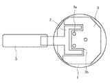
図1は、本発明の一実施例に係る基板搬送装置の基板搬入ステーションを示す平面図である。図1のように、本実施例に係わる基板搬送装置は、ウエハ1の保持部としてフィンガー2と、上下および水平に駆動させるハンドアーム5からなる搬送機構を持つ。温調プレート3には、フィンガー2の形状のきり欠き部3bが形成されており、フィンガー2を避ける形状となっているが、ウエハ1の大きさとほぼ一致する外形形状になっている。
【0015】
図2は本実施例に係る基板搬送装置の基板搬入ステーションの側面図を示す。温調プレート3には微小突起3aを設けてあり、この微少突起3aを介してウエハ1と接触している。温調プレート3とウエハ1の間の上下方向に、微少突起3aによって作られる空間、微少間隙30が形成される。
【0016】
図3は本実施例に係る基板搬送装置の基板搬入ステーションに外部からウエハ1を受け渡しするコータデベロッパー(以下C/Dと略す)ハンドの平面図を示す。C/Dハンド31が温調プレート3に干渉しない位置関係になっている。図4は本実施例に係る基板搬送装置の基板搬入ステーションに外部からウエハ1を受け渡しするC/Dハンドの側面図を示す。
【0017】
図5は本実施例に係る露光装置14の全体を示す平面図で、露光装置14の外側に張り出した基板搬入ステーション11と、ウエハ1を露光ステージ13ヘ運ぶ基板搬送装置12を示す。
【0018】
露光装置14内の基板搬送装置12の一連の動作を説明すると、まず装置14外部のC/Dハンド31から基板搬入ステーション11へウエハ1が受け渡され、この基板搬入ステーション11上にウエハ1は暫く放置される。露光ステージ13はウエハの露光を終了すると次のウエハを要求するので、基板搬送装置12が基板搬入ステーション11へウエハ1を受け取りに来る。その後ウエハ1は露光ステージ13に送られ、露光を開始する。
【0019】
次に基板搬入ステーション11でのウエハ1の温度調整を説明する。基板搬入ステーション11の温調プレート3に装置14外部からC/Dハンド31がウエハ1を受け渡しする。ウエハ1を温調プレート3上に載置し、ウエハ1と温調プレート3を接触させることによりウエハ1の温度調整を行なう。温調プレート3にはフィンガー2の形状の切り欠き部3bが形成されており、ウエハ1の温度調整が終了したら、温調プレート3上のウエハ1をフィンガー2を上下駆動させることによりフィンガー2上にウエハ1を取り上げ、ハンドアーム5でウエハ1を水平に移動させ、露光ステージ13ヘ搬送する。
【0020】
ウエハ1の温度調整方法は、基板搬入ステーションで温調プレート3に微少突起3aを設け、この微少突起3aによって作られる温調プレート3とウエハ1の間の空間である微少間隙30を介して、ウエハ1と温調プレート3との間で熱交換することにより行なうことができる。この微少間隙30は0.1〜0.2mm位にしておけば、熱交換は物体を直接接触させているのとほぼ同等の効果が得られる。このような非接触温度調整手段を用いれば温調プレート3とウエハ1を接触させる従来方式に比べ、ウエハの裏面のコンタミナントのパーティクルを減らすことができる。
【0021】
上記のような構成の基板搬送装置12を用いてウエハ1の搬送を行なえば、処理速度の違いにより、基板搬入ステーション11上でウエハ1が待機状態になっている間にウエハ1の温度調整を行なうことができるので、一連のシーケンス上無駄なくウエハ1の温度調整ができ、装置全体の処理速度を落とすことなくウエハ1の温度調整を行なうことができる。
【0022】
【発明の効果】
以上説明したように、本発明の基板搬送装置によれば、外部の搬送装置等から基板を受け取る基板搬入部材に基板温度の調整機能を設けることにより、基板の受け渡し途中の待機時間を利用して基板の温度調製を行なうことができ、装置全体の反応速度を落とすことがない。
【0023】
また、本発明の露光装置によれば、ウエハを露光ステージに搬送する基板搬送装置の、外部から基板を受け取る基板搬入ステーションに基板温度調整機能を設けることにより、ウエハの受け渡し途中の待機時間を利用して基板の温度調整を行なうことができ、装置全体の処理速度を落とすことはない。またウエハの受け渡し回数を最小にして、コンタミナント付着を増やすことなくウエハの温度調整を行なうことができる。また、温度調整されたウエハを用いることにより、更に精度の高いウエハの露光を行なうことができる。
【図面の簡単な説明】
【図1】 本発明の一実施例に係る基盤搬送装置の平面図を示す。
【図2】 本発明の一実施例に係る基板搬送装置の側面図を示す。
【図3】 本発明の一実施例に係る基盤搬送装置の平面図を示す。
【図4】 本発明の一実施例に係る基板搬送装置の側面図を示す。
【図5】 本発明の一実施例に係る露光装置の全体図を示す。
【符号の説明】
1:ウエハ、2:フィンガー、3:温調プレート、3a:微少突起、3b:切り欠き部、5:ハンドアーム、11:基板搬入ステーション、12:基板搬送装置、13:露光ステージ、14:露光装置、30:微少間隙、31:C/Dハンド。
Claims (3)
- 基板搬送装置において、
基板温調プレートを有し、コータデベロッパーハンドによって搬送された基板の温度を前記基板温調プレートにより調整する基板搬入ステーションと、
フィンガーを有し、前記基板搬入ステーションで温度調整された前記基板を前記フィンガーにより取り上げ、露光ステージへ搬送するハンドアームと、を備え、
前記基板温調プレートは、前記フィンガーが前記基板温調プレートに対して干渉せずに上下駆動できるように切り欠き部が形成された内形をしているとともに、前記コータデベロッパーハンドが前記基板温調プレートに対して干渉せずに上下駆動できるような外形をしていることを特徴とする基板搬送装置。 - 前記基板温調プレートは、前記基板と前記基板温調プレートの間の間隙を介して熱交換するように、前記基板を前記基板温調プレート上に支持する3つの突起部を有することを特徴とする請求項1に記載の基板搬送装置。
- 基板を露光する露光装置において、
露光ステージと、
請求項1または2に記載の基板搬送装置と、を備えることを特徴とする露光装置。
Priority Applications (3)
| Application Number | Priority Date | Filing Date | Title |
|---|---|---|---|
| JP13412999A JP4343326B2 (ja) | 1999-05-14 | 1999-05-14 | 基板搬送装置および露光装置 |
| US09/570,061 US6309212B1 (en) | 1999-05-14 | 2000-05-12 | Substrate conveying system and device manufacturing method using the same |
| US09/977,702 US6607380B1 (en) | 1999-05-14 | 2001-10-16 | Substrate conveying system and device manufacturing method using the same |
Applications Claiming Priority (1)
| Application Number | Priority Date | Filing Date | Title |
|---|---|---|---|
| JP13412999A JP4343326B2 (ja) | 1999-05-14 | 1999-05-14 | 基板搬送装置および露光装置 |
Publications (3)
| Publication Number | Publication Date |
|---|---|
| JP2000323553A JP2000323553A (ja) | 2000-11-24 |
| JP2000323553A5 JP2000323553A5 (ja) | 2006-06-22 |
| JP4343326B2 true JP4343326B2 (ja) | 2009-10-14 |
Family
ID=15121153
Family Applications (1)
| Application Number | Title | Priority Date | Filing Date |
|---|---|---|---|
| JP13412999A Expired - Fee Related JP4343326B2 (ja) | 1999-05-14 | 1999-05-14 | 基板搬送装置および露光装置 |
Country Status (2)
| Country | Link |
|---|---|
| US (2) | US6309212B1 (ja) |
| JP (1) | JP4343326B2 (ja) |
Families Citing this family (7)
| Publication number | Priority date | Publication date | Assignee | Title |
|---|---|---|---|---|
| JP4244555B2 (ja) | 2002-02-25 | 2009-03-25 | 東京エレクトロン株式会社 | 被処理体の支持機構 |
| JP4670677B2 (ja) * | 2006-02-17 | 2011-04-13 | 東京エレクトロン株式会社 | 加熱装置、加熱方法、塗布装置及び記憶媒体 |
| US8200354B2 (en) * | 2006-04-21 | 2012-06-12 | The Boeing Company | Assembly task verification system and method |
| JP4885023B2 (ja) * | 2007-03-23 | 2012-02-29 | 東京エレクトロン株式会社 | ロードロック装置および基板の処理システム |
| US20090174873A1 (en) * | 2007-12-17 | 2009-07-09 | Nikon Corporation | Exposure apparatus, exposure method and device manufacturing method |
| JP2010182906A (ja) * | 2009-02-06 | 2010-08-19 | Tokyo Electron Ltd | 基板処理装置 |
| JP5511536B2 (ja) * | 2010-06-17 | 2014-06-04 | 株式会社日立国際電気 | 基板処理装置及び半導体装置の製造方法 |
Family Cites Families (14)
| Publication number | Priority date | Publication date | Assignee | Title |
|---|---|---|---|---|
| US4539695A (en) * | 1984-01-06 | 1985-09-03 | The Perkin-Elmer Corporation | X-Ray lithography system |
| JPS60169148A (ja) * | 1984-02-13 | 1985-09-02 | Dainippon Screen Mfg Co Ltd | 基板の搬送方法及びその装置 |
| US4853880A (en) | 1985-08-23 | 1989-08-01 | Canon Kabushiki Kaisha | Device for positioning a semi-conductor wafer |
| US4887904A (en) | 1985-08-23 | 1989-12-19 | Canon Kabushiki Kaisha | Device for positioning a semi-conductor wafer |
| US4984953A (en) | 1987-02-20 | 1991-01-15 | Canon Kabushiki Kaisha | Plate-like article conveying system |
| JPH0333058Y2 (ja) * | 1987-06-26 | 1991-07-12 | ||
| KR970003907B1 (ko) * | 1988-02-12 | 1997-03-22 | 도오교오 에레구토론 가부시끼 가이샤 | 기판처리 장치 및 기판처리 방법 |
| JP3028462B2 (ja) * | 1995-05-12 | 2000-04-04 | 東京エレクトロン株式会社 | 熱処理装置 |
| TW353777B (en) * | 1996-11-08 | 1999-03-01 | Tokyo Electron Ltd | Treatment device |
| JP3333135B2 (ja) * | 1998-06-25 | 2002-10-07 | 東京エレクトロン株式会社 | 熱処理装置及び熱処理方法 |
| US6087632A (en) * | 1999-01-11 | 2000-07-11 | Tokyo Electron Limited | Heat processing device with hot plate and associated reflector |
| JP3635214B2 (ja) * | 1999-07-05 | 2005-04-06 | 東京エレクトロン株式会社 | 基板処理装置 |
| KR100348938B1 (ko) * | 1999-12-06 | 2002-08-14 | 한국디엔에스 주식회사 | 포토리소그라피 공정을 위한 반도체 제조장치 |
| US6402508B2 (en) * | 1999-12-09 | 2002-06-11 | Tokyo Electron Limited | Heat and cooling treatment apparatus and substrate processing system |
-
1999
- 1999-05-14 JP JP13412999A patent/JP4343326B2/ja not_active Expired - Fee Related
-
2000
- 2000-05-12 US US09/570,061 patent/US6309212B1/en not_active Expired - Lifetime
-
2001
- 2001-10-16 US US09/977,702 patent/US6607380B1/en not_active Expired - Lifetime
Also Published As
| Publication number | Publication date |
|---|---|
| JP2000323553A (ja) | 2000-11-24 |
| US6309212B1 (en) | 2001-10-30 |
| US6607380B1 (en) | 2003-08-19 |
Similar Documents
| Publication | Publication Date | Title |
|---|---|---|
| TWI244118B (en) | Exposure apparatus, substrate processing unit and lithographic system, and device manufacturing method | |
| KR101086174B1 (ko) | 도포·현상 장치 및 도포·현상 방법 | |
| KR101515247B1 (ko) | 기판 처리 장치 | |
| JPH08222616A (ja) | 基板処理装置 | |
| JP4279102B2 (ja) | 基板処理装置及び基板処理方法 | |
| JP4343326B2 (ja) | 基板搬送装置および露光装置 | |
| JP3880769B2 (ja) | 搬送装置の位置合わせ方法および基板処理装置 | |
| TW410415B (en) | Substrate carrying equipment and substrate processing equipment | |
| JP3936900B2 (ja) | 基板の処理システム | |
| CN110943005B (zh) | 基板处理装置以及基板处理方法 | |
| JP2006332558A (ja) | 基板の処理システム | |
| JP3504822B2 (ja) | 基板処理装置および基板処理用露光装置 | |
| JP3767811B2 (ja) | 基板処理装置、基板処理方法および塗布・現像装置 | |
| JPH0484410A (ja) | レジスト処理装置 | |
| JP2919123B2 (ja) | 板状体搬送装置 | |
| JP3912478B2 (ja) | 基板搬送装置 | |
| JP2926213B2 (ja) | 基板処理装置 | |
| JP2743274B2 (ja) | 基板処理装置および基板搬送装置 | |
| JP2926703B2 (ja) | 基板処理方法及び装置 | |
| JP3822752B2 (ja) | 処理装置 | |
| JP2926592B2 (ja) | 基板処理装置 | |
| JPH11274283A (ja) | 搬送方法及び搬送装置 | |
| JP3246659B2 (ja) | レジスト処理装置及び液処理装置及び基板処理装置 | |
| JP2003318245A (ja) | 基板搬送機構及び基板搬送方法 | |
| JP2010192559A (ja) | 基板処理システム |
Legal Events
| Date | Code | Title | Description |
|---|---|---|---|
| A521 | Request for written amendment filed |
Free format text: JAPANESE INTERMEDIATE CODE: A523 Effective date: 20060502 |
|
| A621 | Written request for application examination |
Free format text: JAPANESE INTERMEDIATE CODE: A621 Effective date: 20060502 |
|
| A977 | Report on retrieval |
Free format text: JAPANESE INTERMEDIATE CODE: A971007 Effective date: 20080827 |
|
| A131 | Notification of reasons for refusal |
Free format text: JAPANESE INTERMEDIATE CODE: A131 Effective date: 20080903 |
|
| A521 | Request for written amendment filed |
Free format text: JAPANESE INTERMEDIATE CODE: A523 Effective date: 20081031 |
|
| RD02 | Notification of acceptance of power of attorney |
Free format text: JAPANESE INTERMEDIATE CODE: A7422 Effective date: 20081031 |
|
| RD01 | Notification of change of attorney |
Free format text: JAPANESE INTERMEDIATE CODE: A7421 Effective date: 20090406 |
|
| TRDD | Decision of grant or rejection written | ||
| A01 | Written decision to grant a patent or to grant a registration (utility model) |
Free format text: JAPANESE INTERMEDIATE CODE: A01 Effective date: 20090707 |
|
| A01 | Written decision to grant a patent or to grant a registration (utility model) |
Free format text: JAPANESE INTERMEDIATE CODE: A01 |
|
| A61 | First payment of annual fees (during grant procedure) |
Free format text: JAPANESE INTERMEDIATE CODE: A61 Effective date: 20090709 |
|
| FPAY | Renewal fee payment (event date is renewal date of database) |
Free format text: PAYMENT UNTIL: 20120717 Year of fee payment: 3 |
|
| R150 | Certificate of patent or registration of utility model |
Free format text: JAPANESE INTERMEDIATE CODE: R150 |
|
| LAPS | Cancellation because of no payment of annual fees |