JP4294745B2 - 光電変換装置の作製方法 - Google Patents
光電変換装置の作製方法 Download PDFInfo
- Publication number
- JP4294745B2 JP4294745B2 JP27950297A JP27950297A JP4294745B2 JP 4294745 B2 JP4294745 B2 JP 4294745B2 JP 27950297 A JP27950297 A JP 27950297A JP 27950297 A JP27950297 A JP 27950297A JP 4294745 B2 JP4294745 B2 JP 4294745B2
- Authority
- JP
- Japan
- Prior art keywords
- photoelectric conversion
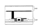
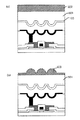
- curved portion
- lower electrode
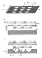
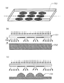
- forming
- resist
- Prior art date
- Legal status (The legal status is an assumption and is not a legal conclusion. Google has not performed a legal analysis and makes no representation as to the accuracy of the status listed.)
- Expired - Fee Related
Links
Images


Classifications
-
- H—ELECTRICITY
- H10—SEMICONDUCTOR DEVICES; ELECTRIC SOLID-STATE DEVICES NOT OTHERWISE PROVIDED FOR
- H10F—INORGANIC SEMICONDUCTOR DEVICES SENSITIVE TO INFRARED RADIATION, LIGHT, ELECTROMAGNETIC RADIATION OF SHORTER WAVELENGTH OR CORPUSCULAR RADIATION
- H10F39/00—Integrated devices, or assemblies of multiple devices, comprising at least one element covered by group H10F30/00, e.g. radiation detectors comprising photodiode arrays
- H10F39/10—Integrated devices
- H10F39/12—Image sensors
- H10F39/18—Complementary metal-oxide-semiconductor [CMOS] image sensors; Photodiode array image sensors
-
- H—ELECTRICITY
- H10—SEMICONDUCTOR DEVICES; ELECTRIC SOLID-STATE DEVICES NOT OTHERWISE PROVIDED FOR
- H10F—INORGANIC SEMICONDUCTOR DEVICES SENSITIVE TO INFRARED RADIATION, LIGHT, ELECTROMAGNETIC RADIATION OF SHORTER WAVELENGTH OR CORPUSCULAR RADIATION
- H10F39/00—Integrated devices, or assemblies of multiple devices, comprising at least one element covered by group H10F30/00, e.g. radiation detectors comprising photodiode arrays
- H10F39/011—Manufacture or treatment of image sensors covered by group H10F39/12
- H10F39/026—Wafer-level processing
-
- H—ELECTRICITY
- H10—SEMICONDUCTOR DEVICES; ELECTRIC SOLID-STATE DEVICES NOT OTHERWISE PROVIDED FOR
- H10F—INORGANIC SEMICONDUCTOR DEVICES SENSITIVE TO INFRARED RADIATION, LIGHT, ELECTROMAGNETIC RADIATION OF SHORTER WAVELENGTH OR CORPUSCULAR RADIATION
- H10F39/00—Integrated devices, or assemblies of multiple devices, comprising at least one element covered by group H10F30/00, e.g. radiation detectors comprising photodiode arrays
- H10F39/10—Integrated devices
- H10F39/12—Image sensors
- H10F39/191—Photoconductor image sensors
-
- H—ELECTRICITY
- H10—SEMICONDUCTOR DEVICES; ELECTRIC SOLID-STATE DEVICES NOT OTHERWISE PROVIDED FOR
- H10F—INORGANIC SEMICONDUCTOR DEVICES SENSITIVE TO INFRARED RADIATION, LIGHT, ELECTROMAGNETIC RADIATION OF SHORTER WAVELENGTH OR CORPUSCULAR RADIATION
- H10F39/00—Integrated devices, or assemblies of multiple devices, comprising at least one element covered by group H10F30/00, e.g. radiation detectors comprising photodiode arrays
- H10F39/80—Constructional details of image sensors
- H10F39/802—Geometry or disposition of elements in pixels, e.g. address-lines or gate electrodes
-
- H—ELECTRICITY
- H10—SEMICONDUCTOR DEVICES; ELECTRIC SOLID-STATE DEVICES NOT OTHERWISE PROVIDED FOR
- H10F—INORGANIC SEMICONDUCTOR DEVICES SENSITIVE TO INFRARED RADIATION, LIGHT, ELECTROMAGNETIC RADIATION OF SHORTER WAVELENGTH OR CORPUSCULAR RADIATION
- H10F39/00—Integrated devices, or assemblies of multiple devices, comprising at least one element covered by group H10F30/00, e.g. radiation detectors comprising photodiode arrays
- H10F39/80—Constructional details of image sensors
- H10F39/806—Optical elements or arrangements associated with the image sensors
- H10F39/8063—Microlenses
-
- H—ELECTRICITY
- H10—SEMICONDUCTOR DEVICES; ELECTRIC SOLID-STATE DEVICES NOT OTHERWISE PROVIDED FOR
- H10F—INORGANIC SEMICONDUCTOR DEVICES SENSITIVE TO INFRARED RADIATION, LIGHT, ELECTROMAGNETIC RADIATION OF SHORTER WAVELENGTH OR CORPUSCULAR RADIATION
- H10F77/00—Constructional details of devices covered by this subclass
- H10F77/40—Optical elements or arrangements
- H10F77/413—Optical elements or arrangements directly associated or integrated with the devices, e.g. back reflectors
-
- Y—GENERAL TAGGING OF NEW TECHNOLOGICAL DEVELOPMENTS; GENERAL TAGGING OF CROSS-SECTIONAL TECHNOLOGIES SPANNING OVER SEVERAL SECTIONS OF THE IPC; TECHNICAL SUBJECTS COVERED BY FORMER USPC CROSS-REFERENCE ART COLLECTIONS [XRACs] AND DIGESTS
- Y10—TECHNICAL SUBJECTS COVERED BY FORMER USPC
- Y10S—TECHNICAL SUBJECTS COVERED BY FORMER USPC CROSS-REFERENCE ART COLLECTIONS [XRACs] AND DIGESTS
- Y10S438/00—Semiconductor device manufacturing: process
- Y10S438/942—Masking
- Y10S438/948—Radiation resist
Landscapes
- Solid State Image Pick-Up Elements (AREA)
Priority Applications (4)
| Application Number | Priority Date | Filing Date | Title |
|---|---|---|---|
| JP27950297A JP4294745B2 (ja) | 1997-09-26 | 1997-09-26 | 光電変換装置の作製方法 |
| US09/160,619 US6288388B1 (en) | 1997-09-26 | 1998-09-24 | Photoelectric converter wherein the lower electrode has bends |
| US09/882,611 US6423569B2 (en) | 1997-09-26 | 2001-06-15 | Photoelectric converter and fabrication method thereof |
| US10/178,385 US6803261B2 (en) | 1997-09-26 | 2002-06-24 | Photoelectric converter and fabrication method thereof |
Applications Claiming Priority (1)
| Application Number | Priority Date | Filing Date | Title |
|---|---|---|---|
| JP27950297A JP4294745B2 (ja) | 1997-09-26 | 1997-09-26 | 光電変換装置の作製方法 |
Publications (3)
| Publication Number | Publication Date |
|---|---|
| JPH11103041A JPH11103041A (ja) | 1999-04-13 |
| JPH11103041A5 JPH11103041A5 (enExample) | 2005-06-16 |
| JP4294745B2 true JP4294745B2 (ja) | 2009-07-15 |
Family
ID=17611949
Family Applications (1)
| Application Number | Title | Priority Date | Filing Date |
|---|---|---|---|
| JP27950297A Expired - Fee Related JP4294745B2 (ja) | 1997-09-26 | 1997-09-26 | 光電変換装置の作製方法 |
Country Status (2)
| Country | Link |
|---|---|
| US (3) | US6288388B1 (enExample) |
| JP (1) | JP4294745B2 (enExample) |
Families Citing this family (34)
| Publication number | Priority date | Publication date | Assignee | Title |
|---|---|---|---|---|
| JP4271268B2 (ja) | 1997-09-20 | 2009-06-03 | 株式会社半導体エネルギー研究所 | イメージセンサおよびイメージセンサ一体型アクティブマトリクス型表示装置 |
| JP4294745B2 (ja) * | 1997-09-26 | 2009-07-15 | 株式会社半導体エネルギー研究所 | 光電変換装置の作製方法 |
| JP4044187B2 (ja) * | 1997-10-20 | 2008-02-06 | 株式会社半導体エネルギー研究所 | アクティブマトリクス型表示装置およびその作製方法 |
| JPH11326954A (ja) * | 1998-05-15 | 1999-11-26 | Semiconductor Energy Lab Co Ltd | 半導体装置 |
| JP2002057359A (ja) * | 2000-06-01 | 2002-02-22 | Sharp Corp | 積層型太陽電池 |
| US6828557B2 (en) * | 2000-06-08 | 2004-12-07 | Nikon Corporation | Radiation-detection devices |
| US6365926B1 (en) * | 2000-09-20 | 2002-04-02 | Eastman Kodak Company | CMOS active pixel with scavenging diode |
| US6891194B2 (en) | 2001-02-07 | 2005-05-10 | Sharp Kabushiki Kaisha | Active matrix substrate, electromagnetic detector, and liquid crystal display apparatus |
| US20030191693A1 (en) * | 2002-04-08 | 2003-10-09 | Itamar Aphek | System and method for conducting an advertising business |
| US7351605B2 (en) * | 2001-04-09 | 2008-04-01 | Semiconductor Energy Laboratory Co., Ltd. | Method of manufacturing a semiconductor device |
| JP4703883B2 (ja) | 2001-04-09 | 2011-06-15 | 株式会社半導体エネルギー研究所 | 半導体装置の作製方法 |
| JP2003218332A (ja) * | 2002-01-22 | 2003-07-31 | Sony Corp | 固体撮像素子 |
| US7067895B1 (en) * | 2003-01-10 | 2006-06-27 | Eastman Kodak Company | Color imager cell with transistors formed under the photodiodes |
| US6803250B1 (en) * | 2003-04-24 | 2004-10-12 | Taiwan Semiconductor Manufacturing Co., Ltd | Image sensor with complementary concave and convex lens layers and method for fabrication thereof |
| JP2006010859A (ja) * | 2004-06-23 | 2006-01-12 | Seiko Epson Corp | 電気光学装置及び電子機器、並びに電気光学装置の製造方法 |
| KR101133755B1 (ko) * | 2004-07-22 | 2012-04-09 | 삼성전자주식회사 | 표시 장치 및 표시 장치용 광원의 구동 장치 |
| US7029944B1 (en) * | 2004-09-30 | 2006-04-18 | Sharp Laboratories Of America, Inc. | Methods of forming a microlens array over a substrate employing a CMP stop |
| FR2893765A1 (fr) | 2005-11-21 | 2007-05-25 | St Microelectronics Sa | Circuit integre photosensible muni d'une couche reflective et procede de fabrication correspondant |
| US7923800B2 (en) * | 2006-12-27 | 2011-04-12 | Semiconductor Energy Laboratory Co., Ltd. | Semiconductor device and electronic device |
| KR100881276B1 (ko) * | 2007-09-07 | 2009-02-05 | 주식회사 동부하이텍 | 이미지 센서 및 그 제조방법 |
| US7875949B2 (en) * | 2008-02-28 | 2011-01-25 | Visera Technologies Company Limited | Image sensor device with submicron structure |
| US20090272422A1 (en) * | 2008-04-27 | 2009-11-05 | Delin Li | Solar Cell Design and Methods of Manufacture |
| US7759755B2 (en) | 2008-05-14 | 2010-07-20 | International Business Machines Corporation | Anti-reflection structures for CMOS image sensors |
| US8003425B2 (en) * | 2008-05-14 | 2011-08-23 | International Business Machines Corporation | Methods for forming anti-reflection structures for CMOS image sensors |
| KR101819757B1 (ko) | 2009-06-17 | 2018-01-17 | 더 리젠츠 오브 더 유니버시티 오브 미시간 | 평판 x-선 영상기에서의 포토다이오드 및 기타 센서 구조물, 및 박막 전자 회로에 기초하여 평판 x-선 영상기에서의 포토다이오드 및 기타 센서 구조물의 토폴로지적 균일성을 향상시키는 방법 |
| TWI475705B (zh) * | 2009-07-23 | 2015-03-01 | Kuo Ching Chiang | 具有聚光元件及高有效面積之太陽能電池及其製造方法 |
| US7986022B2 (en) * | 2009-11-19 | 2011-07-26 | International Business Machines Corporation | Semispherical integrated circuit structures |
| JP5873847B2 (ja) * | 2013-03-29 | 2016-03-01 | 富士フイルム株式会社 | 固体撮像素子および撮像装置 |
| US11791432B2 (en) * | 2013-05-22 | 2023-10-17 | W&Wsens Devices, Inc. | Microstructure enhanced absorption photosensitive devices |
| US9171873B2 (en) * | 2014-01-16 | 2015-10-27 | Taiwan Semiconductor Manufacturing Co., Ltd. | Light sensing integrated circuit and manufacturing method of sensing integrated circuit |
| US10038019B2 (en) | 2015-12-29 | 2018-07-31 | Industrial Technology Research Institute | Image sensor and manufacturing method thereof |
| US10181574B2 (en) | 2016-12-29 | 2019-01-15 | Lg Display Co., Ltd. | Organic light emitting device |
| US10418583B2 (en) | 2017-02-27 | 2019-09-17 | Lg Display Co., Ltd. | Organic light emitting device |
| TWI649865B (zh) * | 2017-09-06 | 2019-02-01 | 財團法人工業技術研究院 | 影像感測器及其製造方法 |
Family Cites Families (21)
| Publication number | Priority date | Publication date | Assignee | Title |
|---|---|---|---|---|
| JPS6045057A (ja) * | 1983-08-23 | 1985-03-11 | Toshiba Corp | 固体撮像装置の製造方法 |
| JPS61290408A (ja) * | 1985-06-18 | 1986-12-20 | Fuji Xerox Co Ltd | カラ−密着型イメ−ジセンサおよびその製造方法 |
| JP2890441B2 (ja) * | 1989-02-23 | 1999-05-17 | 工業技術院長 | 半導体装置 |
| US5172249A (en) * | 1989-05-31 | 1992-12-15 | Canon Kabushiki Kaisha | Photoelectric converting apparatus with improved switching to reduce sensor noises |
| TW198129B (enExample) * | 1990-06-21 | 1993-01-11 | Matsushita Electron Co Ltd | |
| US5076857A (en) * | 1990-08-27 | 1991-12-31 | Spire Corporation | Photovoltaic cell and process |
| JPH04268763A (ja) | 1991-02-23 | 1992-09-24 | Sony Corp | オンチップマイクロレンズの形成方法 |
| US5767559A (en) * | 1991-05-24 | 1998-06-16 | Fuji Xerox Co., Ltd. | Thin film type photoelectric conversion device |
| US5258077A (en) * | 1991-09-13 | 1993-11-02 | Solec International, Inc. | High efficiency silicon solar cells and method of fabrication |
| US5356488A (en) * | 1991-12-27 | 1994-10-18 | Rudolf Hezel | Solar cell and method for its manufacture |
| JP2974485B2 (ja) * | 1992-02-05 | 1999-11-10 | キヤノン株式会社 | 光起電力素子の製造法 |
| JPH05303116A (ja) * | 1992-02-28 | 1993-11-16 | Canon Inc | 半導体装置 |
| JPH06140650A (ja) * | 1992-09-14 | 1994-05-20 | Sanyo Electric Co Ltd | 透光性導電酸化膜の改質方法とこれを用いた光起電力装置の製造方法 |
| JP2795126B2 (ja) | 1993-04-16 | 1998-09-10 | 株式会社デンソー | 曲面加工方法及びその装置 |
| JP3792281B2 (ja) * | 1995-01-09 | 2006-07-05 | 株式会社半導体エネルギー研究所 | 太陽電池 |
| US5554229A (en) * | 1995-02-21 | 1996-09-10 | United Solar Systems Corporation | Light directing element for photovoltaic device and method of manufacture |
| JPH09101401A (ja) | 1995-10-05 | 1997-04-15 | Sony Corp | Lcd用マイクロレンズの形成方法 |
| US6294799B1 (en) * | 1995-11-27 | 2001-09-25 | Semiconductor Energy Laboratory Co., Ltd. | Semiconductor device and method of fabricating same |
| US6162658A (en) * | 1996-10-14 | 2000-12-19 | Unisearch Limited | Metallization of buried contact solar cells |
| US6096496A (en) * | 1997-06-19 | 2000-08-01 | Frankel; Robert D. | Supports incorporating vertical cavity emitting lasers and tracking apparatus for use in combinatorial synthesis |
| JP4294745B2 (ja) * | 1997-09-26 | 2009-07-15 | 株式会社半導体エネルギー研究所 | 光電変換装置の作製方法 |
-
1997
- 1997-09-26 JP JP27950297A patent/JP4294745B2/ja not_active Expired - Fee Related
-
1998
- 1998-09-24 US US09/160,619 patent/US6288388B1/en not_active Expired - Lifetime
-
2001
- 2001-06-15 US US09/882,611 patent/US6423569B2/en not_active Expired - Lifetime
-
2002
- 2002-06-24 US US10/178,385 patent/US6803261B2/en not_active Expired - Lifetime
Also Published As
| Publication number | Publication date |
|---|---|
| US6423569B2 (en) | 2002-07-23 |
| US6288388B1 (en) | 2001-09-11 |
| US20020158252A1 (en) | 2002-10-31 |
| US20010030279A1 (en) | 2001-10-18 |
| US6803261B2 (en) | 2004-10-12 |
| JPH11103041A (ja) | 1999-04-13 |
Similar Documents
| Publication | Publication Date | Title |
|---|---|---|
| JP4294745B2 (ja) | 光電変換装置の作製方法 | |
| KR0147401B1 (ko) | 고체촬상소자 및 그 제조방법 | |
| JP5538811B2 (ja) | 固体撮像素子 | |
| US7303931B2 (en) | Microfeature workpieces having microlenses and methods of forming microlenses on microfeature workpieces | |
| JP4310283B2 (ja) | 固体撮像装置およびこれを用いたカメラ | |
| US7897986B2 (en) | Microlens array and image sensing device using the same | |
| KR20060108378A (ko) | 3차원 구조를 갖는 이미지 센서의 분리형 단위화소 및 그제조방법 | |
| JP3178629B2 (ja) | 固体撮像装置およびその製造方法 | |
| TW200812077A (en) | Microlens for image sensor | |
| US7646551B2 (en) | Microlenses with patterned holes to produce a desired focus location | |
| JP2008547064A (ja) | 傾きのあるマイクロレンズの製造方法 | |
| KR101294470B1 (ko) | 고체촬상소자 | |
| JP2006229217A (ja) | 組み込み式光学素子を有するイメージセンサ | |
| JP3992713B2 (ja) | Cmosイメージセンサー及びその製造方法 | |
| JP2006054469A (ja) | イメージセンサ | |
| TW201117363A (en) | Photodetector array having electron lens | |
| JP2007305683A (ja) | 固体撮像素子の製造方法および固体撮像素子 | |
| CN100583446C (zh) | 图像传感器及其制造方法 | |
| JPH1070258A (ja) | 固体撮像素子およびその製造方法 | |
| JP2001358320A (ja) | 固体撮像素子及びその製造方法、並びにオンチップレンズ金型の製造方法 | |
| JP2007194606A (ja) | 光電変換装置、その製造方法、撮像モジュール及び撮像システム | |
| CN222532121U (zh) | 影像感测装置 | |
| JP2007201266A (ja) | マイクロレンズ、その製造方法、これを用いた固体撮像素子およびその製造方法 | |
| JP2004200334A (ja) | 固体撮像装置 | |
| JP2009525609A (ja) | イメージセンサーの製造方法 |
Legal Events
| Date | Code | Title | Description |
|---|---|---|---|
| A521 | Request for written amendment filed |
Free format text: JAPANESE INTERMEDIATE CODE: A523 Effective date: 20040922 |
|
| A621 | Written request for application examination |
Free format text: JAPANESE INTERMEDIATE CODE: A621 Effective date: 20040922 |
|
| A977 | Report on retrieval |
Free format text: JAPANESE INTERMEDIATE CODE: A971007 Effective date: 20060418 |
|
| A131 | Notification of reasons for refusal |
Free format text: JAPANESE INTERMEDIATE CODE: A131 Effective date: 20080603 |
|
| A521 | Request for written amendment filed |
Free format text: JAPANESE INTERMEDIATE CODE: A523 Effective date: 20080730 |
|
| A131 | Notification of reasons for refusal |
Free format text: JAPANESE INTERMEDIATE CODE: A131 Effective date: 20080826 |
|
| A521 | Request for written amendment filed |
Free format text: JAPANESE INTERMEDIATE CODE: A523 Effective date: 20081021 |
|
| A131 | Notification of reasons for refusal |
Free format text: JAPANESE INTERMEDIATE CODE: A131 Effective date: 20090120 |
|
| A521 | Request for written amendment filed |
Free format text: JAPANESE INTERMEDIATE CODE: A523 Effective date: 20090311 |
|
| TRDD | Decision of grant or rejection written | ||
| A01 | Written decision to grant a patent or to grant a registration (utility model) |
Free format text: JAPANESE INTERMEDIATE CODE: A01 Effective date: 20090407 |
|
| A01 | Written decision to grant a patent or to grant a registration (utility model) |
Free format text: JAPANESE INTERMEDIATE CODE: A01 |
|
| A61 | First payment of annual fees (during grant procedure) |
Free format text: JAPANESE INTERMEDIATE CODE: A61 Effective date: 20090409 |
|
| FPAY | Renewal fee payment (event date is renewal date of database) |
Free format text: PAYMENT UNTIL: 20120417 Year of fee payment: 3 |
|
| R150 | Certificate of patent or registration of utility model |
Free format text: JAPANESE INTERMEDIATE CODE: R150 |
|
| FPAY | Renewal fee payment (event date is renewal date of database) |
Free format text: PAYMENT UNTIL: 20120417 Year of fee payment: 3 |
|
| FPAY | Renewal fee payment (event date is renewal date of database) |
Free format text: PAYMENT UNTIL: 20120417 Year of fee payment: 3 |
|
| FPAY | Renewal fee payment (event date is renewal date of database) |
Free format text: PAYMENT UNTIL: 20130417 Year of fee payment: 4 |
|
| FPAY | Renewal fee payment (event date is renewal date of database) |
Free format text: PAYMENT UNTIL: 20130417 Year of fee payment: 4 |
|
| FPAY | Renewal fee payment (event date is renewal date of database) |
Free format text: PAYMENT UNTIL: 20140417 Year of fee payment: 5 |
|
| R250 | Receipt of annual fees |
Free format text: JAPANESE INTERMEDIATE CODE: R250 |
|
| R250 | Receipt of annual fees |
Free format text: JAPANESE INTERMEDIATE CODE: R250 |
|
| R250 | Receipt of annual fees |
Free format text: JAPANESE INTERMEDIATE CODE: R250 |
|
| LAPS | Cancellation because of no payment of annual fees |