JP4163004B2 - 光取り出し手段を持つ電界発光素子 - Google Patents
光取り出し手段を持つ電界発光素子 Download PDFInfo
- Publication number
- JP4163004B2 JP4163004B2 JP2002586411A JP2002586411A JP4163004B2 JP 4163004 B2 JP4163004 B2 JP 4163004B2 JP 2002586411 A JP2002586411 A JP 2002586411A JP 2002586411 A JP2002586411 A JP 2002586411A JP 4163004 B2 JP4163004 B2 JP 4163004B2
- Authority
- JP
- Japan
- Prior art keywords
- layer
- mirror
- tiling
- photons
- generation layer
- Prior art date
- Legal status (The legal status is an assumption and is not a legal conclusion. Google has not performed a legal analysis and makes no representation as to the accuracy of the status listed.)
- Expired - Fee Related
Links
- 238000000605 extraction Methods 0.000 title claims description 22
- 238000006243 chemical reaction Methods 0.000 claims description 34
- 239000000463 material Substances 0.000 claims description 22
- 239000013079 quasicrystal Substances 0.000 claims description 21
- 239000000758 substrate Substances 0.000 claims description 19
- 229910001218 Gallium arsenide Inorganic materials 0.000 claims description 15
- 239000004065 semiconductor Substances 0.000 claims description 14
- 239000004038 photonic crystal Substances 0.000 claims description 11
- 238000009826 distribution Methods 0.000 claims description 7
- 229910000980 Aluminium gallium arsenide Inorganic materials 0.000 claims description 5
- 229910045601 alloy Inorganic materials 0.000 claims description 5
- 239000000956 alloy Substances 0.000 claims description 5
- IJGRMHOSHXDMSA-UHFFFAOYSA-N Atomic nitrogen Chemical compound N#N IJGRMHOSHXDMSA-UHFFFAOYSA-N 0.000 claims description 4
- 239000011368 organic material Substances 0.000 claims description 4
- 229910000530 Gallium indium arsenide Inorganic materials 0.000 claims description 3
- RQNWIZPPADIBDY-UHFFFAOYSA-N arsenic atom Chemical compound [As] RQNWIZPPADIBDY-UHFFFAOYSA-N 0.000 claims description 3
- APFVFJFRJDLVQX-UHFFFAOYSA-N indium atom Chemical compound [In] APFVFJFRJDLVQX-UHFFFAOYSA-N 0.000 claims description 3
- 229920000620 organic polymer Polymers 0.000 claims description 3
- 125000002524 organometallic group Chemical group 0.000 claims description 3
- 229910052710 silicon Inorganic materials 0.000 claims description 3
- 239000010703 silicon Substances 0.000 claims description 3
- 239000004593 Epoxy Substances 0.000 claims description 2
- OAICVXFJPJFONN-UHFFFAOYSA-N Phosphorus Chemical compound [P] OAICVXFJPJFONN-UHFFFAOYSA-N 0.000 claims description 2
- XUIMIQQOPSSXEZ-UHFFFAOYSA-N Silicon Chemical compound [Si] XUIMIQQOPSSXEZ-UHFFFAOYSA-N 0.000 claims description 2
- 229910052782 aluminium Inorganic materials 0.000 claims description 2
- XAGFODPZIPBFFR-UHFFFAOYSA-N aluminium Chemical compound [Al] XAGFODPZIPBFFR-UHFFFAOYSA-N 0.000 claims description 2
- 229910052785 arsenic Inorganic materials 0.000 claims description 2
- 230000004888 barrier function Effects 0.000 claims description 2
- 238000000295 emission spectrum Methods 0.000 claims description 2
- 230000001747 exhibiting effect Effects 0.000 claims description 2
- 229910052738 indium Inorganic materials 0.000 claims description 2
- 229910052757 nitrogen Inorganic materials 0.000 claims description 2
- 229910052698 phosphorus Inorganic materials 0.000 claims description 2
- 239000011574 phosphorus Substances 0.000 claims description 2
- GYHNNYVSQQEPJS-UHFFFAOYSA-N Gallium Chemical compound [Ga] GYHNNYVSQQEPJS-UHFFFAOYSA-N 0.000 claims 1
- 229940058905 antimony compound for treatment of leishmaniasis and trypanosomiasis Drugs 0.000 claims 1
- 150000001463 antimony compounds Chemical class 0.000 claims 1
- 229910003460 diamond Inorganic materials 0.000 claims 1
- 239000010432 diamond Substances 0.000 claims 1
- 229910052733 gallium Inorganic materials 0.000 claims 1
- 229940093920 gynecological arsenic compound Drugs 0.000 claims 1
- 239000010410 layer Substances 0.000 description 33
- JBRZTFJDHDCESZ-UHFFFAOYSA-N AsGa Chemical compound [As]#[Ga] JBRZTFJDHDCESZ-UHFFFAOYSA-N 0.000 description 10
- 239000013598 vector Substances 0.000 description 8
- 238000010586 diagram Methods 0.000 description 7
- 238000000034 method Methods 0.000 description 4
- 229910018072 Al 2 O 3 Inorganic materials 0.000 description 3
- 238000005530 etching Methods 0.000 description 3
- 229910052751 metal Inorganic materials 0.000 description 3
- 239000002184 metal Substances 0.000 description 3
- 230000003647 oxidation Effects 0.000 description 3
- 238000007254 oxidation reaction Methods 0.000 description 3
- 229920005989 resin Polymers 0.000 description 3
- 239000011347 resin Substances 0.000 description 3
- 239000000969 carrier Substances 0.000 description 2
- 238000010894 electron beam technology Methods 0.000 description 2
- 239000011148 porous material Substances 0.000 description 2
- 229910005540 GaP Inorganic materials 0.000 description 1
- 229910004140 HfO Inorganic materials 0.000 description 1
- 229910004298 SiO 2 Inorganic materials 0.000 description 1
- 229910010413 TiO 2 Inorganic materials 0.000 description 1
- 230000002411 adverse Effects 0.000 description 1
- AZDRQVAHHNSJOQ-UHFFFAOYSA-N alumane Chemical compound [AlH3] AZDRQVAHHNSJOQ-UHFFFAOYSA-N 0.000 description 1
- 229910052787 antimony Inorganic materials 0.000 description 1
- WATWJIUSRGPENY-UHFFFAOYSA-N antimony atom Chemical compound [Sb] WATWJIUSRGPENY-UHFFFAOYSA-N 0.000 description 1
- 238000003486 chemical etching Methods 0.000 description 1
- 150000001875 compounds Chemical class 0.000 description 1
- 239000004020 conductor Substances 0.000 description 1
- 238000004049 embossing Methods 0.000 description 1
- 238000000407 epitaxy Methods 0.000 description 1
- 239000003822 epoxy resin Substances 0.000 description 1
- 229910052732 germanium Inorganic materials 0.000 description 1
- GNPVGFCGXDBREM-UHFFFAOYSA-N germanium atom Chemical compound [Ge] GNPVGFCGXDBREM-UHFFFAOYSA-N 0.000 description 1
- 239000011521 glass Substances 0.000 description 1
- PCHJSUWPFVWCPO-UHFFFAOYSA-N gold Chemical compound [Au] PCHJSUWPFVWCPO-UHFFFAOYSA-N 0.000 description 1
- 239000010931 gold Substances 0.000 description 1
- 229910052737 gold Inorganic materials 0.000 description 1
- 238000005286 illumination Methods 0.000 description 1
- 238000011065 in-situ storage Methods 0.000 description 1
- 239000011229 interlayer Substances 0.000 description 1
- 238000005304 joining Methods 0.000 description 1
- 238000004519 manufacturing process Methods 0.000 description 1
- 239000007769 metal material Substances 0.000 description 1
- 238000004377 microelectronic Methods 0.000 description 1
- QJGQUHMNIGDVPM-UHFFFAOYSA-N nitrogen(.) Chemical compound [N] QJGQUHMNIGDVPM-UHFFFAOYSA-N 0.000 description 1
- 230000003287 optical effect Effects 0.000 description 1
- TWNQGVIAIRXVLR-UHFFFAOYSA-N oxo(oxoalumanyloxy)alumane Chemical compound O=[Al]O[Al]=O TWNQGVIAIRXVLR-UHFFFAOYSA-N 0.000 description 1
- 230000000737 periodic effect Effects 0.000 description 1
- 229920000647 polyepoxide Polymers 0.000 description 1
- 230000001902 propagating effect Effects 0.000 description 1
- 238000004080 punching Methods 0.000 description 1
- 238000002310 reflectometry Methods 0.000 description 1
- 229910052594 sapphire Inorganic materials 0.000 description 1
- 239000010980 sapphire Substances 0.000 description 1
- HBMJWWWQQXIZIP-UHFFFAOYSA-N silicon carbide Chemical compound [Si+]#[C-] HBMJWWWQQXIZIP-UHFFFAOYSA-N 0.000 description 1
- 229910010271 silicon carbide Inorganic materials 0.000 description 1
- RJAVVKVGAZUUIE-UHFFFAOYSA-N stibanylidynephosphane Chemical compound [Sb]#P RJAVVKVGAZUUIE-UHFFFAOYSA-N 0.000 description 1
- GWEVSGVZZGPLCZ-UHFFFAOYSA-N titanium dioxide Inorganic materials O=[Ti]=O GWEVSGVZZGPLCZ-UHFFFAOYSA-N 0.000 description 1
- 238000001429 visible spectrum Methods 0.000 description 1
Images


Classifications
-
- H—ELECTRICITY
- H01—ELECTRIC ELEMENTS
- H01L—SEMICONDUCTOR DEVICES NOT COVERED BY CLASS H10
- H01L33/00—Semiconductor devices with at least one potential-jump barrier or surface barrier specially adapted for light emission; Processes or apparatus specially adapted for the manufacture or treatment thereof or of parts thereof; Details thereof
- H01L33/02—Semiconductor devices with at least one potential-jump barrier or surface barrier specially adapted for light emission; Processes or apparatus specially adapted for the manufacture or treatment thereof or of parts thereof; Details thereof characterised by the semiconductor bodies
- H01L33/10—Semiconductor devices with at least one potential-jump barrier or surface barrier specially adapted for light emission; Processes or apparatus specially adapted for the manufacture or treatment thereof or of parts thereof; Details thereof characterised by the semiconductor bodies with a light reflecting structure, e.g. semiconductor Bragg reflector
-
- H—ELECTRICITY
- H01—ELECTRIC ELEMENTS
- H01L—SEMICONDUCTOR DEVICES NOT COVERED BY CLASS H10
- H01L33/00—Semiconductor devices with at least one potential-jump barrier or surface barrier specially adapted for light emission; Processes or apparatus specially adapted for the manufacture or treatment thereof or of parts thereof; Details thereof
- H01L33/02—Semiconductor devices with at least one potential-jump barrier or surface barrier specially adapted for light emission; Processes or apparatus specially adapted for the manufacture or treatment thereof or of parts thereof; Details thereof characterised by the semiconductor bodies
- H01L33/20—Semiconductor devices with at least one potential-jump barrier or surface barrier specially adapted for light emission; Processes or apparatus specially adapted for the manufacture or treatment thereof or of parts thereof; Details thereof characterised by the semiconductor bodies with a particular shape, e.g. curved or truncated substrate
- H01L33/24—Semiconductor devices with at least one potential-jump barrier or surface barrier specially adapted for light emission; Processes or apparatus specially adapted for the manufacture or treatment thereof or of parts thereof; Details thereof characterised by the semiconductor bodies with a particular shape, e.g. curved or truncated substrate of the light emitting region, e.g. non-planar junction
-
- H—ELECTRICITY
- H10—SEMICONDUCTOR DEVICES; ELECTRIC SOLID-STATE DEVICES NOT OTHERWISE PROVIDED FOR
- H10K—ORGANIC ELECTRIC SOLID-STATE DEVICES
- H10K50/00—Organic light-emitting devices
- H10K50/80—Constructional details
- H10K50/85—Arrangements for extracting light from the devices
-
- H—ELECTRICITY
- H01—ELECTRIC ELEMENTS
- H01L—SEMICONDUCTOR DEVICES NOT COVERED BY CLASS H10
- H01L2224/00—Indexing scheme for arrangements for connecting or disconnecting semiconductor or solid-state bodies and methods related thereto as covered by H01L24/00
- H01L2224/01—Means for bonding being attached to, or being formed on, the surface to be connected, e.g. chip-to-package, die-attach, "first-level" interconnects; Manufacturing methods related thereto
- H01L2224/42—Wire connectors; Manufacturing methods related thereto
- H01L2224/47—Structure, shape, material or disposition of the wire connectors after the connecting process
- H01L2224/48—Structure, shape, material or disposition of the wire connectors after the connecting process of an individual wire connector
- H01L2224/4805—Shape
- H01L2224/4809—Loop shape
- H01L2224/48091—Arched
-
- H—ELECTRICITY
- H01—ELECTRIC ELEMENTS
- H01L—SEMICONDUCTOR DEVICES NOT COVERED BY CLASS H10
- H01L2224/00—Indexing scheme for arrangements for connecting or disconnecting semiconductor or solid-state bodies and methods related thereto as covered by H01L24/00
- H01L2224/01—Means for bonding being attached to, or being formed on, the surface to be connected, e.g. chip-to-package, die-attach, "first-level" interconnects; Manufacturing methods related thereto
- H01L2224/42—Wire connectors; Manufacturing methods related thereto
- H01L2224/47—Structure, shape, material or disposition of the wire connectors after the connecting process
- H01L2224/48—Structure, shape, material or disposition of the wire connectors after the connecting process of an individual wire connector
- H01L2224/481—Disposition
- H01L2224/48151—Connecting between a semiconductor or solid-state body and an item not being a semiconductor or solid-state body, e.g. chip-to-substrate, chip-to-passive
- H01L2224/48221—Connecting between a semiconductor or solid-state body and an item not being a semiconductor or solid-state body, e.g. chip-to-substrate, chip-to-passive the body and the item being stacked
- H01L2224/48245—Connecting between a semiconductor or solid-state body and an item not being a semiconductor or solid-state body, e.g. chip-to-substrate, chip-to-passive the body and the item being stacked the item being metallic
- H01L2224/48247—Connecting between a semiconductor or solid-state body and an item not being a semiconductor or solid-state body, e.g. chip-to-substrate, chip-to-passive the body and the item being stacked the item being metallic connecting the wire to a bond pad of the item
-
- H—ELECTRICITY
- H01—ELECTRIC ELEMENTS
- H01L—SEMICONDUCTOR DEVICES NOT COVERED BY CLASS H10
- H01L2224/00—Indexing scheme for arrangements for connecting or disconnecting semiconductor or solid-state bodies and methods related thereto as covered by H01L24/00
- H01L2224/73—Means for bonding being of different types provided for in two or more of groups H01L2224/10, H01L2224/18, H01L2224/26, H01L2224/34, H01L2224/42, H01L2224/50, H01L2224/63, H01L2224/71
- H01L2224/732—Location after the connecting process
- H01L2224/73251—Location after the connecting process on different surfaces
- H01L2224/73265—Layer and wire connectors
-
- H—ELECTRICITY
- H01—ELECTRIC ELEMENTS
- H01L—SEMICONDUCTOR DEVICES NOT COVERED BY CLASS H10
- H01L2933/00—Details relating to devices covered by the group H01L33/00 but not provided for in its subgroups
- H01L2933/0083—Periodic patterns for optical field-shaping in or on the semiconductor body or semiconductor body package, e.g. photonic bandgap structures
-
- H—ELECTRICITY
- H01—ELECTRIC ELEMENTS
- H01L—SEMICONDUCTOR DEVICES NOT COVERED BY CLASS H10
- H01L33/00—Semiconductor devices with at least one potential-jump barrier or surface barrier specially adapted for light emission; Processes or apparatus specially adapted for the manufacture or treatment thereof or of parts thereof; Details thereof
- H01L33/02—Semiconductor devices with at least one potential-jump barrier or surface barrier specially adapted for light emission; Processes or apparatus specially adapted for the manufacture or treatment thereof or of parts thereof; Details thereof characterised by the semiconductor bodies
- H01L33/20—Semiconductor devices with at least one potential-jump barrier or surface barrier specially adapted for light emission; Processes or apparatus specially adapted for the manufacture or treatment thereof or of parts thereof; Details thereof characterised by the semiconductor bodies with a particular shape, e.g. curved or truncated substrate
Description
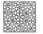
それは同等の割合の正方形と正三角形を示すか、または異なる頂点で第1および第2の角度の菱形を示し、その辺はほぼ近似した大きさでありうる;
それは選択された数の正三角形および正方形を含むパターンによる周期化もしくはスタンフリー(Stampfli)膨張、または異なる頂点で第1および第2の角度の菱形によって形成することができる;
それは選択された割合の正三角形と正方形のほぼランダムな分布、または異なる頂点で第1および第2の角度の菱形によって形成することができる。
下部ミラー5および上部ミラー14は、この非限定的な例では、ファブリ−ペロ型の共振電磁波マイクロキャビティを規定し、量子井戸において上部および下部ミラーにほぼ垂直な方向に生成したフォトンは外部へ透過し、他の残りはミラーの間、特に変換手段7の量子井戸を構成する層において導波モードの形態で閉じ込められる。
Kf=Ki+G。
Claims (23)
- 基板と、
前記基板に支持された下部ミラーと、
前記下部ミラー上に形成された電子生成層と、
前記電子生成層上に形成された変換層と、
前記変換層上に形成された正孔生成層と、
前記正孔生成層上に形成された上部ミラーと
を有する電界発光素子であって、前記変換層は電子−正孔対をフォトンに変換し、前記下部ミラーおよび上部ミラーは、電界発光素子の発光スペクトルの主波長であって導波モードに関連する選択された波長を示すフォトンの閉じ込めを確実にし、
さらに前記生成層および変換層の少なくとも一部に通じて前記生成層および変換層から導波モードにあるフォトンの少なくとも一部を取り出す光取り出し手段を有し、前記光取り出し手段は電子−正孔対の変換によってフォトンが生じる領域の周辺に形成された回折性の三次元フォトニック結晶または準結晶であり、前記フォトニック結晶または準結晶は導波モードにあるフォトンの波長に実質的に等しい寸法を有する
ことを特徴とする電界発光素子。 - 前記光取り出し手段は前記変換層および正孔生成層の少なくとも一部に形成されていることを特徴とする請求項1記載の素子。
- 前記光取り出し手段は前記電子生成層、変換層および正孔生成層の少なくとも一部に形成されていることを特徴とする請求項1記載の素子。
- 前記光取り出し手段は前記電子生成層、変換層、正孔生成層および上部ミラーの少なくとも一部に形成されていることを特徴とする請求項1記載の素子。
- 前記光取り出し手段は前記下部ミラー、電子生成層、変換層、正孔生成層および上部ミラーの少なくとも一部に形成されていることを特徴とする請求項1記載の素子。
- 前記準結晶は、実質的につながった多角形で、それらの辺の各々を唯一の隣と共有している凸面のタイリングであることを特徴とする請求項1に記載の素子。
- 前記タイリングは、実質的に等しい割合の正方形と正三角形、または頂点における角度が異なり実質的に等しいサイズの辺を持つ第1および第2の菱形からなることを特徴とする請求項6に記載の素子。
- 前記タイリングは、選択された数の正三角形および正方形を含むパターンの周期化、または頂点における角度が異なり実質的に等しいサイズの辺を持つ第1および第2の菱形からなることを特徴とする請求項6に記載の素子。
- 前記タイリングは、選択された数の正三角形および正方形を含むパターンのスタンフリー(Stampfli)膨張、または頂点における角度が異なり実質的に等しいサイズの辺を持つ第1および第2の菱形からなることを特徴とする請求項6に記載の素子。
- 前記タイリングは、選択された割合の正三角形および正方形の実質的にランダムな分布、または頂点における角度が異なり実質的に等しいサイズの辺を持つ第1および第2の菱形からなることを特徴とする請求項6に記載の素子。
- 前記タイリングは、前記電子生成層、変換層および正孔生成層を少なくとも部分的に囲んでいることを特徴とする請求項6ないし10のいずれか1項に記載の素子。
- 前記タイリングは湾曲し環状領域の少なくとも一部の上に広がっていることを特徴とする請求項6に記載の素子。
- 前記準結晶は回折要素の少なくとも1つが省略されているタイリングであることを特徴とする請求項6に記載の素子。
- 前記上部ミラーは半反射性タイプのものであり、正孔生成層と他の材料の層との間の界面によって形成されていることを特徴とする請求項1に記載の素子。
- 前記他の材料は、空気、エポキシおよび基板を形成する材料を含む群から選択されることを特徴とする請求項14に記載の素子。
- 前記下部ミラーは、基板上に設けられたブラッグミラータイプの反射ミラーであることを特徴とする請求項1に記載の素子。
- 前記電子生成層、変換層および正孔生成層の少なくとも一部は、半導体および有機電界発光材料を含む群より選択される材料からなることを特徴とする請求項1に記載の素子。
- 前記有機材料は、共役または非共役の有機ポリマー、および有機金属錯体を含む群より選択されることを特徴とする請求項17に記載の素子。
- 前記半導体は、シリコン、ガリウム、アルミニウム、インジウム、窒素、リン、ヒ素およびアンチモン系の化合物、ならびにこれらの合金を含む群より選択されることを特徴とする請求項17に記載の素子。
- i)GaAs基板と、前記下部ミラーを形成するGaAsとAlAsの交互層と、生成手段の一部を形成するnドープトGaAs層と、InGaAs中の量子井戸を囲む2つのAlGaAsバリアからなり、前記変換層を形成する活性層と、生成手段の一部および外部の空気と前記上部ミラーを形成するnドープトGaAsとをこの順に積層した積層体と、ii)pドープトGaAs層を正極性にさせる第1の電極コンタクト手段およびnドープトGaAs層を負極性にさせるのに適した第2の電極コンタクト手段とからなることを特徴とする請求項17に記載の素子。
- 前記上部ミラーおよび下部ミラーは、非対称の共振キャビティ、特にファブリ−ペロ型のものを規定することを特徴とする請求項1に記載の素子。
- 前記上部ミラーおよび下部ミラーは、変換層によって発せられるフォトンの波長を持つ反共振キャビティを規定することを特徴とする請求項1に記載の素子。
- 請求項1ないし22のいずれか1項の素子を有することを特徴とする電界発光ダイオード。
Applications Claiming Priority (2)
| Application Number | Priority Date | Filing Date | Title |
|---|---|---|---|
| FR0105652A FR2824228B1 (fr) | 2001-04-26 | 2001-04-26 | Dispositif electroluminescent a extracteur de lumiere |
| PCT/FR2002/001341 WO2002089218A2 (fr) | 2001-04-26 | 2002-04-18 | Dispositif electroluminescent a extracteur de lumiere |
Publications (3)
| Publication Number | Publication Date |
|---|---|
| JP2004521509A JP2004521509A (ja) | 2004-07-15 |
| JP2004521509A5 JP2004521509A5 (ja) | 2008-07-17 |
| JP4163004B2 true JP4163004B2 (ja) | 2008-10-08 |
Family
ID=8862739
Family Applications (1)
| Application Number | Title | Priority Date | Filing Date |
|---|---|---|---|
| JP2002586411A Expired - Fee Related JP4163004B2 (ja) | 2001-04-26 | 2002-04-18 | 光取り出し手段を持つ電界発光素子 |
Country Status (9)
| Country | Link |
|---|---|
| US (1) | US6987288B2 (ja) |
| EP (1) | EP1382074B1 (ja) |
| JP (1) | JP4163004B2 (ja) |
| AT (1) | ATE488027T1 (ja) |
| AU (1) | AU2002256752A1 (ja) |
| CA (1) | CA2444338C (ja) |
| DE (1) | DE60238245D1 (ja) |
| FR (1) | FR2824228B1 (ja) |
| WO (1) | WO2002089218A2 (ja) |
Families Citing this family (41)
| Publication number | Priority date | Publication date | Assignee | Title |
|---|---|---|---|---|
| JP3956918B2 (ja) | 2002-10-03 | 2007-08-08 | 日亜化学工業株式会社 | 発光ダイオード |
| JP2004172506A (ja) | 2002-11-22 | 2004-06-17 | Sony Corp | 半導体レーザ素子 |
| JP4610863B2 (ja) * | 2003-03-19 | 2011-01-12 | フィリップス ルミレッズ ライティング カンパニー リミテッド ライアビリティ カンパニー | フォトニック結晶構造を使用するled効率の改良 |
| US7078735B2 (en) | 2003-03-27 | 2006-07-18 | Sanyo Electric Co., Ltd. | Light-emitting device and illuminator |
| JP4263121B2 (ja) * | 2003-03-27 | 2009-05-13 | 三洋電機株式会社 | 発光素子および照明装置 |
| US7098589B2 (en) * | 2003-04-15 | 2006-08-29 | Luminus Devices, Inc. | Light emitting devices with high light collimation |
| US7083993B2 (en) * | 2003-04-15 | 2006-08-01 | Luminus Devices, Inc. | Methods of making multi-layer light emitting devices |
| US7166871B2 (en) * | 2003-04-15 | 2007-01-23 | Luminus Devices, Inc. | Light emitting systems |
| US6831302B2 (en) * | 2003-04-15 | 2004-12-14 | Luminus Devices, Inc. | Light emitting devices with improved extraction efficiency |
| US7262550B2 (en) * | 2003-04-15 | 2007-08-28 | Luminus Devices, Inc. | Light emitting diode utilizing a physical pattern |
| US20050173714A1 (en) * | 2004-02-06 | 2005-08-11 | Ho-Shang Lee | Lighting system with high and improved extraction efficiency |
| US7250635B2 (en) * | 2004-02-06 | 2007-07-31 | Dicon Fiberoptics, Inc. | Light emitting system with high extraction efficency |
| US7582910B2 (en) * | 2005-02-28 | 2009-09-01 | The Regents Of The University Of California | High efficiency light emitting diode (LED) with optimized photonic crystal extractor |
| US7442964B2 (en) | 2004-08-04 | 2008-10-28 | Philips Lumileds Lighting Company, Llc | Photonic crystal light emitting device with multiple lattices |
| JP2006059864A (ja) * | 2004-08-17 | 2006-03-02 | Yokohama National Univ | 発光素子 |
| US7509012B2 (en) * | 2004-09-22 | 2009-03-24 | Luxtaltek Corporation | Light emitting diode structures |
| JP4410123B2 (ja) | 2005-02-10 | 2010-02-03 | 株式会社東芝 | 有機elディスプレイ |
| JP2008311687A (ja) * | 2005-03-28 | 2008-12-25 | Stanley Electric Co Ltd | 自発光デバイス |
| KR100706796B1 (ko) * | 2005-08-19 | 2007-04-12 | 삼성전자주식회사 | 질화물계 탑에미트형 발광소자 및 그 제조 방법 |
| JP4843284B2 (ja) * | 2005-09-22 | 2011-12-21 | パナソニック電工株式会社 | 半導体発光素子およびその製造方法 |
| JP2007088273A (ja) * | 2005-09-22 | 2007-04-05 | Matsushita Electric Works Ltd | 半導体発光素子およびその製造方法 |
| US7717343B2 (en) * | 2006-01-12 | 2010-05-18 | Hand Held Products, Inc. | High-efficiency illumination in data collection devices |
| DE102006017573A1 (de) * | 2006-04-13 | 2007-10-18 | Osram Opto Semiconductors Gmbh | Optoelektronischer Halbleiterkörper und Verfahren zu dessen Herstellung |
| KR100736623B1 (ko) | 2006-05-08 | 2007-07-09 | 엘지전자 주식회사 | 수직형 발광 소자 및 그 제조방법 |
| EP2041802B1 (en) | 2006-06-23 | 2013-11-13 | LG Electronics Inc. | Light emitting diode having vertical topology and method of making the same |
| JP5168890B2 (ja) * | 2006-11-24 | 2013-03-27 | 日亜化学工業株式会社 | 半導体発光素子及び半導体発光素子の製造方法 |
| US8941566B2 (en) * | 2007-03-08 | 2015-01-27 | 3M Innovative Properties Company | Array of luminescent elements |
| JP5242975B2 (ja) * | 2007-09-03 | 2013-07-24 | 独立行政法人科学技術振興機構 | 回折格子型発光ダイオード |
| JP2009170508A (ja) * | 2008-01-11 | 2009-07-30 | Furukawa Electric Co Ltd:The | 面発光半導体レーザ及びその製造方法 |
| JP2011523212A (ja) * | 2008-06-05 | 2011-08-04 | スリーエム イノベイティブ プロパティズ カンパニー | 半導体波長変換器が接合された発光ダイオード |
| CN102124582B (zh) * | 2008-06-26 | 2013-11-06 | 3M创新有限公司 | 半导体光转换构造 |
| WO2009158159A2 (en) * | 2008-06-26 | 2009-12-30 | 3M Innovative Properties Company | Light converting construction |
| US20110101402A1 (en) * | 2008-06-26 | 2011-05-05 | Jun-Ying Zhang | Semiconductor light converting construction |
| WO2009158158A2 (en) * | 2008-06-26 | 2009-12-30 | 3M Innovative Properties Company | Method of fabricating light extractor |
| KR20100030472A (ko) * | 2008-09-10 | 2010-03-18 | 삼성전자주식회사 | 발광 소자 및 발광 장치의 제조 방법, 상기 방법을 이용하여 제조한 발광 소자 및 발광 장치 |
| KR20120038539A (ko) | 2009-07-30 | 2012-04-23 | 쓰리엠 이노베이티브 프로퍼티즈 컴파니 | 픽셀화된 led |
| JP2011187616A (ja) * | 2010-03-08 | 2011-09-22 | Toshiba Corp | 半導体発光素子およびその製造方法 |
| DE102014110069A1 (de) * | 2014-07-17 | 2016-01-21 | Osram Opto Semiconductors Gmbh | Verfahren zum Herstellen einer Strukturierungsmaske und einer Oberflächenstrukturierung |
| WO2017175201A2 (en) * | 2016-04-08 | 2017-10-12 | Novagan | Low etendue high brightness light emitting devices |
| FR3059788B1 (fr) | 2016-12-02 | 2019-01-25 | Commissariat A L'energie Atomique Et Aux Energies Alternatives | Dispositif optoelectronique a diode electroluminescente a extraction augmentee |
| FR3059787B1 (fr) * | 2016-12-02 | 2019-01-25 | Commissariat A L'energie Atomique Et Aux Energies Alternatives | Dispositif optoelectronique a diode electroluminescente a extraction augmentee |
Family Cites Families (3)
| Publication number | Priority date | Publication date | Assignee | Title |
|---|---|---|---|---|
| US5405710A (en) | 1993-11-22 | 1995-04-11 | At&T Corp. | Article comprising microcavity light sources |
| US5955749A (en) * | 1996-12-02 | 1999-09-21 | Massachusetts Institute Of Technology | Light emitting device utilizing a periodic dielectric structure |
| EP1371120B1 (en) * | 2001-03-09 | 2013-05-08 | Alight Photonics ApS | Mode control using transversal bandgap structure in vcsels |
-
2001
- 2001-04-26 FR FR0105652A patent/FR2824228B1/fr not_active Expired - Fee Related
-
2002
- 2002-04-18 AT AT02726265T patent/ATE488027T1/de not_active IP Right Cessation
- 2002-04-18 JP JP2002586411A patent/JP4163004B2/ja not_active Expired - Fee Related
- 2002-04-18 EP EP02726265A patent/EP1382074B1/fr not_active Expired - Lifetime
- 2002-04-18 DE DE60238245T patent/DE60238245D1/de not_active Expired - Lifetime
- 2002-04-18 CA CA2444338A patent/CA2444338C/fr not_active Expired - Fee Related
- 2002-04-18 AU AU2002256752A patent/AU2002256752A1/en not_active Abandoned
- 2002-04-18 WO PCT/FR2002/001341 patent/WO2002089218A2/fr active Application Filing
-
2003
- 2003-10-21 US US10/689,784 patent/US6987288B2/en not_active Expired - Lifetime
Also Published As
| Publication number | Publication date |
|---|---|
| CA2444338A1 (fr) | 2002-11-07 |
| DE60238245D1 (de) | 2010-12-23 |
| AU2002256752A1 (en) | 2002-11-11 |
| US20040141333A1 (en) | 2004-07-22 |
| US6987288B2 (en) | 2006-01-17 |
| JP2004521509A (ja) | 2004-07-15 |
| EP1382074B1 (fr) | 2010-11-10 |
| EP1382074A2 (fr) | 2004-01-21 |
| FR2824228B1 (fr) | 2003-08-01 |
| FR2824228A1 (fr) | 2002-10-31 |
| WO2002089218A3 (fr) | 2003-01-09 |
| WO2002089218A2 (fr) | 2002-11-07 |
| ATE488027T1 (de) | 2010-11-15 |
| CA2444338C (fr) | 2012-10-30 |
Similar Documents
| Publication | Publication Date | Title |
|---|---|---|
| JP4163004B2 (ja) | 光取り出し手段を持つ電界発光素子 | |
| JP2004521509A5 (ja) | ||
| US5966399A (en) | Vertical cavity surface emitting laser with integrated diffractive lens and method of fabrication | |
| US8492863B2 (en) | Optical modulator | |
| US10361250B2 (en) | Active optical device enabled by dielectric metamaterials | |
| US8410503B2 (en) | Light emitting devices | |
| JP4866108B2 (ja) | 単一光子発生デバイス、単一光子検出デバイス及び光量子ゲート | |
| JP2006157024A (ja) | 発光半導体素子 | |
| US10033158B1 (en) | Semiconductor laser, laser assembly and method of making a semiconductor laser | |
| KR102518449B1 (ko) | 유전체 dbr을 갖는 인듐 인화물 vcsel | |
| CN108879319B (zh) | 半导体元件 | |
| US20150010034A1 (en) | Short cavity surface emitting laser with double high contrast gratings with and without airgap | |
| CN109088308A (zh) | 具有高调制速度的垂直腔面发射激光器 | |
| KR20070075337A (ko) | 면발광형 반도체 레이저 | |
| TW202015254A (zh) | 具有光提取強化之利用內部色彩轉換之發光二極體 | |
| JP3219823B2 (ja) | 半導体発光素子 | |
| JP7242552B2 (ja) | 垂直共振器型面発光レーザ素子の製造方法 | |
| TW202032811A (zh) | 深紫外led裝置及其製造方法 | |
| TWI645637B (zh) | 面射型雷射裝置及其製造方法 | |
| CN111129953B (zh) | 一种激光器及其制造方法及激光器阵列 | |
| CN216288494U (zh) | 深紫外发光二极管 | |
| JP2023094519A (ja) | 光子源及び光子源を作製する方法 | |
| TW202335389A (zh) | 半導體雷射 |
Legal Events
| Date | Code | Title | Description |
|---|---|---|---|
| A621 | Written request for application examination |
Free format text: JAPANESE INTERMEDIATE CODE: A621 Effective date: 20050218 |
|
| A131 | Notification of reasons for refusal |
Free format text: JAPANESE INTERMEDIATE CODE: A131 Effective date: 20071225 |
|
| A601 | Written request for extension of time |
Free format text: JAPANESE INTERMEDIATE CODE: A601 Effective date: 20080325 |
|
| A602 | Written permission of extension of time |
Free format text: JAPANESE INTERMEDIATE CODE: A602 Effective date: 20080401 |
|
| A601 | Written request for extension of time |
Free format text: JAPANESE INTERMEDIATE CODE: A601 Effective date: 20080425 |
|
| A602 | Written permission of extension of time |
Free format text: JAPANESE INTERMEDIATE CODE: A602 Effective date: 20080507 |
|
| A524 | Written submission of copy of amendment under article 19 pct |
Free format text: JAPANESE INTERMEDIATE CODE: A524 Effective date: 20080526 |
|
| TRDD | Decision of grant or rejection written | ||
| A01 | Written decision to grant a patent or to grant a registration (utility model) |
Free format text: JAPANESE INTERMEDIATE CODE: A01 Effective date: 20080624 |
|
| A01 | Written decision to grant a patent or to grant a registration (utility model) |
Free format text: JAPANESE INTERMEDIATE CODE: A01 |
|
| A61 | First payment of annual fees (during grant procedure) |
Free format text: JAPANESE INTERMEDIATE CODE: A61 Effective date: 20080723 |
|
| FPAY | Renewal fee payment (event date is renewal date of database) |
Free format text: PAYMENT UNTIL: 20110801 Year of fee payment: 3 |
|
| R150 | Certificate of patent or registration of utility model |
Ref document number: 4163004 Country of ref document: JP Free format text: JAPANESE INTERMEDIATE CODE: R150 Free format text: JAPANESE INTERMEDIATE CODE: R150 |
|
| FPAY | Renewal fee payment (event date is renewal date of database) |
Free format text: PAYMENT UNTIL: 20120801 Year of fee payment: 4 |
|
| R250 | Receipt of annual fees |
Free format text: JAPANESE INTERMEDIATE CODE: R250 |
|
| FPAY | Renewal fee payment (event date is renewal date of database) |
Free format text: PAYMENT UNTIL: 20130801 Year of fee payment: 5 |
|
| R250 | Receipt of annual fees |
Free format text: JAPANESE INTERMEDIATE CODE: R250 |
|
| R250 | Receipt of annual fees |
Free format text: JAPANESE INTERMEDIATE CODE: R250 |
|
| R250 | Receipt of annual fees |
Free format text: JAPANESE INTERMEDIATE CODE: R250 |
|
| R250 | Receipt of annual fees |
Free format text: JAPANESE INTERMEDIATE CODE: R250 |
|
| R250 | Receipt of annual fees |
Free format text: JAPANESE INTERMEDIATE CODE: R250 |
|
| R250 | Receipt of annual fees |
Free format text: JAPANESE INTERMEDIATE CODE: R250 |
|
| R250 | Receipt of annual fees |
Free format text: JAPANESE INTERMEDIATE CODE: R250 |
|
| LAPS | Cancellation because of no payment of annual fees |