JP4113236B2 - 光機能回路 - Google Patents
光機能回路 Download PDFInfo
- Publication number
- JP4113236B2 JP4113236B2 JP2006523769A JP2006523769A JP4113236B2 JP 4113236 B2 JP4113236 B2 JP 4113236B2 JP 2006523769 A JP2006523769 A JP 2006523769A JP 2006523769 A JP2006523769 A JP 2006523769A JP 4113236 B2 JP4113236 B2 JP 4113236B2
- Authority
- JP
- Japan
- Prior art keywords
- light
- port
- optical
- output
- input
- Prior art date
- Legal status (The legal status is an assumption and is not a legal conclusion. Google has not performed a legal analysis and makes no representation as to the accuracy of the status listed.)
- Expired - Lifetime
Links
Images
Classifications
-
- G—PHYSICS
- G02—OPTICS
- G02B—OPTICAL ELEMENTS, SYSTEMS OR APPARATUS
- G02B6/00—Light guides; Structural details of arrangements comprising light guides and other optical elements, e.g. couplings
- G02B6/10—Light guides; Structural details of arrangements comprising light guides and other optical elements, e.g. couplings of the optical waveguide type
- G02B6/12—Light guides; Structural details of arrangements comprising light guides and other optical elements, e.g. couplings of the optical waveguide type of the integrated circuit kind
- G02B6/122—Basic optical elements, e.g. light-guiding paths
- G02B6/125—Bends, branchings or intersections
-
- G—PHYSICS
- G02—OPTICS
- G02B—OPTICAL ELEMENTS, SYSTEMS OR APPARATUS
- G02B6/00—Light guides; Structural details of arrangements comprising light guides and other optical elements, e.g. couplings
- G02B6/10—Light guides; Structural details of arrangements comprising light guides and other optical elements, e.g. couplings of the optical waveguide type
- G02B6/12—Light guides; Structural details of arrangements comprising light guides and other optical elements, e.g. couplings of the optical waveguide type of the integrated circuit kind
- G02B2006/12083—Constructional arrangements
- G02B2006/12119—Bend
-
- G—PHYSICS
- G02—OPTICS
- G02B—OPTICAL ELEMENTS, SYSTEMS OR APPARATUS
- G02B6/00—Light guides; Structural details of arrangements comprising light guides and other optical elements, e.g. couplings
- G02B6/10—Light guides; Structural details of arrangements comprising light guides and other optical elements, e.g. couplings of the optical waveguide type
- G02B6/12—Light guides; Structural details of arrangements comprising light guides and other optical elements, e.g. couplings of the optical waveguide type of the integrated circuit kind
- G02B2006/12083—Constructional arrangements
- G02B2006/1213—Constructional arrangements comprising photonic band-gap structures or photonic lattices
-
- G—PHYSICS
- G02—OPTICS
- G02B—OPTICAL ELEMENTS, SYSTEMS OR APPARATUS
- G02B6/00—Light guides; Structural details of arrangements comprising light guides and other optical elements, e.g. couplings
- G02B6/10—Light guides; Structural details of arrangements comprising light guides and other optical elements, e.g. couplings of the optical waveguide type
- G02B6/12—Light guides; Structural details of arrangements comprising light guides and other optical elements, e.g. couplings of the optical waveguide type of the integrated circuit kind
- G02B2006/12133—Functions
- G02B2006/12147—Coupler
Landscapes
- Physics & Mathematics (AREA)
- Engineering & Computer Science (AREA)
- Microelectronics & Electronic Packaging (AREA)
- General Physics & Mathematics (AREA)
- Optics & Photonics (AREA)
- Optical Integrated Circuits (AREA)
- Optical Couplings Of Light Guides (AREA)
Description
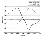
・φj(x):j番目の出射フィールド(複素ベクトル値関数であり、出射面において設定する強度分布および位相分布、ならびに、波長および偏波により規定される。)
なお、ψj(x)およびφj(x)は、回路中で強度増幅、波長変換、偏波変換が行われない限り、光強度の総和は同じ(あるいは無視できる程度の損失)であり、それらの波長も偏波も同じである。
{ψj(x)、φj(x)}は、入射面および出射面における、強度分布および位相分布ならびに波長および偏波により規定される。
与えられた入射フィールドおよび出射フィールドに対して屈折率分布を1つ与えたときに光のフィールドが決まるので、q番目の繰り返し演算で与えられる屈折率分布全体に対するフィールドを考える必要がある。そこで、(x,z)を不定変数として、屈折率分布全体をnq(x,z)と表しても良いが、場所(x,z)における屈折率の値nq(x,z)と区別するために、屈折率分布全体に対しては{nq}と表す。
・φj(z,x,{nq}):j番目の出射フィールドφj(x)を屈折率分布{nq}中をzまで逆伝搬させたときの、場所(x,z)におけるフィールドの値。
nq(z,x)=nq-1(z,x)−αΣjIm[φj(z,x,{nq-1})*・ψj(z,x,{nq-1})] ・・・(1)
ここで、右辺第2項中の記号「・」は、内積演算を意味し、Im[]は、[]内のフィールド内積演算結果の虚数成分を意味する。なお、記号「*」は複素共役である。係数αは、nq(z,x)の数分の1以下の値をさらにフィールドの組の数で割った値であり、正の小さな値である。Σjは、インデックスjについて和をとるという意味である。
Claims (3)
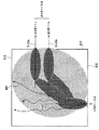
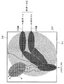
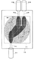
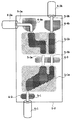
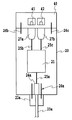
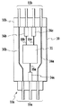
- 基板上に、クラッド層と、該クラッド層に埋設された前記クラッド層より高い屈折率を有するコア層とからなる光の導波領域が設けられた光機能回路において、
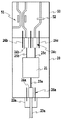
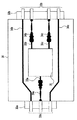
前記光の伝搬方向に垂直な断面において、前記光のフィールドの断面が与えられるべき回路上の場所をポートとし、任意の1個のポートから入射された入力光が、所定のポートから出力光として出射されるように、前記コア層に空間的な屈折率分布が形成された第1の波動伝達媒体を備え、
前記第1の波動伝達媒体の前記所定のポートから出射されない漏洩光が、他の回路要素と結合しないように、入力光として入力ポートから入射された前記漏洩光が、光路を変換されて、出力ポートから出力光として出射されるように、前記コア層に空間的な屈折率分布が形成された第2の波動伝達媒体を備え、
前記空間的な屈折率分布は、前記第1の波動伝達媒体の前記入力光が、前記任意の1個のポートから前記光の伝搬方向に沿って伝搬すると、前記入力光の入力フィールドが、前記出力光の出力フィールドに変換されて、前記所定のポートから出力される1つ以上の入出力フィールドの組の各々を伝搬するように、および前記第2の波動伝達媒体の前記入力光が、前記入力ポートから前記光の伝搬方向に沿って伝搬すると、前記入力光の入力フィールドが、前記出力光の出力フィールドに変換されて、前記出力ポートから出力される1つ以上の入出力フィールドの組の各々を伝搬するように、メッシュにより画定されるピクセルの各々のコアが有する屈折率によって決定され、
各々の前記ピクセルのコアの屈折率は、前記任意の1個のポートまたは前記入力ポートから前記所定のポートまたは前記出力ポートまでの光の伝搬方向の座標z、前記光の導波領域において前記光の伝搬方向に垂直な方向の座標xとしたときの断面Xの場所(z,x)において、前記入力フィールドの順伝搬のフィールドの位相と、前記出力フィールドの位相共役に逆伝搬させたフィールドの位相との間の位相差が所定の誤差以下となるように、各々の前記ピクセルのコアの屈折率を変数として繰り返し計算を行うことにより決定され、この計算は、(q−1)番目の計算によって得られた屈折率分布{nq -1}をもとに、前記入出力フィールドの組のj番目の入力フィールドψj(x)および出力フィールドφj(x)について、前記順伝搬フィールドψj(z,x,{nq -1})と前記逆伝搬のフィールドφj(z,x,{nq -1})としたとき、各場所(z,x)における屈折率nq(z,x)を、
nq(z,x)=nq -1(z,x)−αΣjIm[φj(z,x,{nq -1})*・ψj(z,x,{nq -1})]
として計算し、ここで、記号「*」は複素共役であり、記号「・」は内積演算であり、Im[]は[]内のフィールド内積演算結果の虚数成分であり、αは計算の収束を考慮した定数であり、Σjはjについて和を示し、かつ、
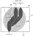
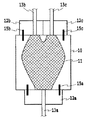
前記入力光のフィールドが、前記任意の1個のポートまたは前記入力ポートから前記所定のポートまたは前記出力ポートまでの伝搬方向に沿って、前記断面Xの屈折率分布により位相の変化を多段に受けることにより、前記第1および第2波動伝達媒体内で生じる伝搬波同士の多重散乱による干渉現象により光のフィールドの形状を変化させながら伝搬して、前記所定のポートまたは前記出力ポートから前記出力光の出力フィールドとして出射されることを特徴とする光機能回路。 - 前記第1の波動伝達媒体に画定された前記任意の1個のポートから入射された入力光のうち、前記第1の波動伝達媒体に画定された前記所定のポートから出射されない前記漏洩光が、前記第1の波動伝達媒体の前記所定のポートと異なる他のポートに結合されないように、前記任意の1個のポートの光軸と前記他のポートの光軸とは、互いに一致しないように配置されていることを特徴とする請求項1に記載の光機能回路。
- 前記任意の1個のポートから入射された入力光のビーム広がり角の半値θとすると、前記任意の1個のポートの光軸に対して、前記任意の1個のポートから角度θの2本の線に挟まれた領域の外側に、前記他のポートが配置されていることを特徴とする請求項2に記載の光機能回路。
Applications Claiming Priority (5)
| Application Number | Priority Date | Filing Date | Title |
|---|---|---|---|
| JP2004197313 | 2004-07-02 | ||
| JP2004197313 | 2004-07-02 | ||
| JP2004317092 | 2004-10-29 | ||
| JP2004317092 | 2004-10-29 | ||
| PCT/JP2005/012186 WO2006004031A1 (ja) | 2004-07-02 | 2005-07-01 | 光機能回路 |
Publications (2)
| Publication Number | Publication Date |
|---|---|
| JPWO2006004031A1 JPWO2006004031A1 (ja) | 2007-08-16 |
| JP4113236B2 true JP4113236B2 (ja) | 2008-07-09 |
Family
ID=35782835
Family Applications (1)
| Application Number | Title | Priority Date | Filing Date |
|---|---|---|---|
| JP2006523769A Expired - Lifetime JP4113236B2 (ja) | 2004-07-02 | 2005-07-01 | 光機能回路 |
Country Status (6)
| Country | Link |
|---|---|
| US (1) | US7580597B2 (ja) |
| EP (1) | EP1764635B1 (ja) |
| JP (1) | JP4113236B2 (ja) |
| KR (1) | KR100799659B1 (ja) |
| CA (1) | CA2552417C (ja) |
| WO (1) | WO2006004031A1 (ja) |
Families Citing this family (4)
| Publication number | Priority date | Publication date | Assignee | Title |
|---|---|---|---|---|
| JP4625420B2 (ja) * | 2006-04-04 | 2011-02-02 | 日本電信電話株式会社 | 光回路 |
| JP5071542B2 (ja) * | 2010-09-30 | 2012-11-14 | 住友大阪セメント株式会社 | 光導波路素子 |
| CN116802533A (zh) * | 2021-01-29 | 2023-09-22 | 京瓷株式会社 | 光路基板以及利用其的电子部件安装构造体 |
| US20240411157A1 (en) * | 2023-06-12 | 2024-12-12 | X Development Llc | Inverse designed photonic integrated circuit with improved signal to noise ratio |
Family Cites Families (17)
| Publication number | Priority date | Publication date | Assignee | Title |
|---|---|---|---|---|
| JPS60202553A (ja) * | 1984-03-27 | 1985-10-14 | Nec Corp | 導波路型光ヘツド |
| JP2773990B2 (ja) | 1991-04-15 | 1998-07-09 | 日本碍子株式会社 | 光導波路基板と光ファイバ整列用基板との結合体の製造方法 |
| JPH0511135A (ja) * | 1991-07-01 | 1993-01-19 | Furukawa Electric Co Ltd:The | 光フアイバと光導波路の接続方法 |
| JP2002031731A (ja) | 1993-08-09 | 2002-01-31 | Nippon Telegr & Teleph Corp <Ntt> | ハイブリッド光集積回路 |
| JPH08190028A (ja) | 1995-01-12 | 1996-07-23 | Hitachi Cable Ltd | N×mスプリッタ導波路素子及びその製造方法 |
| JP3151699B2 (ja) | 1995-05-18 | 2001-04-03 | 日本電信電話株式会社 | 光回路部品の作製方法 |
| JP3765140B2 (ja) * | 1996-12-19 | 2006-04-12 | 富士ゼロックス株式会社 | 光バスおよび信号処理装置 |
| JPH10332966A (ja) * | 1997-06-03 | 1998-12-18 | Nippon Telegr & Teleph Corp <Ntt> | 光デバイス |
| US6618535B1 (en) * | 2001-04-05 | 2003-09-09 | Nortel Networks Limited | Photonic bandgap device using coupled defects |
| US7373045B2 (en) | 2001-07-03 | 2008-05-13 | Brown University Research Foundation | Method and apparatus for processing optical signals with supergratings |
| US7116851B2 (en) * | 2001-10-09 | 2006-10-03 | Infinera Corporation | Optical signal receiver, an associated photonic integrated circuit (RxPIC), and method improving performance |
| JP2003344677A (ja) | 2002-05-29 | 2003-12-03 | Fujitsu Ltd | フォトニック結晶光導波路 |
| JP2004046021A (ja) * | 2002-07-15 | 2004-02-12 | Omron Corp | 光導波路装置、光合波分波装置及び光波長多重伝送装置 |
| JP2004163731A (ja) | 2002-11-14 | 2004-06-10 | Seiko Epson Corp | 光デバイスおよびその製造方法 |
| US7397977B2 (en) * | 2002-12-26 | 2008-07-08 | Nippon Telegraph And Telephone Corporation | Wave transmission medium and waveguide circuit |
| US7489846B2 (en) * | 2004-03-11 | 2009-02-10 | Agilent Technologies, Inc. | Photonic crystal sensors |
| JP2005352453A (ja) * | 2004-05-12 | 2005-12-22 | Nec Corp | 光ファイバ部品及び光導波路モジュール並びにこれらの製造方法 |
-
2005
- 2005-07-01 EP EP05755862.9A patent/EP1764635B1/en not_active Expired - Lifetime
- 2005-07-01 KR KR1020067012952A patent/KR100799659B1/ko not_active Expired - Lifetime
- 2005-07-01 WO PCT/JP2005/012186 patent/WO2006004031A1/ja not_active Ceased
- 2005-07-01 US US10/584,820 patent/US7580597B2/en not_active Expired - Lifetime
- 2005-07-01 JP JP2006523769A patent/JP4113236B2/ja not_active Expired - Lifetime
- 2005-07-01 CA CA002552417A patent/CA2552417C/en not_active Expired - Lifetime
Also Published As
| Publication number | Publication date |
|---|---|
| US7580597B2 (en) | 2009-08-25 |
| WO2006004031A1 (ja) | 2006-01-12 |
| EP1764635B1 (en) | 2018-04-25 |
| EP1764635A4 (en) | 2010-08-04 |
| CA2552417A1 (en) | 2006-01-12 |
| JPWO2006004031A1 (ja) | 2007-08-16 |
| EP1764635A1 (en) | 2007-03-21 |
| KR100799659B1 (ko) | 2008-01-30 |
| CA2552417C (en) | 2010-03-09 |
| US20080232736A1 (en) | 2008-09-25 |
| KR20060111624A (ko) | 2006-10-27 |
Similar Documents
| Publication | Publication Date | Title |
|---|---|---|
| CA2511944C (en) | Wave transmission medium and waveguide circuit | |
| WO2013046696A1 (ja) | 光合流分岐器、双方向光伝播器、及び光送受信システム | |
| JP3726062B2 (ja) | 光合分波器 | |
| US9151901B2 (en) | Wavelength-selective path-switching element | |
| Zhang et al. | Scalable and low crosstalk silicon mode exchanger for mode division multiplexing system enabled by inverse design | |
| JP4383815B2 (ja) | ホログラフィック波動伝達媒体の製造方法 | |
| JP4113236B2 (ja) | 光機能回路 | |
| US20020006249A1 (en) | Bragg grating assisted mmimi-coupler for tunable add-drop multiplexing | |
| JP2014182213A (ja) | 光素子 | |
| CN100399079C (zh) | 光学功能回路 | |
| JP2006030687A (ja) | 導波路型光合分波回路 | |
| JP3851314B2 (ja) | 光分岐回路、光送受信回路および光ネットワーク | |
| JP4069102B2 (ja) | 導波路型光合分波回路 | |
| JP4113161B2 (ja) | 光導波路型スイッチ | |
| JP4069101B2 (ja) | 導波路型光合分波回路 | |
| JP5118772B2 (ja) | 光インターコネクト | |
| JP2006126658A (ja) | 光導波路デバイス | |
| JP2003270460A (ja) | アレイ導波路格子型波長合分波器を含む集積光回路 | |
| KR20020008455A (ko) | 광분배기와 파장분할다중화모듈을 위한 저손실다중모드간섭계 | |
| JP4113162B2 (ja) | 光導波路およびその製造方法 | |
| Huang | Silicon photonic switching: from building block design to intelligent control | |
| JP2006039053A (ja) | 光機能回路 | |
| JP4126268B2 (ja) | アレイ導波路格子型光合分波回路 | |
| JP2006039052A (ja) | 光機能回路 | |
| JP2006058499A (ja) | 光導波路デバイス |
Legal Events
| Date | Code | Title | Description |
|---|---|---|---|
| A131 | Notification of reasons for refusal |
Free format text: JAPANESE INTERMEDIATE CODE: A131 Effective date: 20070622 |
|
| A521 | Request for written amendment filed |
Free format text: JAPANESE INTERMEDIATE CODE: A523 Effective date: 20070821 |
|
| A131 | Notification of reasons for refusal |
Free format text: JAPANESE INTERMEDIATE CODE: A131 Effective date: 20070918 |
|
| A521 | Request for written amendment filed |
Free format text: JAPANESE INTERMEDIATE CODE: A523 Effective date: 20071119 |
|
| A131 | Notification of reasons for refusal |
Free format text: JAPANESE INTERMEDIATE CODE: A131 Effective date: 20071228 |
|
| A521 | Request for written amendment filed |
Free format text: JAPANESE INTERMEDIATE CODE: A523 Effective date: 20080226 |
|
| TRDD | Decision of grant or rejection written | ||
| A01 | Written decision to grant a patent or to grant a registration (utility model) |
Free format text: JAPANESE INTERMEDIATE CODE: A01 Effective date: 20080404 |
|
| A61 | First payment of annual fees (during grant procedure) |
Free format text: JAPANESE INTERMEDIATE CODE: A61 Effective date: 20080410 |
|
| R151 | Written notification of patent or utility model registration |
Ref document number: 4113236 Country of ref document: JP Free format text: JAPANESE INTERMEDIATE CODE: R151 |
|
| FPAY | Renewal fee payment (event date is renewal date of database) |
Free format text: PAYMENT UNTIL: 20110418 Year of fee payment: 3 |
|
| FPAY | Renewal fee payment (event date is renewal date of database) |
Free format text: PAYMENT UNTIL: 20120418 Year of fee payment: 4 |
|
| FPAY | Renewal fee payment (event date is renewal date of database) |
Free format text: PAYMENT UNTIL: 20130418 Year of fee payment: 5 |
|
| FPAY | Renewal fee payment (event date is renewal date of database) |
Free format text: PAYMENT UNTIL: 20140418 Year of fee payment: 6 |
|
| S531 | Written request for registration of change of domicile |
Free format text: JAPANESE INTERMEDIATE CODE: R313531 |
|
| R350 | Written notification of registration of transfer |
Free format text: JAPANESE INTERMEDIATE CODE: R350 |
|
| EXPY | Cancellation because of completion of term |