JP4113236B2 - Optical functional circuit - Google Patents
Optical functional circuit Download PDFInfo
- Publication number
- JP4113236B2 JP4113236B2 JP2006523769A JP2006523769A JP4113236B2 JP 4113236 B2 JP4113236 B2 JP 4113236B2 JP 2006523769 A JP2006523769 A JP 2006523769A JP 2006523769 A JP2006523769 A JP 2006523769A JP 4113236 B2 JP4113236 B2 JP 4113236B2
- Authority
- JP
- Japan
- Prior art keywords
- light
- port
- optical
- output
- input
- Prior art date
- Legal status (The legal status is an assumption and is not a legal conclusion. Google has not performed a legal analysis and makes no representation as to the accuracy of the status listed.)
- Expired - Lifetime
Links
Images
Classifications
-
- G—PHYSICS
- G02—OPTICS
- G02B—OPTICAL ELEMENTS, SYSTEMS OR APPARATUS
- G02B6/00—Light guides; Structural details of arrangements comprising light guides and other optical elements, e.g. couplings
- G02B6/10—Light guides; Structural details of arrangements comprising light guides and other optical elements, e.g. couplings of the optical waveguide type
- G02B6/12—Light guides; Structural details of arrangements comprising light guides and other optical elements, e.g. couplings of the optical waveguide type of the integrated circuit kind
- G02B6/122—Basic optical elements, e.g. light-guiding paths
- G02B6/125—Bends, branchings or intersections
-
- G—PHYSICS
- G02—OPTICS
- G02B—OPTICAL ELEMENTS, SYSTEMS OR APPARATUS
- G02B6/00—Light guides; Structural details of arrangements comprising light guides and other optical elements, e.g. couplings
- G02B6/10—Light guides; Structural details of arrangements comprising light guides and other optical elements, e.g. couplings of the optical waveguide type
- G02B6/12—Light guides; Structural details of arrangements comprising light guides and other optical elements, e.g. couplings of the optical waveguide type of the integrated circuit kind
- G02B2006/12083—Constructional arrangements
- G02B2006/12119—Bend
-
- G—PHYSICS
- G02—OPTICS
- G02B—OPTICAL ELEMENTS, SYSTEMS OR APPARATUS
- G02B6/00—Light guides; Structural details of arrangements comprising light guides and other optical elements, e.g. couplings
- G02B6/10—Light guides; Structural details of arrangements comprising light guides and other optical elements, e.g. couplings of the optical waveguide type
- G02B6/12—Light guides; Structural details of arrangements comprising light guides and other optical elements, e.g. couplings of the optical waveguide type of the integrated circuit kind
- G02B2006/12083—Constructional arrangements
- G02B2006/1213—Constructional arrangements comprising photonic band-gap structures or photonic lattices
-
- G—PHYSICS
- G02—OPTICS
- G02B—OPTICAL ELEMENTS, SYSTEMS OR APPARATUS
- G02B6/00—Light guides; Structural details of arrangements comprising light guides and other optical elements, e.g. couplings
- G02B6/10—Light guides; Structural details of arrangements comprising light guides and other optical elements, e.g. couplings of the optical waveguide type
- G02B6/12—Light guides; Structural details of arrangements comprising light guides and other optical elements, e.g. couplings of the optical waveguide type of the integrated circuit kind
- G02B2006/12133—Functions
- G02B2006/12147—Coupler
Landscapes
- Physics & Mathematics (AREA)
- Engineering & Computer Science (AREA)
- Microelectronics & Electronic Packaging (AREA)
- General Physics & Mathematics (AREA)
- Optics & Photonics (AREA)
- Optical Integrated Circuits (AREA)
- Optical Couplings Of Light Guides (AREA)
Description
本発明は、光機能回路に関し、より詳細には、2次元的な屈折率分布に応じた多重散乱によりホログラフィックに波動を伝達させるホログラフィック波動伝達媒体を用いた光機能回路に関する。 The present invention relates to an optical functional circuit, and more particularly to an optical functional circuit using a holographic wave transmission medium that transmits waves holographically by multiple scattering according to a two-dimensional refractive index distribution.
光通信分野においては、光の分岐、干渉を容易に実現できる光回路として、光導波路構造を利用した集積光部品が開発されてきた。光の波動としての性質を利用した集積光部品は、光導波路長の調整により光干渉計の作製を容易にしたり、半導体分野における回路加工技術を適用することにより、光部品の集積化が容易になる。 In the optical communication field, integrated optical components using an optical waveguide structure have been developed as an optical circuit that can easily realize branching and interference of light. Integrated optical components that utilize the properties of light waves make it easy to manufacture optical interferometers by adjusting the length of the optical waveguide, or to easily integrate optical components by applying circuit processing technology in the semiconductor field. Become.
このような光導波路構造は、光導波路中を伝搬する光を屈折率の空間的分布を利用して空間的な光閉じ込めを実現する「光閉じ込め構造」である。光回路を構成するためには、光配線などを用いて、各構成要素を縦列的に接続することとなる。このため、光導波路回路の光路長は、光回路内で干渉現象などを生じさせるために求められる光路長よりも長くならざるを得ず、その結果、光回路そのものが極めて大型になってしまうという問題があった。 Such an optical waveguide structure is an “optical confinement structure” that realizes spatial light confinement of light propagating through the optical waveguide by utilizing a spatial distribution of refractive index. In order to configure an optical circuit, each component is connected in a cascade using an optical wiring or the like. For this reason, the optical path length of the optical waveguide circuit must be longer than the optical path length required for causing an interference phenomenon in the optical circuit, and as a result, the optical circuit itself becomes extremely large. There was a problem.
たとえば、典型的なアレイ導波路格子を例にとると、入力ポートから入力された複数の波長(λj)の光は、スラブ導波路を有するスターカプラにより分波・合波を繰り返し、分波された光が出力ポートから出力されるが、波長の千分の1程度の分解能で光を分波するために要する光路長は、導波路を伝搬する光の波長の数万倍となる。また、光回路の導波路パターンニングをはじめとして、偏光状態に依存する回路特性を補正するための波長板などを設けるための加工も施す必要がある。(例えば、非特許文献1参照)。 For example, taking a typical arrayed waveguide grating as an example, light of multiple wavelengths (λ j ) input from the input port is repeatedly demultiplexed and combined by a star coupler having a slab waveguide. The output light is output from the output port, but the optical path length required for demultiplexing the light with a resolution of about one thousandth of the wavelength is several tens of thousands of the wavelength of the light propagating through the waveguide. Moreover, it is necessary to perform processing for providing a wave plate for correcting circuit characteristics depending on the polarization state, including waveguide patterning of an optical circuit. (For example, refer nonpatent literature 1).
また、光回路の小型化のためには、光を導波路中に強く閉じ込める必要がある。従って、光導波路は、極めて大きな屈折率差を有する必要がある。例えば、従来のステップインデクッス型の光導波路では、比屈折率差が0.1%よりも大きな値となるように、屈折率の空間的分布を有するように光導波路を設計する。このような大きな屈折率差を利用して光閉じ込めを行うと、回路構成の自由度が制限されてしまう。特に、光導波路中での屈折率差を、局所的な紫外線照射、熱光学効果または電気光学効果などにより実現しようとしても、得られる屈折率の変化量は高々0.1%程度である。 In order to reduce the size of the optical circuit, it is necessary to strongly confine light in the waveguide. Therefore, the optical waveguide needs to have a very large refractive index difference. For example, in a conventional step index type optical waveguide, the optical waveguide is designed so as to have a spatial distribution of the refractive index so that the relative refractive index difference becomes a value larger than 0.1%. When optical confinement is performed using such a large refractive index difference, the degree of freedom in circuit configuration is limited. In particular, even if the refractive index difference in the optical waveguide is to be realized by local ultraviolet irradiation, the thermo-optic effect, or the electro-optic effect, the obtained refractive index variation is at most about 0.1%.
さらに、光の伝搬方向を変化させる場合に、光導波路の光路を小さい曲率で曲げると、伝搬する光が、光導波路から漏れ出してしまい、透過損失が大きくなるなど、回路特性が劣化する。従って、光の伝搬方向を変化させるには、光導波路の光路にそって徐々に向きを変化させざるを得ず、光回路長は必然的に極めて長いものとなり、その結果として光回路の小型化が困難になる。 Further, when the light propagation direction is changed, if the optical path of the optical waveguide is bent with a small curvature, the propagating light leaks from the optical waveguide, resulting in deterioration of circuit characteristics such as an increase in transmission loss. Therefore, in order to change the propagation direction of light, the direction must be gradually changed along the optical path of the optical waveguide, and the optical circuit length is inevitably extremely long. As a result, the optical circuit is downsized. Becomes difficult.
そこで、従来の光導波路回路、ホログラフィック回路を用いた光回路よりも小型で、緩やかな屈折率分布、すなわち小さな屈折率差でも充分に高効率の光信号制御を可能とする波動伝達媒体を用いることにより、高効率で小型の光回路を実現する。 Therefore, a wave transmission medium that is smaller than a conventional optical circuit using an optical waveguide circuit or a holographic circuit and has a gentle refractive index distribution, that is, sufficiently high-efficiency optical signal control even with a small refractive index difference is used. As a result, a highly efficient and compact optical circuit is realized.
しかしながら、波動伝達媒体は、仮想的なメッシュにより画定される仮想的なピクセルの各々が有する屈折率により、光信号を多重散乱させながら、入力ポートから出力ポートに伝播させる。従って、メッシュ状のピクセルを作製する際の作製誤差により、伝播光の漏洩が生じる。これにより、出力ポートに出力される伝搬光と、同一波長の漏洩した伝播光とが干渉を生じたり、波長が異なり干渉を生じない場合にもクロストークが発生する。 However, the wave transmission medium propagates the optical signal from the input port to the output port while performing multiple scattering by the refractive index of each virtual pixel defined by the virtual mesh. Therefore, leakage of propagating light occurs due to a manufacturing error in manufacturing a mesh pixel. As a result, the crosstalk occurs even when the propagated light output to the output port interferes with the leaked propagated light having the same wavelength or when the wavelength is different and no interference occurs.
また、波動伝達媒体は、干渉の効果を用いて伝播させるので、光路に大きな角度を持たせることができず、クロストークも大きい。干渉の効果は、入射する光の角度により異なるため、斜めに入射する成分の割合が高いことは、クロストークを劣化させる一因となる。特に、入出力ポート近傍の光のビーム径が小さい領域では、光の進行方向に対して斜めに入射する成分の割合が大きいので、クロストークを劣化させる。このようなクロストークの劣化により光回路の透過損失が大きくなるなど、回路特性が劣化するという問題があった。 In addition, since the wave transmission medium is propagated using the effect of interference, the optical path cannot have a large angle, and the crosstalk is large. Since the effect of interference varies depending on the angle of incident light, a high proportion of components incident obliquely contributes to the deterioration of crosstalk. In particular, in a region where the beam diameter of light in the vicinity of the input / output port is small, the ratio of components incident obliquely with respect to the traveling direction of light is large, so that crosstalk is degraded. There has been a problem that the circuit characteristics are deteriorated, for example, the transmission loss of the optical circuit is increased due to the deterioration of the crosstalk.
さらに、波動伝達媒体における入力ポート付近と出力ポート付近のメッシュ状のピクセルは、一種のレンズとして機能し、集光することができる。しかし、メッシュ状のピクセルのため、集光位置の判別が困難であり、他の光素子との接続が難しいという問題があった。 Furthermore, mesh-like pixels near the input port and the output port in the wave transmission medium function as a kind of lens and can be condensed. However, because of the mesh-like pixels, it is difficult to determine the condensing position and it is difficult to connect to other optical elements.
本発明の第1の目的は、ホログラフィック波動伝達媒体を適用し、透過損失、クロストークが小さいなど回路特性の良好な光機能回路を提供することにある。また、第2の目的は、ホログラフィック波動伝達媒体を適用した光導波路デバイスの接続を容易にして、透過損失、クロストークが小さい光機能回路を提供することにある。 A first object of the present invention is to provide an optical functional circuit having good circuit characteristics, such as transmission loss and small crosstalk, by applying a holographic wave transmission medium. A second object of the present invention is to provide an optical functional circuit that facilitates connection of an optical waveguide device to which a holographic wave transmission medium is applied, and has small transmission loss and crosstalk.
このような目的を達成するために、基板上に、クラッド層と、該クラッド層に埋設された前記クラッド層より高い屈折率を有するコア層とからなる光の導波領域が設けられた光機能回路は、光の伝搬方向に垂直な断面において、光のフィールドの断面が与えられるべき回路上の場所をポートとし、任意の1個のポートから入射された入力光が、所定のポートから出力光として出射されるように、前記コア層に空間的な屈折率分布が形成された第1の波動伝達媒体を備え、前記第1の波動伝達媒体の前記所定のポートから出射されない漏洩光が、他の回路要素と結合しないように、入力光として入力ポートから入射された前記漏洩光が、光路を変換されて、出力ポートから出力光として出射されるように、前記コア層に空間的な屈折率分布が形成された第2の波動伝達媒体をさらに備えた。 In order to achieve such an object, an optical function in which a light guide region comprising a clad layer and a core layer having a higher refractive index than the clad layer embedded in the clad layer is provided on a substrate. In the circuit, a section on the circuit where a section of the light field should be given in a section perpendicular to the light propagation direction is a port, and input light incident from any one port is output light from a predetermined port. as is emitted as comprising a first wave propagation medium spatial refractive index distribution is formed on the core layer, wherein the first leakage light that is not emitted from the predetermined port of the wave transmission medium, other so as not to bind to the circuit elements, the leakage light that entered from the input port as the input light is converted to the optical path, as is emitted as output light from the output port, the spatial refractive index to the core layer Distribution is shape Further comprising a second wave transmission medium is.
また、波動伝達媒体を含む光機能回路にあっては、第1の波動伝達媒体に画定された任意の1個のポートから入射された入力光のうち、第1の波動伝達媒体に画定された所定のポートから出射されない漏洩光が、第1の波動伝達媒体の所定のポートと異なるポートに結合されないように、任意の1個のポートの光軸と他のポートの光軸とは、互いに一致しないように配置されている。 Further, in the optical functional circuit including the wave transmission medium, the input light incident from one arbitrary port defined in the first wave transmission medium is defined in the first wave transmission medium. leakage light that is not emitted from a predetermined port, so as not to be bonded to a predetermined port different from the port of the first wave transmission medium, the optical axis and the optical axis of the other port of any one port, coincide with each other Arranged not to.
以下、図面を参照しながら本発明の実施形態について詳細に説明する。本実施形態の光機能回路は、複数の散乱点により画定されるホログラフィック波動伝達媒体であり、2次元的な屈折率分布に応じた多重散乱によりホログラフィックに波動を伝達させる。 Hereinafter, embodiments of the present invention will be described in detail with reference to the drawings. The optical functional circuit according to the present embodiment is a holographic wave transmission medium defined by a plurality of scattering points, and transmits waves holographically by multiple scattering according to a two-dimensional refractive index distribution.
最初に、本願発明に用いる波動伝達媒体の基本的概念について説明する。ここでは、光回路へ適用することから、波動伝達媒体中を伝搬する「波動」は「光」である。なお、波動伝達媒体にかかる理論は、一般の波動方程式に基づいて、媒質の特性を指定するものであり、一般の波動においても原理的に成り立ち得るものである。波動伝達媒体は、コヒーレントな光のパターンを入力して所望の光のパターンを出力させるために、波動伝達媒体中を伝搬する順伝搬光と逆伝搬光の位相差が、波動伝達媒体中の何れの場所においても小さくなるように屈折率分布が決定される。屈折率分布に応じた局所的なレベルのホログラフィック制御を多重に繰り返すことにより、所望の光のパターンが出力される。 First, the basic concept of the wave transmission medium used in the present invention will be described. Here, since it is applied to an optical circuit, the “wave” propagating in the wave transmission medium is “light”. The theory relating to the wave transmission medium specifies the characteristics of the medium based on a general wave equation, and can also hold in principle in general waves. In order to input a coherent light pattern and output a desired light pattern, the wave transmission medium has a phase difference between forward propagation light and back propagation light propagating in the wave transmission medium. The refractive index distribution is determined so as to be small even at the location. A desired light pattern is output by repeatedly repeating holographic control at a local level according to the refractive index distribution.
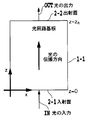
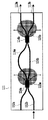
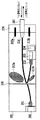
図1A〜Cを参照して、本実施形態にかかる波動伝達媒体の基本構造を説明する。図1Aに示したように、光回路基板1の中に、波動伝達媒体により構成される光回路の設計領域1−1が存在する。光回路の一方の端面は、入力光INが入射する入射面2−1である。入力光INは、波動伝達媒体で構成された空間的な屈折率分布を有する光回路中を多重散乱しながら伝搬し、他方の端面である出射面2−2から出力光OUTとして出力される。図1A中の座標zは、光の伝搬方向の座標(z=0が入射面、z=zeが出射面)であり、座標xは、光の伝搬方向に対する横方向の座標である。なお、本実施形態では、波動伝達媒体は、誘電体からなるものと仮定し、空間的な屈折率分布は、波動伝達媒体を構成している誘電体の局所的な屈折率を後述する理論に基づいて設定することにより実現される。
The basic structure of the wave transmission medium according to the present embodiment will be described with reference to FIGS. As shown in FIG. 1A, an optical circuit design area 1-1 composed of a wave transmission medium exists in the
入力光INが形成している「場」(入力フィールド)は、光回路を構成する波動伝達媒体の屈折率の空間的分布に応じて変調され、出力光OUTの形成する「場」(出力フィールド)に変換される。換言すれば、本発明の波動伝達媒体は、その空間的な屈折率分布に応じて入力フィールドと出力フィールドとを相関づけるための(電磁)フィールド変換手段である。なお、これら入力フィールドおよび出力フィールドに対して、光回路中での伝搬方向(図中z軸方向)に垂直な断面(図中x軸に沿う断面)における光のフィールドを、その場所(x,z)における(順)伝搬像(伝搬フィールドあるいは伝搬光)と呼ぶ(図1B参照)。 The “field” (input field) formed by the input light IN is modulated according to the spatial distribution of the refractive index of the wave transmission medium constituting the optical circuit, and the “field” (output field) formed by the output light OUT. ). In other words, the wave transmission medium of the present invention is (electromagnetic) field conversion means for correlating the input field and the output field according to the spatial refractive index distribution. For these input field and output field, the light field in the cross section (cross section along the x axis in the figure) perpendicular to the propagation direction (z axis direction in the figure) in the optical circuit is represented by its location (x, This is called a (forward) propagation image (propagation field or propagation light) in z) (see FIG. 1B).
ここで、「フィールド」とは、一般に電磁場(電磁界)または電磁場のベクトルポテンシャル場を意味している。本実施形態における電磁場の制御は、光回路中に設けられた空間的な屈折率分布、すなわち誘電率の分布を変えることに相当する。誘電率はテンソルとして与えられるが、通常は偏光状態間の遷移はそれほど大きくないので、電磁場の1成分のみを対象としてスカラー波近似しても良い近似となる。そこで、本明細書では電磁場を複素スカラー波として扱う。なお、光の「状態」には、エネルギ状態(波長)と偏光状態とがあるため、「フィールド」を光の状態を表現するものとして用いる場合には、光の波長と偏光状態をも包含し得ることとなる。 Here, “field” generally means an electromagnetic field (electromagnetic field) or a vector potential field of an electromagnetic field. The control of the electromagnetic field in this embodiment corresponds to changing the spatial refractive index distribution provided in the optical circuit, that is, the dielectric constant distribution. Although the dielectric constant is given as a tensor, since the transition between the polarization states is usually not so large, it is an approximation that may be a scalar wave approximation for only one component of the electromagnetic field. Therefore, in this specification, the electromagnetic field is treated as a complex scalar wave. Since the “state” of light includes an energy state (wavelength) and a polarization state, when the “field” is used to express the state of light, the light wavelength and polarization state are also included. Will get.
また、通常、伝搬光の増幅や減衰を生じさせない光回路では、屈折率の空間的分布を決めると、焦点以外の入力光INの像(入力フィールド)は、出力光OUTの像(出力フィールド)に対して一意的に定まる。このような、出射面2−2側から入射面2−1側へと向かう光のフィールドを、逆伝搬像(逆伝搬フィールドあるいは逆伝搬光)と呼ぶ(図1C参照)。このような逆伝搬像は、光回路中の場所ごとに定義することができる。すなわち、光回路中での任意の場所における光のフィールドを考えたとき、その場所を仮想的な「入力光」の出射点として考えれば、上記と同様に出力光OUTの像に対して、その場所での逆伝搬像を考えることができる。このように、光回路中の各場所ごとに逆伝搬像が定義できる。 In general, in an optical circuit that does not cause amplification or attenuation of propagating light, when the spatial distribution of the refractive index is determined, the image of the input light IN other than the focus (input field) is the image of the output light OUT (output field). Is uniquely determined. Such a field of light traveling from the exit surface 2-2 side to the entrance surface 2-1 side is referred to as a back propagation image (a back propagation field or a back propagation light) (see FIG. 1C). Such a back propagation image can be defined for each place in the optical circuit. That is, when considering a light field at an arbitrary place in an optical circuit, if the place is considered as a virtual “input light” emission point, A back propagation image at a place can be considered. In this way, a back propagation image can be defined for each location in the optical circuit.
特に、単一の光回路において、出射フィールドが入射フィールドの伝搬フィールドとなっている場合には、光回路の任意の点で、伝搬フィールドと逆伝搬フィールドとは一致する。なお、フィールドは、一般的に、対象とする空間全体の上の関数であるが、「入射フィールド」または「出射フィールド」という場合は、入射面あるいは出射面におけるフィールドの断面を意味している。また、「フィールド分布」という場合でも、ある特定の断面に関して議論を行う場合には、その断面についてのフィールドの断面を意味している。 In particular, in a single optical circuit, when the outgoing field is a propagation field of the incident field, the propagation field and the reverse propagation field coincide with each other at any point of the optical circuit. The field is generally a function over the entire target space, but the term “incident field” or “exit field” means a cross section of the field on the entrance surface or exit surface. In addition, even in the case of “field distribution”, when a discussion is made regarding a specific cross section, it means a cross section of the field with respect to that cross section.
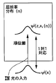
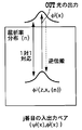
屈折率分布の決定方法を説明するためには記号を用いるほうが見通しがよいので、各量を表すために以下のような記号を用いることとする。なお、対象とされる光(フィールド)は、単一状態の光には限定されないので、複数の状態の光が重畳された光を対象とされ得るべく、個々の状態の光にインデックスjを充てて一般的に表記する。 In order to explain the method of determining the refractive index distribution, it is better to use symbols, so the following symbols are used to represent each quantity. Note that the target light (field) is not limited to light in a single state. Therefore, an index j is assigned to light in each state so that light in which a plurality of states are superimposed can be targeted. In general.
・ψj(x):j番目の入射フィールド(複素ベクトル値関数であり、入射面において設定する強度分布および位相の分布、ならびに、波長および偏波により規定される。)
・φj(x):j番目の出射フィールド(複素ベクトル値関数であり、出射面において設定する強度分布および位相分布、ならびに、波長および偏波により規定される。)
なお、ψj(x)およびφj(x)は、回路中で強度増幅、波長変換、偏波変換が行われない限り、光強度の総和は同じ(あるいは無視できる程度の損失)であり、それらの波長も偏波も同じである。
Ψ j (x): j-th incident field (complex vector value function, defined by intensity distribution and phase distribution set on the incident surface, and wavelength and polarization)
Φ j (x): j-th outgoing field (complex vector value function, defined by intensity distribution and phase distribution, wavelength and polarization set on the outgoing face)
Note that ψ j (x) and φ j (x) have the same total light intensity (or a negligible loss) unless intensity amplification, wavelength conversion, and polarization conversion are performed in the circuit. Their wavelength and polarization are the same.
・{ψj(x)、φj(x)}:入出力ペア(入出力のフィールドの組み。)
{ψj(x)、φj(x)}は、入射面および出射面における、強度分布および位相分布ならびに波長および偏波により規定される。
{Ψ j (x), φ j (x)}: Input / output pair (a set of input / output fields)
{Ψ j (x), φ j (x)} is defined by the intensity distribution and the phase distribution, the wavelength and the polarization at the entrance surface and the exit surface.
・{nq}:屈折率分布(光回路設計領域全体の値の組。)
与えられた入射フィールドおよび出射フィールドに対して屈折率分布を1つ与えたときに光のフィールドが決まるので、q番目の繰り返し演算で与えられる屈折率分布全体に対するフィールドを考える必要がある。そこで、(x,z)を不定変数として、屈折率分布全体をnq(x,z)と表しても良いが、場所(x,z)における屈折率の値nq(x,z)と区別するために、屈折率分布全体に対しては{nq}と表す。
{N q }: Refractive index distribution (a set of values for the entire optical circuit design area)
Since one field of light is determined when one refractive index distribution is given to a given incident field and outgoing field, it is necessary to consider a field for the entire refractive index distribution given by the qth iterative operation. Therefore, the entire refractive index distribution may be expressed as n q (x, z) with (x, z) as an indefinite variable, but the refractive index value n q (x, z) at the location (x, z) For distinction, {n q } is used for the entire refractive index distribution.
・ncore:光導波路におけるコア部分のような、周囲の屈折率に対して高い屈折率の値を示す記号。 N core : A symbol indicating a high refractive index value with respect to the surrounding refractive index, such as a core portion in an optical waveguide.
・nclad:光導波路におけるクラッド部分のような、ncoreに対して低い屈折率の値を示す記号。 N clad : a symbol indicating a low refractive index value with respect to n core , such as a clad portion in an optical waveguide.
・ψj(z,x,{nq}):j番目の入射フィールドψj(x)を屈折率分布{nq}中をzまで伝搬させたときの、場所(x,z)におけるフィールドの値。
・φj(z,x,{nq}):j番目の出射フィールドφj(x)を屈折率分布{nq}中をzまで逆伝搬させたときの、場所(x,z)におけるフィールドの値。
Ψ j (z, x, {n q }): field at location (x, z) when the jth incident field ψ j (x) is propagated through the refractive index profile {n q } to z The value of the.
Φ j (z, x, {n q }): at the location (x, z) when the j-th outgoing field φ j (x) is propagated back to z in the refractive index profile {n q } The field value.
本実施形態において、屈折率分布は、すべてのjについてψj(ze,x,{nq})=φj(x)、またはそれに近い状態となるように{nq}が与えられる。 In the present embodiment, the refractive index distribution, all j for ψ j (z e, x, {n q}) is given = φ j (x), or the so close state {n q}.
「入力ポート」および「出力ポート」とは、入射端面および出射端面におけるフィールドの集中した「領域」であり、例えば、その部分に光ファイバを接続することにより、光強度をファイバに伝搬できるような領域である。ここで、フィールドの強度分布および位相分布は、j番目のものとk番目のものとで異なるように設計可能であるので、入射端面および出射端面に複数のポートを設けることができる。さらに、入射フィールドと出射フィールドの組を考えた場合、その間の伝搬により発生する位相が、光の周波数によって異なるので、周波数が異なる光(すなわち波長の異なる光)については、位相を含めたフィールド形状が同じであるか直交しているかの如何にかかわらず、異なるポートとして設定することができる。 “Input port” and “output port” are “areas” where the fields at the entrance end face and the exit end face are concentrated. For example, by connecting an optical fiber to the part, the optical intensity can be propagated to the fiber. It is an area. Here, since the field intensity distribution and phase distribution can be designed to be different for the j-th and k-th ones, a plurality of ports can be provided on the entrance end face and the exit end face. Furthermore, when considering a pair of an incident field and an outgoing field, the phase generated by the propagation between them differs depending on the frequency of light. Therefore, for light having different frequencies (that is, light having different wavelengths), the field shape including the phase Regardless of whether they are the same or orthogonal, they can be configured as different ports.
ここで、電磁界は、実数ベクトル値の場で、かつ波長と偏光状態をパラメータとして有するが、その成分の値を一般な数学的取扱いが容易な複素数で表示し、電磁波の解を表記する。また、以下の計算においては、フィールド全体の強度は1に規格化されているものとする。図1Bおよび図1Cに示したように、j番目の入射フィールドψj(x)および出力フィールドφj(x)に対し、伝搬フィールドと逆伝搬フィールドとをそれぞれの場所の複素ベクトル値関数として、ψj(z,x,{n})およびφj(z,x,{n})と表記する。これらの関数の値は、屈折率分布{n}により変化するため、屈折率分布{n}がパラメータとなる。記号の定義により、ψj(x)=ψj(0,x,{n})、および、φj(x)=φj(ze,x,{n})となる。これらの関数の値は、入射フィールドψj(x)、出射フィールドφj(x)、および屈折率分布{n}が与えられれば、ビーム伝搬法などの公知の手法により容易に計算することができる。 Here, the electromagnetic field is a field of a real vector value, and has a wavelength and a polarization state as parameters, but the value of the component is displayed as a complex number that can be easily handled in a general mathematical manner, and represents the solution of the electromagnetic wave. In the following calculation, it is assumed that the strength of the entire field is normalized to 1. As shown in FIGS. 1B and 1C, for the jth incident field ψ j (x) and output field φ j (x), the propagation field and the back propagation field are used as complex vector value functions at the respective locations. Denoted as ψ j (z, x, {n}) and φ j (z, x, {n}). Since the values of these functions vary depending on the refractive index distribution {n}, the refractive index distribution {n} is a parameter. According to the definition of the symbols, ψ j (x) = ψ j (0, x, {n}) and φ j (x) = φ j (z e , x, {n}). The values of these functions can be easily calculated by a known method such as a beam propagation method, given an incident field ψ j (x), an outgoing field φ j (x), and a refractive index distribution {n}. it can.
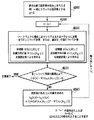
以下に、空間的な屈折率分布を決定するための一般的なアルゴリズムを説明する。図2に、波動伝達媒体の空間的な屈折率分布を決定するための計算手順を示す。この計算は、繰り返し実行されるので、繰り返し回数をqで表し、(q−1)番目まで計算が実行されているときのq番目の計算の様子が図示されている。(q−1)番目の計算によって得られた屈折率分布{nq-1}をもとに、各j番目の入射フィールドψj(x)および出射フィールドφj(x)について、伝搬フィールドと逆伝搬フィールドとを数値計算により求め、その結果を各々、ψj(z,x,{nq-1})およびφj(z,x,{nq-1})と表記する(ステップS220)。 In the following, a general algorithm for determining the spatial refractive index distribution will be described. FIG. 2 shows a calculation procedure for determining the spatial refractive index distribution of the wave transmission medium. Since this calculation is repeatedly executed, the number of repetitions is represented by q, and the state of the qth calculation when the calculation is executed up to the (q−1) th is shown. Based on the refractive index distribution {n q-1 } obtained by the (q-1) th calculation, the propagation field and the jth incident field ψ j (x) and the outgoing field φ j (x) The back propagation field is obtained by numerical calculation, and the results are expressed as ψ j (z, x, {n q-1 }) and φ j (z, x, {n q-1 }), respectively (step S220). ).
これらの結果をもとに、各場所(z,x)における屈折率nq(z,x)を、次式により求める(ステップS240)。
nq(z,x)=nq-1(z,x)−αΣjIm[φj(z,x,{nq-1})*・ψj(z,x,{nq-1})] ・・・(1)
ここで、右辺第2項中の記号「・」は、内積演算を意味し、Im[]は、[]内のフィールド内積演算結果の虚数成分を意味する。なお、記号「*」は複素共役である。係数αは、nq(z,x)の数分の1以下の値をさらにフィールドの組の数で割った値であり、正の小さな値である。Σjは、インデックスjについて和をとるという意味である。
Based on these results, the refractive index n q (z, x) at each location (z, x) is obtained by the following equation (step S240).
n q (z, x) = n q-1 (z, x) −αΣ j Im [φ j (z, x, {n q-1 }) * · ψ j (z, x, {n q-1 })] (1)
Here, the symbol “·” in the second term on the right side means an inner product operation, and Im [] means an imaginary number component of the field inner product operation result in []. The symbol “*” is a complex conjugate. The coefficient α is a value obtained by dividing a value equal to or less than a fraction of n q (z, x) by the number of field pairs, and is a small positive value. Σ j means that the sum is taken for the index j.
ステップS220とS240とを繰り返し、伝搬フィールドの出射面における値ψj(ze,x,{n})と出射フィールドφj(x)との差の絶対値が、所望の誤差djよりも小さくなると(ステップS230:YES)計算が終了する。 Step S220 and S240 and repeats the value in the exit plane of the propagation field ψ j (z e, x, {n}) the absolute value of the difference between the exit field φ j (x) is than desired error d j When it becomes smaller (step S230: YES), the calculation ends.
以上の計算では、屈折率分布の初期値{n0}は適当に設定すればよいが、この初期値{n0}が予想される屈折率分布に近ければ、それだけ計算の収束は早くなる(ステップS200)。また、各jについてφj(z,x,{nq-1})およびψj(z,x,{nq-1})を計算するにあたっては、パラレルに計算が可能な計算機の場合は、jごと(すなわち、φj(z,x,{nq-1})およびψj(z,x,{nq-1})ごと)に計算すればよいので、クラスタシステム等を利用して計算の効率化を図ることができる(ステップS220)。また、比較的少ないメモリで計算機が構成されている場合は、式(1)のインデックスjについての和の部分で、各qで適当なjを選び、その分のφj(z,x,{nq-1})およびψj(z,x,{nq-1})のみを計算して、以降の計算を繰り返すことも可能である(ステップS220)。 In the above calculation, the initial value {n 0 } of the refractive index distribution may be set appropriately. However, if this initial value {n 0 } is close to the expected refractive index distribution, the calculation converges faster accordingly ( Step S200). When calculating φ j (z, x, {n q-1 }) and ψ j (z, x, {n q-1 }) for each j, , J (that is, φ j (z, x, {n q-1 }) and ψ j (z, x, {n q-1 })). Thus, calculation efficiency can be improved (step S220). If the computer is configured with a relatively small memory, an appropriate j is selected for each q in the sum of the index j in equation (1), and φ j (z, x, { It is also possible to calculate only n q-1 }) and ψ j (z, x, {n q-1 }) and repeat the subsequent calculations (step S220).
以上の演算において、φj(z,x,{nq-1})の値とψj(z,x,{nq-1})の値とが近い場合には、式(1)中のIm[φj(z,x,{nq-1})*・ψj(z,x,{nq-1})]は位相差に対応する値となり、この値を減少させることで所望の出力を得ることが可能である。 In the above operation, φ j (z, x, {n q-1}) in the case of values and ψ j (z, x, { n q-1}) and the value of the near, the formula (1) Im [φ j (z, x, {n q-1 }) * · ψ j (z, x, {n q-1 })] is a value corresponding to the phase difference, and by reducing this value, It is possible to obtain a desired output.
屈折率分布の決定は、波動伝達媒体に仮想的メッシュを定め、このメッシュによって画定される微小領域(ピクセル)の屈折率を、各ピクセルごとに決定することと言い換えることもできる。このような局所的な屈折率は、原理的には、その場所ごとに任意の(所望の)値とすることができる。最も単純な系は、低屈折率(nL)を有するピクセルと高屈折率(nH)を有するピクセルのみからなる系であり、これら2種のピクセルの空間的分布により全体的な屈折率分布が決定される。この場合、媒体中の低屈折率ピクセルが存在する場所を高屈折率ピクセルの空隙として観念したり、逆に、高屈折率ピクセルが存在する場所を低屈折率ピクセルの空隙として観念したりすることができる。すなわち、本発明の波動伝達媒体は、均一な屈折率を有する媒体中の所望の場所(ピクセル)を、これとは異なる屈折率のピクセルで置換したものと表現することができる。 The determination of the refractive index distribution can be rephrased as defining a virtual mesh in the wave transmission medium and determining the refractive index of a minute region (pixel) defined by the mesh for each pixel. In principle, such a local refractive index can be an arbitrary (desired) value for each location. The simplest system is a system consisting only of pixels having a low refractive index (n L ) and pixels having a high refractive index (n H ), and the overall refractive index distribution due to the spatial distribution of these two types of pixels. Is determined. In this case, the place where the low refractive index pixel exists in the medium is considered as a gap of the high refractive index pixel, and conversely, the place where the high refractive index pixel exists is considered as the gap of the low refractive index pixel. Can do. That is, the wave transmission medium of the present invention can be expressed as a desired place (pixel) in a medium having a uniform refractive index replaced with a pixel having a different refractive index.
上述した屈折率分布決定のための演算内容を要約すると次のようになる。波動をホログラフィックに伝達させ得る媒体(光の場合には誘電体)に、入力ポートと出力ポートとを設け、入力ポートから入射した伝搬光のフィールド分布1(順伝搬光)と、入力ポートから入射した光信号が出力ポートから出力される際に期待される出力フィールドを出力ポート側から逆伝搬させた位相共役光のフィールド分布2(逆伝搬光)と、を数値計算により求める。フィールド分布1およびフィールド分布2を、伝搬光と逆伝搬光の各点(x,z)における位相差をなくすように、媒体中での空間的な屈折率分布を求める。なお、このような屈折率分布を得るための方法として最急降下法を採用すれば、各点の屈折率を変数として最急降下法により得られる方向に屈折率を変化させることにより、屈折率を式(1)のように変化させることで、2つのフィールド間の差を減少させることができる。このような波動伝達媒体を、入力ポートから入射した光を所望の出力ポートに出射させる光部品に応用すれば、媒体内で生じる伝搬波同士の多重散乱による干渉現象により、実効的な光路長が長くなり、緩やかな屈折率変化(分布)でも充分に高い光信号制御性を有する光回路を構成することができる。
The calculation contents for determining the refractive index distribution described above are summarized as follows. An input port and an output port are provided in a medium capable of transmitting a wave in a holographic manner (dielectric in the case of light). Field distribution 1 (forward propagation light) of propagating light incident from the input port and from the input port A field distribution 2 (reverse propagation light) of phase conjugate light in which an output field expected when an incident optical signal is output from the output port is propagated backward from the output port side is obtained by numerical calculation. In the
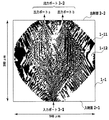
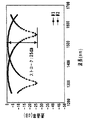
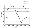
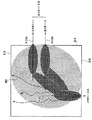
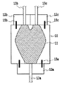
図3に、本発明の一実施形態にかかる光合分波回路を示す。上述したアルゴリズムにしたがって、約200回の繰り返しにより、図3に示した屈折率分布を有する1×2光合分波回路が得られる。ここで、図中の光回路設計領域1−1内の黒色部分は、コアに相当する高屈折率部(誘電体多重散乱部)1−11であり、黒色部以外の部分はクラッドに相当する低屈折率部1−12であり、導波路より屈折率の低い散乱点である。クラッドの屈折率は、石英ガラスの屈折率を想定し、コアの屈折率は、石英ガラスに対する比屈折率が1.5%だけ高い値を有する。光回路のサイズは縦300μm、横140μmである。屈折率分布を求める際の計算に用いられたメッシュは、300×140である。図4に、光合分波回路の透過スペクトルを示す。透過スペクトルから、波長による光合分波器が形成されていることがわかる。 FIG. 3 shows an optical multiplexing / demultiplexing circuit according to an embodiment of the present invention. According to the algorithm described above, the 1 × 2 optical multiplexing / demultiplexing circuit having the refractive index distribution shown in FIG. 3 is obtained by repeating about 200 times. Here, the black part in the optical circuit design region 1-1 in the figure is a high refractive index part (dielectric multiple scattering part) 1-11 corresponding to the core, and the part other than the black part corresponds to the clad. The low refractive index portion 1-12 is a scattering point having a refractive index lower than that of the waveguide. The refractive index of the clad assumes the refractive index of quartz glass, and the refractive index of the core has a value that is higher by 1.5% than the quartz glass. The size of the optical circuit is 300 μm in length and 140 μm in width. The mesh used for the calculation when obtaining the refractive index distribution is 300 × 140. FIG. 4 shows a transmission spectrum of the optical multiplexing / demultiplexing circuit. From the transmission spectrum, it can be seen that an optical multiplexer / demultiplexer according to wavelength is formed.
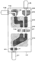
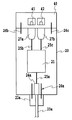
上述したように、ホログラフィック波動伝達媒体は、入力ポートから入射した光を所望の出力ポートに出射させることができる。そこで、基板上に複数の回路要素が形成された光機能回路において、各々の回路要素から漏れ出した光(以下、漏洩光という)、すなわち回路要素の所定の出力ポートから出射されない光を除去する光部品として、ホログラフィック波動伝達媒体を用いる。 As described above, the holographic wave transmission medium can emit light incident from the input port to a desired output port. Therefore, in an optical functional circuit in which a plurality of circuit elements are formed on a substrate, light leaked from each circuit element (hereinafter referred to as leaked light), that is, light not emitted from a predetermined output port of the circuit element is removed. A holographic wave transmission medium is used as the optical component.
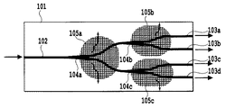
図5に、光分岐回路における漏洩光の除去方法を示す。1x4光分岐回路は、基板101に形成された導波路型の分岐回路であり、入力導波路102から入射された光は、3つの分岐導波路104a〜104cを透過して、4つの出力導波路103a〜103dから出射される。このとき、入出力導波路と光学的に結合する光ファイバの軸ズレ、モード不整合によって、1x4光分岐回路101内に漏洩光が生じる。また、分岐導波路104aにおいて生じる放射光またはエバネッセント光が漏洩光となって、分岐導波路104b,104c及び出力導波路103a〜103dに再結合して、分岐光の出力パワーの一様性を劣化させる。同様に、分岐導波路104b,104cにおいて生じた放射光またはエバネッセント光が漏洩光となって、出力導波路103a〜103dに再結合して分岐光の出力パワーの一様性を劣化させる。
FIG. 5 shows a method for removing leaked light in the optical branch circuit. The 1 × 4 optical branch circuit is a waveguide type branch circuit formed on the
そこで、分岐導波路104a〜104cにおいて生じる漏洩光が、導波路に再び結合することを防ぐために、迷光ガイド105a〜105cを設置する。迷光ガイド105a〜105cは、上述した波動伝達媒体であり、基板101内のクラッド部の有限の領域に配置されている。分岐導波路104a〜104cにおいて生じる漏洩光は、迷光ガイド105a〜105cにより、基板101の入出力導波路が形成されていない側面に出射される。
Therefore,
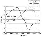
図6に、1x4光分岐回路の挿入損失を示す。波長1.55μmの光を入射したときの、入力導波路と各出力導波路との間の挿入損失を示す。迷光ガイド105a〜105cが有る場合の挿入損失のバラツキは0.1dBであり、迷光ガイドが無い場合の挿入損失バラツキは1dBである。波導伝達媒体を用いた迷光ガイドにより、漏洩光が除去されていることがわかる。
FIG. 6 shows the insertion loss of the 1 × 4 optical branch circuit. The insertion loss between the input waveguide and each output waveguide when light having a wavelength of 1.55 μm is incident is shown. The variation in insertion loss when the
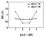
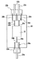
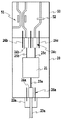
図7に、MZ型波長合分波回路における漏洩光の除去方法を示す。MZ型波長合分波回路は、入力導波路112a,112bに結合された光カプラ114aと、出力導波路113a,113bに結合された光カプラ114bと、光カプラ114aと光カプラ114bとを結合するアーム導波路116a,116bとから構成されている。実施例1同様に、入出力導波路と光学的に結合する光ファイバの軸ズレ、モード不整合によって、MZ型波長合分波回路内に漏洩光が生じる。また、光カプラ114a,114bにおいて生じる放射光またはエバネッセント光が漏洩光となって、アーム導波路116a,116b、出力導波路113a,113bに再結合してクロストークを劣化させる。
FIG. 7 shows a method for removing leakage light in the MZ type wavelength multiplexing / demultiplexing circuit. The MZ type wavelength multiplexing / demultiplexing circuit couples the
そこで、光カプラ114a,114bにおいて生じる漏洩光が、光導波路に再び結合することを防ぐために、迷光ガイド115a,115bを設置する。迷光ガイド115a,115bは、上述した波動伝達媒体であり、基板111内のクラッド部の有限の領域に配置されている。光カプラ114a,114bにおいて生じる漏洩光は、迷光ガイド115a,115bにより、基板111の入出力導波路が形成されていない側面に出射される。
Therefore, stray light guides 115a and 115b are installed in order to prevent leakage light generated in the
図8A,Bに、MZ型波長合分波回路の透過スペクトルを示す。図8Aは、迷光ガイドが無いMZ型波長合分波回路の透過スペクトルであり、クロストークは25dBである。図8Bは、実施例2にかかる漏洩光の除去方法を適用したMZ型波長合分波回路の透過スペクトルであり、クロストークは40dBである。波導伝達媒体を用いた迷光ガイド115a,115bにより、漏洩光が除去されていることがわかる。 8A and 8B show transmission spectra of the MZ type wavelength multiplexing / demultiplexing circuit. FIG. 8A is a transmission spectrum of an MZ type wavelength multiplexing / demultiplexing circuit without a stray light guide, and the crosstalk is 25 dB. FIG. 8B is a transmission spectrum of the MZ type wavelength multiplexing / demultiplexing circuit to which the leakage light removing method according to the second embodiment is applied, and the crosstalk is 40 dB. It can be seen that the leakage light is removed by the stray light guides 115a and 115b using the wave transmission medium.
実施例1,2では、ホログラフィック波動伝達媒体を、漏洩光を除去する光部品として適用することにより、従来の光回路において、複数の出力ポート間で干渉を生じず、透過損失、クロストークが小さいなど回路特性の良好な光機能回路を実現することが可能となる。 In the first and second embodiments, by applying the holographic wave transmission medium as an optical component that removes leakage light, in the conventional optical circuit, no interference occurs between a plurality of output ports, and transmission loss and crosstalk occur. It is possible to realize an optical functional circuit having a good circuit characteristic such as small.
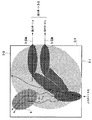
図4に示した光合分波回路の透過スペクトルを参照すると、出力ポートbに出射されるべき伝播光の一部が、出力ポートaに出射されていることがわかる。これは、メッシュ状の波動伝達媒体を作製する際の作製誤差により、波動伝達媒体を透過する光の一部が、所定の出力ポートには出力されず、他の出力ポートに出射されたり、出力ポート以外の部分から漏洩するからである。このように、入力ポートから入射された光信号のうち、所定の出力ポートから出射されない光、すなわち設計上想定された回路動作に寄与しない、または回路動作を阻害する伝播光を、以下「迷光」と呼ぶ。図4に示したように、出力ポートbに出射されるべき伝播光が、出力ポートaに迷光となって出射されていることがわかる。 Referring to the transmission spectrum of the optical multiplexing / demultiplexing circuit shown in FIG. 4, it can be seen that a part of the propagation light to be emitted to the output port b is emitted to the output port a. This is because part of the light transmitted through the wave transmission medium is not output to a predetermined output port, but is output to another output port or output due to a manufacturing error when manufacturing a mesh-shaped wave transmission medium. This is because leakage occurs from parts other than the port. In this way, among the optical signals incident from the input port, the light that is not emitted from the predetermined output port, that is, the propagation light that does not contribute to the circuit operation assumed in the design or hinders the circuit operation is hereinafter referred to as “stray light”. Call it. As shown in FIG. 4, it can be seen that the propagating light to be emitted to the output port b is emitted as stray light to the output port a.
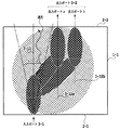
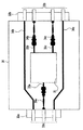
以下、この迷光の除去方法について、図3に示した光合分波回路を例として詳しく説明する。図9に、本発明の実施例3にかかる迷光の除去方法を示す。光合分波回路の入力ポート3−1の光軸3−11に対して、出力ポート3−2の光軸3−12a,bを座標x上で横方向にずらしている。具体的に図9を参照して、入力ポート3−1から入射された光信号のビーム広がり角の半値θとする。入力ポート3−1の光軸3−11に対して入力ポート3−1から角度θの2本の線と、出射面2−2との交点よりも外側に、出力ポート3−2を配置すればよい。 Hereinafter, the stray light removal method will be described in detail by taking the optical multiplexing / demultiplexing circuit shown in FIG. 3 as an example. FIG. 9 shows a method for removing stray light according to the third embodiment of the present invention. The optical axes 3-12a and b of the output port 3-2 are shifted laterally on the coordinate x with respect to the optical axis 3-11 of the input port 3-1 of the optical multiplexing / demultiplexing circuit. Specifically, referring to FIG. 9, it is assumed that the half value θ of the beam divergence angle of the optical signal incident from the input port 3-1. The output port 3-2 is disposed outside the intersection of the two lines having an angle θ from the input port 3-1 and the emission surface 2-2 with respect to the optical axis 3-11 of the input port 3-1. That's fine.
すなわち、設計上想定された回路動作に寄与しない伝播光成分は、屈折率の異なるピクセルによって散乱はされるものの、全体としてはほぼ直進するため、出力ポート3−2の光軸3−12a,bを、入力ポート3−1の光軸3−11に対して、ずらして設定するだけで、迷光を除去する一定の効果がある。 That is, although the propagation light component that does not contribute to the circuit operation assumed in the design is scattered by the pixels having different refractive indexes, it travels almost straight as a whole, so that the optical axes 3-12a and b of the output port 3-2. Is set to be shifted with respect to the optical axis 3-11 of the input port 3-1, and there is a certain effect of removing stray light.
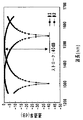
図10に、実施例3にかかる光合分波回路の透過スペクトルを示す。図4に示したスペクトルと比較すると、出力ポートaに出射されていた迷光が抑制されていることがわかる。このようにして、ホログラフィック波動伝達媒体を適用することにより小型化を実現することができ、複数の出力ポート間で干渉を生じず、透過損失、クロストークが小さいなど回路特性の良好な光機能回路を実現することができる。 FIG. 10 shows a transmission spectrum of the optical multiplexing / demultiplexing circuit according to the third example. Compared with the spectrum shown in FIG. 4, it can be seen that the stray light emitted to the output port a is suppressed. In this way, by applying a holographic wave transmission medium, it is possible to achieve miniaturization, no interference between multiple output ports, optical functions with good circuit characteristics such as low transmission loss and crosstalk A circuit can be realized.
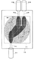
図11に、本発明の実施例4にかかる迷光の除去方法を示す。実施例3と同様に、入力ポート3−1の光軸3−11に対して、出力ポート3−2の光軸3−12a,bをずらす。実施例4では、出力ポート3−2を、x=xe上の出射面2−3に設定し、光軸3−11と光軸3−12a,bとが直角をなす。 FIG. 11 shows a method of removing stray light according to the fourth embodiment of the present invention. Similarly to the third embodiment, the optical axes 3-12a and b of the output port 3-2 are shifted with respect to the optical axis 3-11 of the input port 3-1. In Example 4, an output port 3-2, set the exit surface 2-3 of the x = x e, an optical axis 3-11 and the optical axis 3-12a, and a b perpendicular.
このとき、屈折率分布を求める計算は、入力ポート3−1と出力ポート3−2とを結ぶ直線に沿って計算すればよく、この場合には、入力フィールドと出力フィールドを傾けて与えることになる。 At this time, the refractive index distribution may be calculated along a straight line connecting the input port 3-1 and the output port 3-2. In this case, the input field and the output field are inclined and given. Become.
図12に、本発明の実施例5にかかる迷光の除去方法を示す。実施例4の構成に加えて、迷光ガイド4を配置する。実施例4では、入力ポートの光軸3−11に沿って、出射面2−2の方向に迷光が出力されると考えられる。そこで、光軸3−11周辺の迷光をまとめて、出射面2−2の左端部にまとめて出力できるように、迷光ガイド4を配置する。 FIG. 12 shows a method for removing stray light according to the fifth embodiment of the present invention. In addition to the configuration of the fourth embodiment, the stray light guide 4 is disposed. In the fourth embodiment, it is considered that stray light is output in the direction of the emission surface 2-2 along the optical axis 3-11 of the input port. Therefore, the stray light guide 4 is arranged so that stray light around the optical axis 3-11 can be collected and output to the left end portion of the emission surface 2-2.
迷光ガイド4の屈折率分布を求める計算は、迷光ガイドの入力端面を適当に決めて、入力端面での迷光フィールドを求める。次に、入力端面を基準とする軸に沿って、上述したアルゴリズムで計算を行う。 The calculation for obtaining the refractive index distribution of the stray light guide 4 appropriately determines the input end face of the stray light guide and obtains the stray light field at the input end face. Next, calculation is performed with the algorithm described above along an axis with the input end face as a reference.
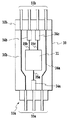
図13に、本発明の実施例6にかかる迷光の除去方法を示す。実施例3の構成に加えて、入力導波路5−1と出力導波路5−2a,bとを配置する。図9に示した光回路は、光回路設計領域1−1内に形成された波動伝達媒体の入力ポート3−1および出力ポート3−2が構造的な境界を有していないので、光ファイバとの接続が難しい。 FIG. 13 shows a method for removing stray light according to the sixth embodiment of the present invention. In addition to the configuration of the third embodiment, an input waveguide 5-1 and output waveguides 5-2a and b are disposed. In the optical circuit shown in FIG. 9, the input port 3-1 and the output port 3-2 of the wave transmission medium formed in the optical circuit design area 1-1 do not have a structural boundary. Connection with is difficult.
そこで、光回路設計領域1−1周辺の基板1−2に、入力ポートに接続された導波路5−1および出力ポートに接続された導波路5−2a,bを形成する。光導波路5−1,5−2は、コア部およびその周囲のクラッド部からなる直線導波路であり、構造的な境界を有しているので、光ファイバ6−1,6−2との接続が容易となる。 Therefore, the waveguide 5-1 connected to the input port and the waveguides 5-2a and b connected to the output port are formed on the substrate 1-2 around the optical circuit design region 1-1. The optical waveguides 5-1 and 5-2 are straight waveguides each including a core portion and a surrounding clad portion, and have a structural boundary. Therefore, the optical waveguides 5-1 and 6-2 are connected. Becomes easy.
なお、実施例6では、直線導波路を示したが、光導波路は、レイアウトに自在性があり、曲線導波路も可能である。従って、光回路設計領域1−1の入力ポートおよび出力ポートと、光ファイバとの位置関係の自由度が増す。 In the sixth embodiment, a straight waveguide is shown. However, the optical waveguide has a flexible layout, and a curved waveguide is also possible. Accordingly, the degree of freedom in the positional relationship between the optical fiber and the input port and output port of the optical circuit design area 1-1 is increased.
図14に、本発明の実施例7にかかる迷光の除去方法を示す。実施例7は、基板1−2の上に、図2に示した設計手順により設計された波動伝達媒体が形成された複数の光回路設計領域を有する複合光回路の一例である。光ファイバ6−1は、光回路設計領域1−1aの入力ポートに接続されている入力導波路5−1と光学的に結合されている。光回路設計領域1−1aは、例えば、光合分波器であり、2つの出力ポートを有する。出力ポートは、それぞれ接続導波路5−3a,bを介して、光回路設計領域1−1bの入力ポートに接続されている。光回路設計領域1−1bは、例えば、フィルタ回路であり、2つの出力ポートを有する。出力ポートは、それぞれ出力導波路5−2a,bを介して、光ファイバ6−2a,bに光学的に結合されている。 FIG. 14 shows a method of removing stray light according to the seventh embodiment of the present invention. Example 7 is an example of a composite optical circuit having a plurality of optical circuit design regions in which a wave transmission medium designed by the design procedure shown in FIG. 2 is formed on a substrate 1-2. The optical fiber 6-1 is optically coupled to the input waveguide 5-1 connected to the input port of the optical circuit design area 1-1a. The optical circuit design area 1-1a is an optical multiplexer / demultiplexer, for example, and has two output ports. The output port is connected to the input port of the optical circuit design area 1-1b via connection waveguides 5-3a and b, respectively. The optical circuit design area 1-1b is a filter circuit, for example, and has two output ports. The output ports are optically coupled to the optical fibers 6-2a and b via output waveguides 5-2a and b, respectively.
光回路設計領域1−1aは、実施例3に示したように、入力ポートの光軸に対して、出力ポートの光軸が座標x上で横方向にずれている。入力導波路5−1の周囲には、実施例5と同様に、光ファイバと入力導波路との接続部で発生する迷光が、光回路設計領域1−1aに入力されないように、迷光ガイド4−2を配置する。 In the optical circuit design area 1-1 a, as shown in the third embodiment, the optical axis of the output port is shifted laterally on the coordinate x with respect to the optical axis of the input port. As in the fifth embodiment, the stray light guide 4 is provided around the input waveguide 5-1 so that stray light generated at the connection portion between the optical fiber and the input waveguide is not input to the optical circuit design area 1-1a. -2.
また、導波路5−3a,bの周囲には、出力ポートと導波路との接続部で発生する迷光が、光回路設計領域1−1bに入力されないように、迷光ガイド4−3を配置する。出力導波路5−2a,bの周囲にも、出力ポートと導波路との接続部で発生する迷光が、光ファイバに結合しないように、迷光ガイド4−4a,bを配置する。 A stray light guide 4-3 is arranged around the waveguides 5-3a and b so that stray light generated at the connection portion between the output port and the waveguide is not input to the optical circuit design region 1-1b. . Stray light guides 4-4a and 4b are also arranged around the output waveguides 5-2a and b so that stray light generated at the connection between the output port and the waveguide is not coupled to the optical fiber.
このようにして、接続部で発生する迷光、波動伝達媒体で発生する迷光が、次段の光回路に入力されないようにして、各々回路特性のよい光回路を構成することができる。また、ホログラフィック波動伝達媒体を適用することにより光回路の小型化を実現することができる。 In this way, it is possible to configure an optical circuit with good circuit characteristics so that stray light generated in the connection portion and stray light generated in the wave transmission medium are not input to the optical circuit in the next stage. Further, by applying a holographic wave transmission medium, the optical circuit can be reduced in size.
実施例3〜7では、ホログラフィック波動伝達媒体を適用することにより光回路の小型化を図り、さらに、入力ポートの光軸と出力ポートの光軸とが、互いに一致しないように配置することにより、複数の出力ポート間で干渉を生じず、透過損失、クロストークが小さいなど回路特性の良好な光機能回路を実現することが可能となる。 In the third to seventh embodiments, the optical circuit is downsized by applying a holographic wave transmission medium, and further, the optical axis of the input port and the optical axis of the output port are arranged so as not to coincide with each other. Thus, it is possible to realize an optical functional circuit having good circuit characteristics such as no interference between a plurality of output ports, small transmission loss and crosstalk.
上述したように、入出力導波路と光学的に結合する光ファイバの軸ズレ、モード不整合によって、漏洩光が生じたり、迷光が発生する。そこで、ホログラフィック波動伝達媒体を適用した光導波路デバイスの接続を容易にして、透過損失、クロストークが小さい光機能回路を実現する。 As described above, leakage light or stray light is generated due to axial misalignment and mode mismatch of the optical fiber optically coupled to the input / output waveguide. Therefore, it is possible to easily connect an optical waveguide device to which a holographic wave transmission medium is applied, thereby realizing an optical functional circuit with small transmission loss and crosstalk.
図15に、本発明の実施例8にかかる光合分波回路を含む光導波路デバイスの構成を示す。図3に示した光合分波回路に光ファイバを接続し、不図示のパッケージに封入することにより光導波路デバイスを構成する。基板10に形成された波動伝達媒体11の入射端面における入力ポートと、出射端面における出力ポートとに、光ファイバ13a〜13cの端面を結合する。光ファイバ13a〜13cは、固定するガラスブロック12a〜12cに固定され、基板10とガラスブロック12a〜12cとの位置合わせを行いながら入出力ポートに結合する。
FIG. 15 shows a configuration of an optical waveguide device including an optical multiplexing / demultiplexing circuit according to the eighth embodiment of the present invention. An optical waveguide device is configured by connecting an optical fiber to the optical multiplexing / demultiplexing circuit shown in FIG. 3 and enclosing it in a package (not shown). The end faces of the
波動伝達媒体11は、メッシュ状のピクセルのため、構造的な境界を有していないので、入出力ポートの集光位置を目視で判別することが困難である。そこで、基板10には、演算の際に決定された入出力ポートの座標を基準に、調芯用のマーカ15a〜15cを形成する。調芯用マーカ15a〜15cは、基板10に導波路コアを形成しても良いし、基板10表面に金属を形成するなどしても良い。対向するガラスブロック12a〜12cにも、光ファイバ23a〜23cの集光位置に対応したマーカを形成しておくことにより、位置あわせを容易に行うことができる。
Since the
図16に、本発明の実施例9にかかる光合分波回路を含む光導波路デバイスの構成を示す。入出力ポート近傍の光のビーム径が小さい領域において、光の進行方向に対して斜めに入射する成分の割合を小さくして、クロストークを抑える必要がある。そこで、図3に示した光合分波回路である波動伝達媒体21の入力ポートに導波路25aを接続し、出力ポートに光導波路25b,25cを接続する。さらに、基板20には、モードフィールド変換用の波動伝達媒体24a〜24cを形成して、光導波路25a〜25cと光ファイバ23a〜23cとの結合効率を向上させる。
FIG. 16 shows a configuration of an optical waveguide device including an optical multiplexing / demultiplexing circuit according to Example 9 of the present invention. In the region where the beam diameter of light in the vicinity of the input / output port is small, it is necessary to suppress the crosstalk by reducing the ratio of the component incident obliquely with respect to the light traveling direction. Therefore, the
モードフィールド変換用の波動伝達媒体24a〜24cと光ファイバ23a〜23cとの接続においても、調芯用のマーカ26a〜26cを用いる。すなわち、基板20には、演算の際に決定された入出力ポートの座標を基準に、調芯用マーカ26a〜26cを形成し、対向するガラスブロック22a,22bにも、光ファイバ23a〜23cの集光位置に対応したマーカを形成しておくことにより、位置あわせを容易に行うことができる。
The
図17に、本発明の実施例10にかかる光合分波回路を含む光導波路デバイスの構成を示す。実施例9との相違は、モードフィールド変換用の波動伝達媒体24a〜24cの構成が異なる。
FIG. 17 shows a configuration of an optical waveguide device including an optical multiplexing / demultiplexing circuit according to Example 10 of the present invention. The difference from the ninth embodiment is the configuration of the
実施例9の波動伝達媒体24a〜24cは、仮想的なメッシュにより画定される仮想的なピクセルの各々が有する屈折率(ここでは、2値の屈折率)により、波動伝達媒体の全体的な屈折率分布を決定していた。実施例10では、上述した空間的な屈折率分布を決定するための一般的なアルゴリズムを使用して、図17に示すように、光導波路のコア幅を光軸方向に変調することにより屈折率分布を決定する。
The
波動伝達媒体24aのコアの幅の構成方法について簡単に説明する。光ファイバ23aから入力された信号光のフィールドと、波動伝達媒体21に出力される希望の信号光のフィールドの位相を反転させたフィールドを、光ファイバ23aへ伝搬させたフィールドとの位相差が、最小となるような屈折率分布を与えれば、入力させた信号光を希望の出力信号光に変換することができる。具体的には、光軸方向の各位置における位相差を計算し、位相差が正である場合には光導波路のコア幅を拡大し、位相差が負である場合には光導波路のコア幅を縮小することにより位相差を最小化する。このような構成方法に基づき、位相差が最小となるような光導波路のコアの幅をそれぞれ計算により求めることで、入力させた信号光を希望の出力信号光に変換することができる。
A method of configuring the core width of the
図18に、本発明の実施例11にかかる光合分波回路を含む光導波路デバイスの構成を示す。図3に示した光合分波回路である波動伝達媒体21が形成された基板20と、発光素子41と受光素子42とが載置された基板40とを結合して、不図示のパッケージに封入することにより光導波路デバイスを構成する。波動伝達媒体21の出力ポートに光導波路25b,25cを接続し、集光レンズとなる波動伝達媒体27a〜27bを形成して、発光素子41および受光素子42との結合効率を向上させる。
FIG. 18 shows the configuration of an optical waveguide device including an optical multiplexing / demultiplexing circuit according to Example 11 of the present invention. The
集光レンズとなる波動伝達媒体27a〜27bと発光素子41および受光素子42との接続においても、調芯用のマーカ26b,26cを用いる。このようにして、集光レンズを波動伝達媒体として基板上に形成することで、光導波路デバイスの小型化を図ることができる。従来、光導波路デバイスを作製する際に、発光素子および受光素子と、集光レンズと、光合分波器との間で光軸合わせが必要であったが、本実施形態によれば、調芯用のマーカによる位置合わせを行うだけなので、光導波路デバイスの作製工程を短縮することができる。
The
図19に、本発明の実施例12にかかる光合分波回路を含む光導波路デバイスの構成を示す。図3に示した光合分波回路である波動伝達媒体21が形成された基板20と、例えば、光スイッチ51と光フィルタ52とが形成された基板50とを結合して、不図示のパッケージに封入することにより光導波路デバイスを構成する。基板20の光導波路25b,25cと基板50の光導波路とを、モードフィールド変換用の波動伝達媒体24b,24cにより接続する。
FIG. 19 shows a configuration of an optical waveguide device including an optical multiplexing / demultiplexing circuit according to Example 12 of the present invention. The
接続のための位置合わせには、図16の光ファイバの場合と同様に、調芯用のマーカ26b,26cを用いる。このようにして、従来のPLC回路と波動伝達媒体との接続も、調芯用のマーカにより容易に行うことができ、実施例8,9と本実施例によれば、様々な構成の光導波路デバイスを容易に組み合わせることができる。
For alignment for connection,
図20に、本発明の実施例13にかかる光合分波回路を含む光導波路デバイスの構成を示す。基板30上の波動伝達媒体31の入力ポートには導波路35aを接続し、出力ポートには光導波路35b,35cを接続する。実施例9と同様に、さらに、モードフィールド変換用の波動伝達媒体34a〜34cを形成して、光導波路35a〜35cと入出力用の光ファイバ33a,33bとの結合効率を向上させる。
FIG. 20 shows the configuration of an optical waveguide device including an optical multiplexing / demultiplexing circuit according to Example 13 of the present invention. The
モードフィールド変換用の波動伝達媒体34a〜34cと入出力用の光ファイバ33a,33bとの接続には、モニタ用導波路36a,36bを用いる。すなわち、基板30には、演算の際に決定された入出力ポートの座標を基準に、モニタ用導波路36a,36bのポートを形成し、対向するガラスブロック32a,32bにも、光ファイバの集光位置に対応した調芯用の光ファイバ33a,33bを保持しておく。調芯用の光ファイバ33a,33bとモニタ用導波路36a,36bとを介して、光源と光パワーメータを接続し、光強度を測定しながら接続位置をきめることにより、モードフィールド変換用の波動伝達媒体34a〜34cと入出力用の光ファイバ33a,33bとの位置あわせを容易に行うことができる。
図21に、本発明の実施例14にかかる光合分波回路を含む光導波路デバイスの構成を示す。実施例13との相違は、モードフィールド変換用の波動伝達媒体34a〜34cが、実施例10と同様に、導波路幅を変調した波動伝達媒体となっている。
FIG. 21 shows a configuration of an optical waveguide device including an optical multiplexing / demultiplexing circuit according to Example 14 of the present invention. The difference from the thirteenth embodiment is that
実施例8〜14では、基板上に形成された調芯用のマーカまたはモニタ用導波路により、ホログラフィック波動伝達媒体を適用した光導波路デバイスの接続を容易にすることが可能となる。 In Examples 8 to 14, it is possible to easily connect an optical waveguide device to which a holographic wave transmission medium is applied by using an alignment marker or a monitoring waveguide formed on a substrate.
図22に、本発明の実施例15にかかる光回線終端装置(ONU)の構成を示す。ONUは、光ファイバ加入者網の加入者宅に設置される機器であり、局側の光回線終端装置(OLT)との間で、光信号の送受信を行う。OLT−ONUの下り信号には、波長1.55μmを使用し、ONU−OLTの上り信号には、波長1.55μmを使用する。
FIG. 22 shows a configuration of an optical network unit (ONU) according to
ONUは、PLC基板201上に下り信号を受信するPD202と、上り信号を送信するLD203と、LD203の出力光のパワーを監視するモニタPD204と、上り信号および下り信号を合分波するWDMフィルタ205とを備えている。また、WDMフィルタ205で波長多重された信号は、ガラスブロック206に固定された光ファイバ207を介して、OLTと接続される。ONUにおいては、PD202と光導波路、LD203と光導波路、WDMフィルタ205と光導波路、光ファイバ207と光導波路との接続箇所において、漏洩光が生じる。
The ONU includes a
そこで、上述した実施例に記載された漏洩光の除去方法などを適用する。波動伝達体211,212は、実施例11に示したように、集光レンズの機能を有し、それぞれPD202と光導波路、LD203と光導波路の結合効率を向上させる。WDMフィルタと光導波路の交差箇所においては、実施例1,2に示したように、波動伝達体からなる迷光ガイド213a,213bを設置して、漏洩光が再び光導波路に結合することを防ぐ。さらに、PLC基板201とガラスブロック206との接続には、実施例8に示したように、マーカ215a,215bを用い、光ファイバ207と光導波路との結合には、実施例9に示したように、モードフィールド変換用の波動伝達媒体214を用いる。
Therefore, the leakage light removal method described in the above-described embodiment is applied. As shown in the eleventh embodiment, the
このようにして、各々の接続箇所における光結合の結合効率を向上させるとともに、クロストークを抑制することにより、光受信器としてS/Nの劣化を回避することができる。また、実装工程における接続が容易になるので、実装のための工数削減し、生産性を向上することができる。 In this way, it is possible to avoid S / N degradation as an optical receiver by improving the coupling efficiency of optical coupling at each connection location and suppressing crosstalk. Further, since the connection in the mounting process becomes easy, man-hours for mounting can be reduced and productivity can be improved.
Claims (3)
前記光の伝搬方向に垂直な断面において、前記光のフィールドの断面が与えられるべき回路上の場所をポートとし、任意の1個のポートから入射された入力光が、所定のポートから出力光として出射されるように、前記コア層に空間的な屈折率分布が形成された第1の波動伝達媒体を備え、
前記第1の波動伝達媒体の前記所定のポートから出射されない漏洩光が、他の回路要素と結合しないように、入力光として入力ポートから入射された前記漏洩光が、光路を変換されて、出力ポートから出力光として出射されるように、前記コア層に空間的な屈折率分布が形成された第2の波動伝達媒体を備え、
前記空間的な屈折率分布は、前記第1の波動伝達媒体の前記入力光が、前記任意の1個のポートから前記光の伝搬方向に沿って伝搬すると、前記入力光の入力フィールドが、前記出力光の出力フィールドに変換されて、前記所定のポートから出力される1つ以上の入出力フィールドの組の各々を伝搬するように、および前記第2の波動伝達媒体の前記入力光が、前記入力ポートから前記光の伝搬方向に沿って伝搬すると、前記入力光の入力フィールドが、前記出力光の出力フィールドに変換されて、前記出力ポートから出力される1つ以上の入出力フィールドの組の各々を伝搬するように、メッシュにより画定されるピクセルの各々のコアが有する屈折率によって決定され、
各々の前記ピクセルのコアの屈折率は、前記任意の1個のポートまたは前記入力ポートから前記所定のポートまたは前記出力ポートまでの光の伝搬方向の座標z、前記光の導波領域において前記光の伝搬方向に垂直な方向の座標xとしたときの断面Xの場所(z,x)において、前記入力フィールドの順伝搬のフィールドの位相と、前記出力フィールドの位相共役に逆伝搬させたフィールドの位相との間の位相差が所定の誤差以下となるように、各々の前記ピクセルのコアの屈折率を変数として繰り返し計算を行うことにより決定され、この計算は、(q−1)番目の計算によって得られた屈折率分布{nq -1}をもとに、前記入出力フィールドの組のj番目の入力フィールドψj(x)および出力フィールドφj(x)について、前記順伝搬フィールドψj(z,x,{nq -1})と前記逆伝搬のフィールドφj(z,x,{nq -1})としたとき、各場所(z,x)における屈折率nq(z,x)を、
nq(z,x)=nq -1(z,x)−αΣjIm[φj(z,x,{nq -1})*・ψj(z,x,{nq -1})]
として計算し、ここで、記号「*」は複素共役であり、記号「・」は内積演算であり、Im[]は[]内のフィールド内積演算結果の虚数成分であり、αは計算の収束を考慮した定数であり、Σjはjについて和を示し、かつ、
前記入力光のフィールドが、前記任意の1個のポートまたは前記入力ポートから前記所定のポートまたは前記出力ポートまでの伝搬方向に沿って、前記断面Xの屈折率分布により位相の変化を多段に受けることにより、前記第1および第2波動伝達媒体内で生じる伝搬波同士の多重散乱による干渉現象により光のフィールドの形状を変化させながら伝搬して、前記所定のポートまたは前記出力ポートから前記出力光の出力フィールドとして出射されることを特徴とする光機能回路。In an optical functional circuit in which a light waveguide region including a cladding layer and a core layer having a higher refractive index than the cladding layer embedded in the cladding layer is provided on a substrate,
In a cross section perpendicular to the light propagation direction, a place on the circuit to which a cross section of the light field is to be given is defined as a port, and input light incident from any one port is output as light from a predetermined port. A first wave transmission medium having a spatial refractive index distribution formed in the core layer so as to be emitted;
The leaked light incident from the input port as input light is converted in an optical path so that the leaked light not emitted from the predetermined port of the first wave transmission medium is not coupled with other circuit elements, and is output. A second wave transmission medium in which a spatial refractive index distribution is formed in the core layer so as to be emitted as output light from the port;
The spatial refractive index distribution is such that when the input light of the first wave transmission medium propagates along the light propagation direction from the arbitrary one port, the input field of the input light is The input light of the second wave transmission medium is converted into an output field of output light and propagated through each of one or more sets of input / output fields output from the predetermined port, Propagating along the light propagation direction from the input port, the input field of the input light is converted into the output field of the output light, and a set of one or more input / output fields output from the output port Determined by the refractive index of each core of the pixels defined by the mesh to propagate through each,
The refractive index of the core of each pixel is a coordinate z of light propagation direction from the arbitrary one port or the input port to the predetermined port or the output port, and the light in the light guiding region. In the position (z, x) of the cross section X when the coordinate x is in the direction perpendicular to the propagation direction, the phase of the forward propagation field of the input field and the phase of the field propagated back to the phase conjugate of the output field This is determined by repeatedly performing calculation using the refractive index of the core of each pixel as a variable so that the phase difference from the phase is equal to or less than a predetermined error, and this calculation is the (q-1) th calculation. based on the obtained refractive index distribution {n q -1} by the the input and output fields of the set of j-th input field [psi j (x) and the output field phi j (x), the forward propagation feel ψ j (z, x, { n q -1}) and the inverse propagation field φ j (z, x, { n q -1}) when the refractive index n q at each location (z, x) (Z, x)
n q (z, x) = n q -1 (z, x) −αΣ j Im [φ j (z, x, {n q −1 }) * · ψ j (z, x, {n q −1 })]
Where the symbol “*” is a complex conjugate, the symbol “•” is an inner product operation, Im [] is the imaginary component of the field inner product operation result in [], and α is the convergence of the calculation Where Σ j is the sum for j, and
The field of the input light undergoes a multi-stage phase change by the refractive index distribution of the cross section X along the propagation direction from the arbitrary one port or the input port to the predetermined port or the output port. As a result, the light propagates while changing the shape of the light field due to the interference phenomenon caused by the multiple scattering of the propagation waves generated in the first and second wave transmission media, and the output light from the predetermined port or the output port. The optical functional circuit is emitted as an output field.
Applications Claiming Priority (5)
| Application Number | Priority Date | Filing Date | Title |
|---|---|---|---|
| JP2004197313 | 2004-07-02 | ||
| JP2004197313 | 2004-07-02 | ||
| JP2004317092 | 2004-10-29 | ||
| JP2004317092 | 2004-10-29 | ||
| PCT/JP2005/012186 WO2006004031A1 (en) | 2004-07-02 | 2005-07-01 | Optical functional circuit |
Publications (2)
| Publication Number | Publication Date |
|---|---|
| JPWO2006004031A1 JPWO2006004031A1 (en) | 2007-08-16 |
| JP4113236B2 true JP4113236B2 (en) | 2008-07-09 |
Family
ID=35782835
Family Applications (1)
| Application Number | Title | Priority Date | Filing Date |
|---|---|---|---|
| JP2006523769A Expired - Lifetime JP4113236B2 (en) | 2004-07-02 | 2005-07-01 | Optical functional circuit |
Country Status (6)
| Country | Link |
|---|---|
| US (1) | US7580597B2 (en) |
| EP (1) | EP1764635B1 (en) |
| JP (1) | JP4113236B2 (en) |
| KR (1) | KR100799659B1 (en) |
| CA (1) | CA2552417C (en) |
| WO (1) | WO2006004031A1 (en) |
Families Citing this family (4)
| Publication number | Priority date | Publication date | Assignee | Title |
|---|---|---|---|---|
| JP4625420B2 (en) * | 2006-04-04 | 2011-02-02 | 日本電信電話株式会社 | Optical circuit |
| JP5071542B2 (en) * | 2010-09-30 | 2012-11-14 | 住友大阪セメント株式会社 | Optical waveguide device |
| CN116802533A (en) * | 2021-01-29 | 2023-09-22 | 京瓷株式会社 | Optical circuit board and electronic component mounting structure using the same |
| US20240411157A1 (en) * | 2023-06-12 | 2024-12-12 | X Development Llc | Inverse designed photonic integrated circuit with improved signal to noise ratio |
Family Cites Families (17)
| Publication number | Priority date | Publication date | Assignee | Title |
|---|---|---|---|---|
| JPS60202553A (en) * | 1984-03-27 | 1985-10-14 | Nec Corp | Waveguide path type optical head |
| JP2773990B2 (en) | 1991-04-15 | 1998-07-09 | 日本碍子株式会社 | Method for manufacturing combined body of optical waveguide substrate and optical fiber alignment substrate |
| JPH0511135A (en) * | 1991-07-01 | 1993-01-19 | Furukawa Electric Co Ltd:The | How to connect optical fiber and optical waveguide |
| JP2002031731A (en) | 1993-08-09 | 2002-01-31 | Nippon Telegr & Teleph Corp <Ntt> | Hybrid optical integrated circuit |
| JPH08190028A (en) | 1995-01-12 | 1996-07-23 | Hitachi Cable Ltd | NxM splitter waveguide element and method of manufacturing the same |
| JP3151699B2 (en) | 1995-05-18 | 2001-04-03 | 日本電信電話株式会社 | Fabrication method of optical circuit components |
| JP3765140B2 (en) * | 1996-12-19 | 2006-04-12 | 富士ゼロックス株式会社 | Optical bus and signal processing device |
| JPH10332966A (en) * | 1997-06-03 | 1998-12-18 | Nippon Telegr & Teleph Corp <Ntt> | Optical device |
| US6618535B1 (en) * | 2001-04-05 | 2003-09-09 | Nortel Networks Limited | Photonic bandgap device using coupled defects |
| US7373045B2 (en) | 2001-07-03 | 2008-05-13 | Brown University Research Foundation | Method and apparatus for processing optical signals with supergratings |
| US7116851B2 (en) * | 2001-10-09 | 2006-10-03 | Infinera Corporation | Optical signal receiver, an associated photonic integrated circuit (RxPIC), and method improving performance |
| JP2003344677A (en) | 2002-05-29 | 2003-12-03 | Fujitsu Ltd | Photonic crystal optical waveguide |
| JP2004046021A (en) * | 2002-07-15 | 2004-02-12 | Omron Corp | Optical waveguide device, optical multiplexing / demultiplexing device, and optical wavelength division multiplexing transmission device |
| JP2004163731A (en) | 2002-11-14 | 2004-06-10 | Seiko Epson Corp | Optical device and manufacturing method thereof |
| US7397977B2 (en) * | 2002-12-26 | 2008-07-08 | Nippon Telegraph And Telephone Corporation | Wave transmission medium and waveguide circuit |
| US7489846B2 (en) * | 2004-03-11 | 2009-02-10 | Agilent Technologies, Inc. | Photonic crystal sensors |
| JP2005352453A (en) * | 2004-05-12 | 2005-12-22 | Nec Corp | Optical fiber component, optical waveguide module, and manufacturing method |
-
2005
- 2005-07-01 EP EP05755862.9A patent/EP1764635B1/en not_active Expired - Lifetime
- 2005-07-01 KR KR1020067012952A patent/KR100799659B1/en not_active Expired - Lifetime
- 2005-07-01 WO PCT/JP2005/012186 patent/WO2006004031A1/en not_active Ceased
- 2005-07-01 US US10/584,820 patent/US7580597B2/en not_active Expired - Lifetime
- 2005-07-01 JP JP2006523769A patent/JP4113236B2/en not_active Expired - Lifetime
- 2005-07-01 CA CA002552417A patent/CA2552417C/en not_active Expired - Lifetime
Also Published As
| Publication number | Publication date |
|---|---|
| US7580597B2 (en) | 2009-08-25 |
| WO2006004031A1 (en) | 2006-01-12 |
| EP1764635B1 (en) | 2018-04-25 |
| EP1764635A4 (en) | 2010-08-04 |
| CA2552417A1 (en) | 2006-01-12 |
| JPWO2006004031A1 (en) | 2007-08-16 |
| EP1764635A1 (en) | 2007-03-21 |
| KR100799659B1 (en) | 2008-01-30 |
| CA2552417C (en) | 2010-03-09 |
| US20080232736A1 (en) | 2008-09-25 |
| KR20060111624A (en) | 2006-10-27 |
Similar Documents
| Publication | Publication Date | Title |
|---|---|---|
| CA2511944C (en) | Wave transmission medium and waveguide circuit | |
| WO2013046696A1 (en) | Light merging/branching device, bidirectional light propagation device, and light transmission/reception system | |
| JP3726062B2 (en) | Optical multiplexer / demultiplexer | |
| US9151901B2 (en) | Wavelength-selective path-switching element | |
| Zhang et al. | Scalable and low crosstalk silicon mode exchanger for mode division multiplexing system enabled by inverse design | |
| JP4383815B2 (en) | Method for manufacturing holographic wave transmission medium | |
| JP4113236B2 (en) | Optical functional circuit | |
| US20020006249A1 (en) | Bragg grating assisted mmimi-coupler for tunable add-drop multiplexing | |
| JP2014182213A (en) | Optical element | |
| CN100399079C (en) | Optical functional circuit | |
| JP2006030687A (en) | Waveguide type optical multiplexer / demultiplexer | |
| JP3851314B2 (en) | Optical branch circuit, optical transceiver circuit and optical network | |
| JP4069102B2 (en) | Waveguide type optical multiplexer / demultiplexer | |
| JP4113161B2 (en) | Optical waveguide switch | |
| JP4069101B2 (en) | Waveguide type optical multiplexer / demultiplexer | |
| JP5118772B2 (en) | Optical interconnect | |
| JP2006126658A (en) | Optical waveguide device | |
| JP2003270460A (en) | Integrated optical circuit including arrayed waveguide grating type wavelength multiplexer / demultiplexer. | |
| KR20020008455A (en) | Low loss Multi Mode Interferometer for optical distributer and Wavelength division Multiplexer module | |
| JP4113162B2 (en) | Optical waveguide and method for manufacturing the same | |
| Huang | Silicon photonic switching: from building block design to intelligent control | |
| JP2006039053A (en) | Optical functional circuit | |
| JP4126268B2 (en) | Arrayed waveguide grating type optical multiplexer / demultiplexer | |
| JP2006039052A (en) | Optical functional circuit | |
| JP2006058499A (en) | Optical waveguide device |
Legal Events
| Date | Code | Title | Description |
|---|---|---|---|
| A131 | Notification of reasons for refusal |
Free format text: JAPANESE INTERMEDIATE CODE: A131 Effective date: 20070622 |
|
| A521 | Request for written amendment filed |
Free format text: JAPANESE INTERMEDIATE CODE: A523 Effective date: 20070821 |
|
| A131 | Notification of reasons for refusal |
Free format text: JAPANESE INTERMEDIATE CODE: A131 Effective date: 20070918 |
|
| A521 | Request for written amendment filed |
Free format text: JAPANESE INTERMEDIATE CODE: A523 Effective date: 20071119 |
|
| A131 | Notification of reasons for refusal |
Free format text: JAPANESE INTERMEDIATE CODE: A131 Effective date: 20071228 |
|
| A521 | Request for written amendment filed |
Free format text: JAPANESE INTERMEDIATE CODE: A523 Effective date: 20080226 |
|
| TRDD | Decision of grant or rejection written | ||
| A01 | Written decision to grant a patent or to grant a registration (utility model) |
Free format text: JAPANESE INTERMEDIATE CODE: A01 Effective date: 20080404 |
|
| A61 | First payment of annual fees (during grant procedure) |
Free format text: JAPANESE INTERMEDIATE CODE: A61 Effective date: 20080410 |
|
| R151 | Written notification of patent or utility model registration |
Ref document number: 4113236 Country of ref document: JP Free format text: JAPANESE INTERMEDIATE CODE: R151 |
|
| FPAY | Renewal fee payment (event date is renewal date of database) |
Free format text: PAYMENT UNTIL: 20110418 Year of fee payment: 3 |
|
| FPAY | Renewal fee payment (event date is renewal date of database) |
Free format text: PAYMENT UNTIL: 20120418 Year of fee payment: 4 |
|
| FPAY | Renewal fee payment (event date is renewal date of database) |
Free format text: PAYMENT UNTIL: 20130418 Year of fee payment: 5 |
|
| FPAY | Renewal fee payment (event date is renewal date of database) |
Free format text: PAYMENT UNTIL: 20140418 Year of fee payment: 6 |
|
| S531 | Written request for registration of change of domicile |
Free format text: JAPANESE INTERMEDIATE CODE: R313531 |
|
| R350 | Written notification of registration of transfer |
Free format text: JAPANESE INTERMEDIATE CODE: R350 |
|
| EXPY | Cancellation because of completion of term |