JP4061019B2 - 導電性緩衝中間層構造を有する炭化ケイ素基質上の第iii族窒化物フォトニックデバイス - Google Patents
導電性緩衝中間層構造を有する炭化ケイ素基質上の第iii族窒化物フォトニックデバイス Download PDFInfo
- Publication number
- JP4061019B2 JP4061019B2 JP2000515300A JP2000515300A JP4061019B2 JP 4061019 B2 JP4061019 B2 JP 4061019B2 JP 2000515300 A JP2000515300 A JP 2000515300A JP 2000515300 A JP2000515300 A JP 2000515300A JP 4061019 B2 JP4061019 B2 JP 4061019B2
- Authority
- JP
- Japan
- Prior art keywords
- silicon carbide
- carbide substrate
- gallium nitride
- group iii
- buffer layer
- Prior art date
- Legal status (The legal status is an assumption and is not a legal conclusion. Google has not performed a legal analysis and makes no representation as to the accuracy of the status listed.)
- Expired - Lifetime
Links
Images


Classifications
-
- H—ELECTRICITY
- H01—ELECTRIC ELEMENTS
- H01L—SEMICONDUCTOR DEVICES NOT COVERED BY CLASS H10
- H01L33/00—Semiconductor devices with at least one potential-jump barrier or surface barrier specially adapted for light emission; Processes or apparatus specially adapted for the manufacture or treatment thereof or of parts thereof; Details thereof
- H01L33/005—Processes
- H01L33/0062—Processes for devices with an active region comprising only III-V compounds
- H01L33/0066—Processes for devices with an active region comprising only III-V compounds with a substrate not being a III-V compound
- H01L33/007—Processes for devices with an active region comprising only III-V compounds with a substrate not being a III-V compound comprising nitride compounds
-
- H—ELECTRICITY
- H01—ELECTRIC ELEMENTS
- H01L—SEMICONDUCTOR DEVICES NOT COVERED BY CLASS H10
- H01L21/00—Processes or apparatus adapted for the manufacture or treatment of semiconductor or solid state devices or of parts thereof
- H01L21/02—Manufacture or treatment of semiconductor devices or of parts thereof
- H01L21/02104—Forming layers
- H01L21/02365—Forming inorganic semiconducting materials on a substrate
- H01L21/02367—Substrates
- H01L21/0237—Materials
- H01L21/02373—Group 14 semiconducting materials
- H01L21/02378—Silicon carbide
-
- H—ELECTRICITY
- H01—ELECTRIC ELEMENTS
- H01L—SEMICONDUCTOR DEVICES NOT COVERED BY CLASS H10
- H01L21/00—Processes or apparatus adapted for the manufacture or treatment of semiconductor or solid state devices or of parts thereof
- H01L21/02—Manufacture or treatment of semiconductor devices or of parts thereof
- H01L21/02104—Forming layers
- H01L21/02365—Forming inorganic semiconducting materials on a substrate
- H01L21/02436—Intermediate layers between substrates and deposited layers
- H01L21/02439—Materials
- H01L21/02455—Group 13/15 materials
- H01L21/02458—Nitrides
-
- H—ELECTRICITY
- H01—ELECTRIC ELEMENTS
- H01L—SEMICONDUCTOR DEVICES NOT COVERED BY CLASS H10
- H01L21/00—Processes or apparatus adapted for the manufacture or treatment of semiconductor or solid state devices or of parts thereof
- H01L21/02—Manufacture or treatment of semiconductor devices or of parts thereof
- H01L21/02104—Forming layers
- H01L21/02365—Forming inorganic semiconducting materials on a substrate
- H01L21/02436—Intermediate layers between substrates and deposited layers
- H01L21/02494—Structure
- H01L21/02513—Microstructure
-
- H—ELECTRICITY
- H01—ELECTRIC ELEMENTS
- H01L—SEMICONDUCTOR DEVICES NOT COVERED BY CLASS H10
- H01L21/00—Processes or apparatus adapted for the manufacture or treatment of semiconductor or solid state devices or of parts thereof
- H01L21/02—Manufacture or treatment of semiconductor devices or of parts thereof
- H01L21/02104—Forming layers
- H01L21/02365—Forming inorganic semiconducting materials on a substrate
- H01L21/02518—Deposited layers
- H01L21/02521—Materials
- H01L21/02538—Group 13/15 materials
- H01L21/0254—Nitrides
-
- H—ELECTRICITY
- H01—ELECTRIC ELEMENTS
- H01L—SEMICONDUCTOR DEVICES NOT COVERED BY CLASS H10
- H01L21/00—Processes or apparatus adapted for the manufacture or treatment of semiconductor or solid state devices or of parts thereof
- H01L21/02—Manufacture or treatment of semiconductor devices or of parts thereof
- H01L21/02104—Forming layers
- H01L21/02365—Forming inorganic semiconducting materials on a substrate
- H01L21/02612—Formation types
- H01L21/02617—Deposition types
- H01L21/02636—Selective deposition, e.g. simultaneous growth of mono- and non-monocrystalline semiconductor materials
- H01L21/02639—Preparation of substrate for selective deposition
- H01L21/02642—Mask materials other than SiO2 or SiN
Description
発明の分野
本発明は禁止帯の幅が広い物質におけるフォトニックデバイスに関し、とくに炭化ケイ素基質に第III族窒化物活性層を形成させたフォトニックデバイスに関する。
発明の背景
ダイアモンド、炭化ケイ素、および窒化ガリウムのような禁止帯の幅が広い半導体物質は、その幅広い禁止帯の特徴がヒ化ケイ素またはヒ化ガリウムのような他の半導体よりも高エネルギー(したがって高周波及び短波長を有する)の光を発する可能性を該半導体にもたらすために近年著しい関心が寄せられている。とくに、炭化ケイ素、窒化ガリウム、及びある種の他の第III族窒化物は高エネルギーの青色の部分を含む可視スペクトル全般に可視光を生じるだけの大きい禁止帯幅を有する。従ってこれらは青及び緑色の発光を有する半導体レーザー及び発光ダイオード(LEDs)の基礎となる。
【0002】
これらの物質中で窒化ガリウムは直接遷移形半導体であり、すなわち価電子帯から伝導帯への遷移が電子のための結晶運動量を必要としないのでとくに関心がある。その結果、遷移は極めて効率的に光を生じる。対照的に炭化ケイ素は間接遷移形半導体であり、禁止帯幅の遷移エネルギーは一部はフォトンとして、そして一部は振動エネルギーとして放出される。したがって、窒化ガリウムは一定の動作電圧及び電流に対して炭化ケイ素よりも効果的に光を生じるという利点を与える。
【0003】
しかし他の半導体物質と同様に、使用可能なフォトニックデバイスを形成させる第1工程は所望の活性層を有する適当な結晶構造を作り上げるか、または入手することである。しかし半導体物質の構造上の特徴の差によって、使用できるように第III族窒化物活性層デバイスを支持する材料は幾分限られる。
【0004】
現在発光ダイオードフォトニックデバイス用の市販構造はサファイア基質上に窒化ガリウム又は類似第III族窒化物活性層を形成させる。サファイア(Al2O3)は第III族窒化物に対して比較的密な格子整合を与えるが、やはりある欠点を生じ、その最も極端であるのは電気的絶縁性である。したがってサファイア上に第III族窒化物活性及び緩衝層(すなわち基質から活性層へ結晶構造の遷移をもたらす中間層)を形成させる場合に、サファイアはデバイスの活性部分への導電通路として用いることができない。これはサファイア上に設計して作ることができるデバイスの種類を制限し、とくにデバイスの接点をデバイスの反対面に置いて、基質、緩衝、および活性層間の直接導電通路とすることができる「垂直」デバイスを形成させる能力を制限する。
【0005】
したがって、本発明出願人を含めて第III族窒化物フォトニックデバイスの基質候補者として他の物質の使用に関心が集められている。炭化ケイ素(SiC)は導電性にすることができるのでとくに魅力的な候補者であり、第III族窒化物活性層に適切に緩衝させることができる格子整合(lattice match)を有し、そして優れた熱的及び機械的安定性を有する。
【0006】
それにもかかわらず、炭化ケイ素の結晶格子構造は炭化ケイ素基質上の適当な第III族緩衝層の最良の候補者の中にあって導電性では無くて絶縁性であるようなものである。したがって、炭化ケイ素基質を導電性にすることができるけれども、炭化ケイ素基質と第III族活性層フォトニックデバイスとの間の好ましい緩衝層の一部は絶縁性のままであり、したがって導電性炭化ケイ素基質の利点を最小限にする。
【0007】
たとえば、窒化アルミニウム(AlN)は炭化ケイ素基質と第III族活性層とくに窒化ガリウム活性層との間の優れた緩衝をもたらす。しかし窒化アルミニウムは導電性ではなくて絶縁性である。したがって、窒化アルミニウム緩衝層を有する構造は窒化アルミニウム緩衝をバイパスして導電性炭化ケイ素基質を第III族窒化物活性層に電気的に連結させる短接点(shorting contact)が必要である。上記のようにこのような短接点はより有利なデバイス設計の幾分かを妨げる。
【0008】
もしくは、窒化ガリウム(GaN),窒化アルミニウムガリウム(AlGaN)または窒化ガリウムと窒化アルミニウムガリウムとの混合物のような導電性緩衝層物質は短接点を無くすことができる。さらに、短接点を無くすことはエピタキシャル層の厚さを減じ、デバイスを作るのに必要な加工工程数を減少させ、全般的なチップの大きさを小さくし、そしてデバイスの効率を向上させる。したがって、第III族窒化物デバイスは低コストで作ることができて優れた性能を発揮させることができる。
【0009】
それにも拘わらず、これら導電性緩衝物質はこれらの利点を付与するけれども、その炭化ケイ素との結晶格子整合は窒化アルミニウムの場合ほど満足できない。それゆえ、窒化ガリウム、窒化アルミニウムガリウム、またはこれらの混合物のエピタキシャル緩衝層を炭化ケイ素基質上に成長させる場合には、発光ダイオードまたはレーザーダイオードのようなフォトニックデバイスに必要な次のエピ層に過度の破壊を生じやすい。
【0010】
したがって、窒化アルミニウムの結晶格子整合の利点を与え、しかもなお同時に窒化ガリウム又は窒化アルミニウムガリウムの導電性の利点を与え、さらに絶縁性サファイア基質ではなくて導電性炭化ケイ素基質とともに使用できる緩衝構造に対する要望が存在する。
発明の目的及び要約
したがって、本発明の目的は、第III族窒化物活性層、導電性炭化ケイ素基質、および導電性緩衝層を有するが、該物質および層を今日まで妨げて来た破壊及び他の問題を無くしたフォトニックデバイス及びそのウェーハー前駆物質を製造することにある。
【0011】
本発明は、炭化ケイ素基質、第III族窒化物活性層を有するオプトエレクトロニックダイオード、および炭化ケイ素基質とオプトエレクトロニックダイオードとの間の緩衝構造(該緩衝構造は導電性であると同時に適当な結晶性を与える)を含む第III族窒化物活性層を有するフォトニックデバイスの場合にこの目的を満足させる。
【0012】
1つの態様において、緩衝構造は窒化ガリウム及び窒化インジウムガリウム(InGaN)からなる群から選ばれ、そして緩衝層内で生じる応力誘発破壊が緩衝層中の他の部分では無くて所定の領域に生じるように、緩衝層の結晶構造内に複数の所定応力除去領域を含む応力吸収構造を包含する。
【0013】
別の態様では、緩衝層は炭化ケイ素と窒化アルミニウムガリウム緩衝構造との間のヘテロバリヤーを最小にするかまたは無くすために炭化ケイ素基質表面に窒化ガリウム及び窒化インジウムガリウムからなる群から選ばれる複数の不連続結晶部分を包含する。
【0014】
本発明の前記及び他の目的及び利点は添付詳細な説明および図面と合わせ考えればより明らかになろう。
詳細な説明
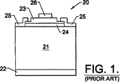
図1は大まかに20で表す先行技術のデバイスの断面図である。図1に示すように、デバイス20は炭化ケイ素基質21、基質21の「背面」への接点22、第III族窒化物活性層23、導電性ではなくて絶縁性である緩衝層24、導電性ケイ素緩衝21及び活性層23との間の電気接点となる短接点25、および回路を完成して動作中にデバイス全体に電流を流させる上面接点26を含む。
【0015】
図2は本発明がよりコンパクトなデバイスをもたらす態様を示す。図2において、デバイスは大まかに30で表され、導電性炭化ケイ素基質31、背面接点32、活性層33および導電性緩衝構造34、ならびに上面接点35を含む。したがってこの発明は図1のデバイスの短接点(典型的には環状短接点)25を無くしている。その結果デバイス30は作りやすく、また操作上効率がよい。本発明で述べる活性層33がシングルp−n接合、シングルまたはダブルp−nヘテロ接合もしくはp−n接合量子ウェル構造を有するデバイスを表すことができることは理解されよう。該構造は米国特許第5,393,993号および第5,592,501号を含む多くの先行米国特許に記載されており、本発明をさらに説明する以外に別にここで詳しく述べる必要はない。
【0016】
図3は本発明によるデバイス30が大まかに40で表される三色ピクセル(さらにディスプレー41中の複数の該ピクセルの1つであることができる)の一部として異なる発光波長の類似のデバイス、とくに赤色発光ダイオード36及び緑色発光ダイオードを備えることができることを示す。図4に図示される垂直線42及び水平線43は発光ダイオードを含むディスプレーで典型的に用いられるピクセルの行及び列を表す。
【0017】
第1の態様において、本発明は、炭化ケイ素基質31、第III族窒化物活性層を有するフォトニックダイオード33、および炭化ケイ素基質31とダイオード33との間の窒化ガリウム及び窒化インジウムガリウムからなる群から選ばれる緩衝構造34を含む第III族窒化物活性層を有するフォトニックデバイスである。とくに、緩衝構造は、緩衝構造内に生じる応力誘発破壊が構造中の他の部分では無くて所定の領域に生じるように緩衝構造34の結晶構造内に複数の所定の応力除去領域からなる応力吸収構造を包含する。
【0018】
図5は複数のデバイス前駆物質を具備し、かつ本発明の応力吸収構造を具備するウェーハーの略図である。図5は溝45のグリッドパターンを重ねた大まかに44で表されるウェーハーを示す。図6は横断面配列状の同じウェーハー44及び溝45を示す。溝45を有するウェーハー44上に次のエピタキシャル層46(図7)を成長させると、エピタキシャル層46の表面は一連の不連続47を有する傾向があり、その位置はウェーハー44中にパターンを形成する溝45の位置を再現する。この不連続47は緩衝層46の結晶格子構造が炭化ケイ素ウェーハー44上に成長するにつれて応力が除去される領域を形成する。その結果、格子不整合(または他の要因)に起因するような応力はランダムな位置ではなくて意図された位置に生じ、したがって著しい応力破壊の恐れなしに残りの領域にデバイスを形成させることができる。
【0019】
上記及び図5に示すように、1つの好ましい態様において、応力除去領域の所定のパターンはグリッドを含み、そのグリッドは好ましくは個々のデバイスを形成する所望または必要なサイズに形成させることができる。たとえば、個々のデバイスが発光ダイオードである場合には、好ましいグリッドパターンは一辺当たり約250ミクロンの正方形を形成する。若しくは、レーザーダイオードのような異なるデバイスの場合には、グリッドは約250×500ミクロン(μ)の矩形を形成することができる。
【0020】
図10は、(幾分三角形または六角形のパターンのように見える)破壊がエピタキシャル層を損ない、そしてフォトニックデバイスとしては欠陥品または使用できないものとなる程度を示す倍率10(実際の大きさの10倍)で撮ったSEM写真である。
【0021】
図11は別の倍率10のSEM写真であって、エピタキシャル層中の溝のグリッドパターンを示す。図10と比べると、図11に見られる表面は破壊欠陥が比較的存在しない。
【0022】
図12は別の倍率10のSEM写真であって、さらに小さいグリッドパターンを示す。図11と同様に、図10に見られた破壊が全く存在しない。
【0023】
図13はとくに本発明の利点を示す倍率50のSEM写真である。図13では、グリッド部分の1つが大きな欠陥(幾分“X”状の)を含んでいる。しかしこの欠陥はグリッド線で終わり、ウェーハーの複数のデバイス部分では無くてわずか1つのデバイス(またはデバイス前駆物質)を損なうだけである。
【0024】
図14は、欠陥がさらに表面全体に広がらずにグリッド線で終わるために同様に1つの欠陥グリッド部分(写真の右下部分)を示す倍率100のSEM写真である。
【0025】
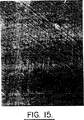
図15は本発明のいずれの態様も含まない表面を示す倍率100のSEM写真である。図10と同様に、欠陥の幾何学的パターンがかなり明らかである。
【0026】
他の態様において、応力吸収構造が、図8及び9においてもっともよく示される小さなメサ構造の所定のパターンを含むことができる。図8および9において、炭化ケイ素基質は50で表され、小さなメサ構造は51で表される。メサ構造51は選ばれた緩衝物質の成長が嫌われる物質からなる。窒化ガリウムまたは窒化インジウムガリウム緩衝構造の場合には、好ましい物質は二酸化ケイ素、窒化ケイ素、および酸化アルミニウムからなる群から選ばれる。
【0027】
図9は図8と同じ構造を示すが、ただし炭化ケイ素基質50上に緩衝物質をエピタキシャル層として成長させている。エピタキシャル層部分は52で表す。図9に示すように、メサ51上では緩衝物質の成長が嫌われるので、エピタキシャル層52は、その間に所定の応力除去不連続構造を示すパターンを形成する。前記態様と同様に、メサ間の面積を、前記のようにLEDの場合には約250ミクロン、レーザーダイオードの場合には約250×500μのオーダーにある個々のデバイスとほゞ同じ大きさに合わせることができる。しかし、グリッドまたはメサ構造のいずれかのパターンの特定サイズは本発明を限定するものではなくて例示的なものであることは理解されよう。
【0028】
本発明によるウェーハー構造はオプトエレクトロニックデバイスにはとくに有利であるけれども、該構造はそれに限定されないで、その優れた構造性はウェーハーに形成される他のデバイスにとっても有利であることを理解されたい。
【0029】
バックグラウンドの部分に認められるように、緩衝層上に形成されるオプトエレクトロニックデバイスは、典型的に図1の23および図2の33で示すように、通常単一層ではなくて、むしろp−nホモ接合、p−nヘテロ接合、p−nシングル及びダブルヘテロ接合、ならびにp−n接合量子ウェル構造からなる群から選ばれる多層ダイオードである。
【0030】
好ましい態様では、炭化ケイ素基質は3C、4H、6H、および15Rポリタイプからなる群から選ばれるポリタイプを有する。もっとも好ましい態様では、ダイオードの第III族窒化物活性層は窒化ガリウムまたは窒化インジウムガリウムを含む。
【0031】
図16ないし17は本発明の他の態様を説明する。概して、略図的に全般的な構造は図2でも示されるが、炭化ケイ素基質31、フォトニックダイオード33および緩衝層34を含む。しかしこの態様において、緩衝層は窒化ガリウムまたは窒化インジウムガリウムではなくて窒化アルミニウムガリウムである。この態様は図16−17において白点として見える複数の不連続結晶部分を含む。不連続結晶部分は窒化ガリウム及び窒化インジウムガリウムの群から選ばれ、炭化ケイ素基質31と窒化アルミニウムガリウム緩衝構造34との間のヘテロバリヤーを最小にするかまたは無くすために炭化ケイ素基質表面にある。
【0032】
好ましい態様では不連続結晶部分は、ヘテロバリヤーを最小にするかまたは無くすだけの量であるが、炭化ケイ素基質31に形成して出来たダイオードデバイスの機能に悪影響を与えるか又は破壊すると思われる量よりは少ない量で存在する。図16−17の写真に示すように、不連続結晶部分は平方ミクロン当たり約40ないし60個存在する。
【0033】
さらに、不連続結晶部分のサイズはヘテロバリヤーを最小にするかまたは無くす程大きいが、炭化ケイ素基質31に形成させたダイオードデバイスの機能に悪影響を与えるかまたは破壊すると思われるサイズよりは小さいのが好ましい。好ましい態様では、不連続結晶部分は直径が0.01ないし0.1ミクロンである。
【0034】
前記態様と同様に、緩衝構造に形成されたオプトエレクトロニックデバイス33は発光ダイオードまたはレーザーダイオードを含むことができ、生成発光ダイオードはピクセルに組み込まれることができ、ピクセルはさらにディスプレーに組み込まれることができる。
【0035】
好ましい態様では、窒化アルミニウムガリウム緩衝層は約10ないし15%の原子分率のアルミニウムを有する。
【0036】
別の態様では、本発明は、導電性緩衝構造を有する炭化ケイ素基質上に第III族窒化物オプトエレクトロニックデバイスを生成させる方法を含む。その方法態様において、本発明は結晶を成長させるために別に調製した炭化ケイ素基質表面に構造パターンを形成させ;炭化ケイ素基質表面の開口部のパターンに従う特徴を表すように炭化ケイ素基質のパターン化表面に窒化ガリウム及び窒化インジウムガリウムなる群から選ばれる緩衝層を形成させ;さらにその後緩衝層に第III族窒化物活性層を有するオプトエレクトロニックデバイスを形成させることを含む。
【0037】
構造態様について述べたように、構造パターンを形成させる工程は炭化ケイ素基質表面に開口部のパターンを形成させるかまたは炭化ケイ素基質表面にメサ構造のパターンを形成させることができる。
【0038】
パターンが開口部を形成するときには、開口部を形成する工程は反応性イオンエッチングまたはマスキング及びエッチング工程のような方法を含むことができる。これらの工程はいずれも炭化ケイ素について比較的よく理解されており、炭化ケイ素についてドライエッチング法を例示する例えば米国特許第4,865,685号および第4,981,551号に言及する以外に別に述べる必要はない。
【0039】
メサ構造を具体化する場合には、該構造を二酸化ケイ素、窒化ケイ素、及び酸化アルミニウムからなり群から選ぶのが好ましい。構造環境の場合のように、第III族活性層を有するオプトエレクトロニックデバイスは窒化ガリウムまたは窒化インジウムガリウムからなるのが好ましい。
【0040】
構造態様におけるように、本発明の方法は発光ダイオードまたはレーザーダイオードを形成させることを含み、そして発光を形成させるときには、該方法はさらにLEDをピクセルに組み込み、ピクセルをディスプレーに組み込むことを含むことができる。
【0041】
別の方法態様では、炭化ケイ素表面に窒化ガリウム及び窒化インジウムガリウムからなる群から選ばれる複数の不連続結晶部分を形成させることによってあらかじめ調製した炭化ケイ素基質に窒化アルミニウムガリウムの本発明の緩衝構造を形成させる。その後緩衝層に第III族窒化物活性層を形成させる。
【0042】
本発明の構造態様で述べたように、該方法はヘテロバリヤーを最小にするかまたは無くすだけのサイズ及び量ではあるが、炭化ケイ素基質に形成して出来たダイオードデバイスの機能に悪影響を与えるかまたは破壊すると思われるサイズまたは量以下である不連続結晶部分を形成させることを含む。とくに本発明は通常予想されるレベルの静電放電に耐えることができるロバスト(robust)構造を付与する。
【0043】
第2の方法態様では、得られたデバイスを発光ダイオードとして作ることが出来、該方法はさらにLEDピクセルを組み込み、該ピクセルをディスプレーに組み込むことができる。該方法はLEDではなくてレーザーダイオードをつくることを含むことができる。
【0044】
本発明の他の態様と同様に、窒化アルミニウムガリウム緩衝層を用いる場合には、該層が約10ないし15%の原子分率のアルミニウムを有することが好ましい。
実施例
導電性緩衝LEDおよびレーザーダイオードを生成させる現行法では、まずGaNドットを付着させる。GaNドットの目的はSiC基質およびSiドープAlGaN緩衝層間のバリヤーを減少させることである。これは構造中の他のエピタキシャル層に用いられるよりもかなり低い温度で行われる。静電放電が悪影響を与えないようにドットを比較的小さく保つことが重要である。GaNドットは約6秒で付着させ、さらにSiドープAl10Ga90Nで約15秒間「キャッピング」する。このキャッピングの目的は加熱時の GaNの解離を防ぐことである。この材料システムにおいて、NH3/H2雰囲気中ではAlGaNはGaNよりも安定であるので、AlのGaNへの添加、すなわちAl(1-x)Ga(x)Nは物質の解離速度を減少させる。ドットのキャッピング後、温度を緩衝層温度までランプ(ramp)させる。ランプ後緩衝層の成長が始まる前に約2分間温度を安定させる。
【0045】
特定実験において、NH3およびH2雰囲気中でそれぞれ13SLMおよび15SLMにおいて、SiCウェーハーを加熱する。GaNドット、AlGaNキャッピング、および続く緩衝層の成長の間これらのフローを一定に維持する。GaNドットの温度が約900℃に達するまで10分間にわたりランプさせる。系内の温度を約5分間安定させた後、約6秒間10−15ccのトリメチルガリウムを流すことによって(TMG;−5℃,600torr)ドットを付着させる。ドットを確実に導電性とするために、TMGフローとともにSiHをも加える。SiH4の量は約1×1018cm-3のキャリヤー濃度でGaNバルク層を成長させることによって測定する。GaNドットの付着直後、TMGおよびSiH4を流し続けるが、この場合にはトリメチルアルミニウムを添加する(TMA,92cc,25℃,600torr)。これは約10−11%AlGaNの「キャッピング」をもたらす。キャップの成長時間は15秒である。フロー(TMG,TMAおよびSiH4)を停止して温度を典型的に約1060℃である緩衝温度にランプさせる。温度ランプは1秒で、温度を安定化させる間2分間続ける。緩衝層はさらに成長させる。典型的な条件は18ccTMG/110ccTMA/.087ccSiH4である。緩衝層はほゞ11−12%AlGaNからなり、厚さは典型的に約1600ないし2700Åである。
【0046】
本発明の典型的な態様は図面および明細書で開示され、そして特定な用語を用いているけれども、それらは単に一般的で説明するための意味で用いられ、限定するためのものではなく、本発明の範囲は次のクレームに示されている。
【図面の簡単な説明】
【図1】 図1は環状短接点を有する先行技術のダイオードの断面図である。
【図2】 図2は本発明によって生成させることができる垂直ダイオードの断面図である。
【図3】 図3は本発明によって形成されるピクセルの拡大略図である。
【図4】 図4は本発明による構造を包含する複数のピクセルを含むディスプレーの略図である。
【図5】 図5は本発明による応力除去構造を包含する炭化ケイ素ウェーハーの略図である。
【図6】 図6は図5のウェーハーの断面図である。
【図7】 図7は図5のウェーハーの断面図で、ウェーハー上に成長した緩衝層を略図で示す。
【図8】 図8は本発明の第2の態様を取り入れたウェーハーの断面図である。
【図9】 図9は図8と同一の断面図であるが、ウェーハー上の補足的結晶成長を示す。
【図10】 図10は本発明を取り入れないエピ層の走査型電子顕微鏡(SEM)による倍率10の写真である。
【図11】 図11は本発明によるエピ層を示す倍率10のSEM写真である。
【図12】 図12は本発明によるエピ層を示す別の倍率10のSEM写真である。
【図13】 図13は図12と類似のエピ層の倍率50のSEM写真である。
【図14】 図14は本発明によるエピ層の倍率100のSEM写真である。
【図15】 図15は本発明を取り入れない他のエピ層を示すず別の倍率100のSEM写真である。
【図16】 図16は本発明の第2の態様の倍率15,000のSEM写真である。
【図17】 図17は第2の態様の倍率50,000のSEM写真である。
Claims (12)
- 第III族窒化物デバイスのウェーハー前駆物質であって、炭化ケイ素基質表面に所定パターンの溝を含む前記炭化ケイ素基質;
前記炭化ケイ素基質上の緩衝層で、前記緩衝層が窒化ガリウムおよび窒化インジウムガリウムからなる群から選ばれる;および
応力誘発破壊が緩衝構造内の他の場所ではなくて前記所定パターンに沿って前記緩衝層内に生じることにより、応力誘発破壊の程度を小さくするように、前記基質の前記所定パターンの溝に追随する位置において前記緩衝層内に成長した複数の応力吸収結晶不連続性を含む
ウェーハー前駆物質。 - 前記所定パターンが一辺当たり250ミクロンの正方形を形成するグリッド又は250×500ミクロンの矩形を形成するグリッドのいずれかである請求項1記載のウェーハー前駆物質。
- 第III族窒化物活性層を有するオプトエレクトロニックダイオードを含む請求項2記載の該ウェーハー前駆物質から形成されるオプトエレクトロニックデバイス。
- 前記ダイオードがp−nホモ接合、p−nシングルおよびダブルヘテロ接合、ならびにp−n量子接合ウェル構造からなる群から選ばれ、そして前記炭化ケイ素基質が3C、4H、6H、および15Rポリタイプからなる群から選ばれるポリタイプを有する請求項3記載のオプトエレクトロニックデバイス。
- 前記第III族窒化物活性層が窒化ガリウム及び窒化インジウムガリウムから選ばれる請求項3記載のオプトエレクトロニックデバイス。
- 発光ダイオードを含む請求項3記載のオプトエレクトロニックデバイス。
- 請求項6記載の発光ダイオードを包含するピクセル。
- 請求項7記載の複数のピクセルを包含するディスプレー。
- レーザーダイオードを含む請求項3記載のオプトエレクトロニックデバイス。
- 炭化ケイ素基質上に第III族窒化物オプトエレクトロニックデバイスを生成させる方法であって、
該炭化ケイ素基質上に結晶を成長させるために別の方法で調製された炭化ケイ素基質表面に所定パターンの溝を形成させ;
緩衝層が、該炭化ケイ素基質表面の所定パターンに追従する該緩衝層の結晶構造において応力吸収不連続性を成長し、それによって成長中に結晶内のクラックを最小にするように、該炭化ケイ素基質のパターン化された表面に窒化ガリウム及び窒化インジウムガリウムからなる群から選ばれる緩衝層を形成させ;そして
該緩衝層に第III族窒化物活性層を有するオプトエレクトロニックデバイスを形成させる
ことを含む方法。 - 該溝を形成させる工程が、該炭化ケイ素基質の表面をマスキングし、その後該表面をエッチングして該パターンを生成させることを含む請求項10記載の方法。
- 第III族窒化物活性層を有するオプトエレクトロニックデバイスを形成させる工程が、窒化ガリウムおよび窒化インジウムガリウムからなる群から選ばれる活性層を有するデバイスを形成させることを含む請求項10記載の方法。
Applications Claiming Priority (3)
| Application Number | Priority Date | Filing Date | Title |
|---|---|---|---|
| US08/944,547 US6201262B1 (en) | 1997-10-07 | 1997-10-07 | Group III nitride photonic devices on silicon carbide substrates with conductive buffer interlay structure |
| US08/944,547 | 1997-10-07 | ||
| PCT/US1998/021160 WO1999018617A1 (en) | 1997-10-07 | 1998-10-06 | Group iii nitride photonic devices on silicon carbide substrates with conductive buffer interlayer structure |
Related Child Applications (1)
| Application Number | Title | Priority Date | Filing Date |
|---|---|---|---|
| JP2006349833A Division JP4966645B2 (ja) | 1997-10-07 | 2006-12-26 | 導電性緩衝中間層構造を有する炭化ケイ素基質上の第iii族窒化物フォトニックデバイス |
Publications (3)
| Publication Number | Publication Date |
|---|---|
| JP2001519603A JP2001519603A (ja) | 2001-10-23 |
| JP2001519603A5 JP2001519603A5 (ja) | 2005-05-26 |
| JP4061019B2 true JP4061019B2 (ja) | 2008-03-12 |
Family
ID=25481617
Family Applications (2)
| Application Number | Title | Priority Date | Filing Date |
|---|---|---|---|
| JP2000515300A Expired - Lifetime JP4061019B2 (ja) | 1997-10-07 | 1998-10-06 | 導電性緩衝中間層構造を有する炭化ケイ素基質上の第iii族窒化物フォトニックデバイス |
| JP2006349833A Expired - Lifetime JP4966645B2 (ja) | 1997-10-07 | 2006-12-26 | 導電性緩衝中間層構造を有する炭化ケイ素基質上の第iii族窒化物フォトニックデバイス |
Family Applications After (1)
| Application Number | Title | Priority Date | Filing Date |
|---|---|---|---|
| JP2006349833A Expired - Lifetime JP4966645B2 (ja) | 1997-10-07 | 2006-12-26 | 導電性緩衝中間層構造を有する炭化ケイ素基質上の第iii族窒化物フォトニックデバイス |
Country Status (8)
| Country | Link |
|---|---|
| US (5) | US6201262B1 (ja) |
| EP (1) | EP1027736A1 (ja) |
| JP (2) | JP4061019B2 (ja) |
| KR (1) | KR100592897B1 (ja) |
| CN (1) | CN1185719C (ja) |
| AU (1) | AU9689098A (ja) |
| CA (1) | CA2305203C (ja) |
| WO (1) | WO1999018617A1 (ja) |
Families Citing this family (328)
| Publication number | Priority date | Publication date | Assignee | Title |
|---|---|---|---|---|
| US6403708B2 (en) | 1996-05-27 | 2002-06-11 | Mitsui Chemicals Inc | Crystalline polypropylenes, process for preparing thereof, polypropylene compositions, and thermoformed products |
| JP3060973B2 (ja) * | 1996-12-24 | 2000-07-10 | 日本電気株式会社 | 選択成長法を用いた窒化ガリウム系半導体レーザの製造方法及び窒化ガリウム系半導体レーザ |
| AU747260B2 (en) | 1997-07-25 | 2002-05-09 | Nichia Chemical Industries, Ltd. | Nitride semiconductor device |
| JP3283802B2 (ja) * | 1997-09-29 | 2002-05-20 | 日本電気株式会社 | 選択成長法を用いた半導体層及びその成長方法、選択成長法を用いた窒化物系半導体層及びその成長方法、窒化物系半導体発光素子とその製造方法 |
| US6201262B1 (en) * | 1997-10-07 | 2001-03-13 | Cree, Inc. | Group III nitride photonic devices on silicon carbide substrates with conductive buffer interlay structure |
| US6265289B1 (en) | 1998-06-10 | 2001-07-24 | North Carolina State University | Methods of fabricating gallium nitride semiconductor layers by lateral growth from sidewalls into trenches, and gallium nitride semiconductor structures fabricated thereby |
| US6606335B1 (en) * | 1998-07-14 | 2003-08-12 | Fujitsu Limited | Semiconductor laser, semiconductor device, and their manufacture methods |
| JP5080820B2 (ja) * | 1998-07-31 | 2012-11-21 | シャープ株式会社 | 窒化物半導体構造とその製造方法および発光素子 |
| US6459100B1 (en) * | 1998-09-16 | 2002-10-01 | Cree, Inc. | Vertical geometry ingan LED |
| JP3770014B2 (ja) | 1999-02-09 | 2006-04-26 | 日亜化学工業株式会社 | 窒化物半導体素子 |
| EP1168539B1 (en) | 1999-03-04 | 2009-12-16 | Nichia Corporation | Nitride semiconductor laser device |
| US6812053B1 (en) | 1999-10-14 | 2004-11-02 | Cree, Inc. | Single step pendeo- and lateral epitaxial overgrowth of Group III-nitride epitaxial layers with Group III-nitride buffer layer and resulting structures |
| US6380108B1 (en) | 1999-12-21 | 2002-04-30 | North Carolina State University | Pendeoepitaxial methods of fabricating gallium nitride semiconductor layers on weak posts, and gallium nitride semiconductor structures fabricated thereby |
| US6403451B1 (en) | 2000-02-09 | 2002-06-11 | Noerh Carolina State University | Methods of fabricating gallium nitride semiconductor layers on substrates including non-gallium nitride posts |
| KR100865600B1 (ko) | 2000-02-09 | 2008-10-27 | 노쓰 캐롤라이나 스테이트 유니버시티 | 갈륨 나이트라이드 반도체 구조물 및 그 제조 방법, 및 반도체 구조물 및 그 제조 방법 |
| US6261929B1 (en) | 2000-02-24 | 2001-07-17 | North Carolina State University | Methods of forming a plurality of semiconductor layers using spaced trench arrays |
| JP4665286B2 (ja) * | 2000-03-24 | 2011-04-06 | 三菱化学株式会社 | 半導体基材及びその製造方法 |
| JP3906653B2 (ja) * | 2000-07-18 | 2007-04-18 | ソニー株式会社 | 画像表示装置及びその製造方法 |
| WO2002013245A1 (en) * | 2000-08-04 | 2002-02-14 | The Regents Of The University Of California | Method of controlling stress in gallium nitride films deposited on substrates |
| DE10042947A1 (de) * | 2000-08-31 | 2002-03-21 | Osram Opto Semiconductors Gmbh | Strahlungsemittierendes Halbleiterbauelement auf GaN-Basis |
| US6534797B1 (en) * | 2000-11-03 | 2003-03-18 | Cree, Inc. | Group III nitride light emitting devices with gallium-free layers |
| US6649287B2 (en) | 2000-12-14 | 2003-11-18 | Nitronex Corporation | Gallium nitride materials and methods |
| USRE46589E1 (en) * | 2001-01-16 | 2017-10-24 | Cree, Inc. | Group III nitride LED with undoped cladding layer and multiple quantum well |
| US6800876B2 (en) | 2001-01-16 | 2004-10-05 | Cree, Inc. | Group III nitride LED with undoped cladding layer (5000.137) |
| US6906352B2 (en) * | 2001-01-16 | 2005-06-14 | Cree, Inc. | Group III nitride LED with undoped cladding layer and multiple quantum well |
| US6791119B2 (en) * | 2001-02-01 | 2004-09-14 | Cree, Inc. | Light emitting diodes including modifications for light extraction |
| US6794684B2 (en) * | 2001-02-01 | 2004-09-21 | Cree, Inc. | Reflective ohmic contacts for silicon carbide including a layer consisting essentially of nickel, methods of fabricating same, and light emitting devices including the same |
| US6611002B2 (en) | 2001-02-23 | 2003-08-26 | Nitronex Corporation | Gallium nitride material devices and methods including backside vias |
| US7233028B2 (en) * | 2001-02-23 | 2007-06-19 | Nitronex Corporation | Gallium nitride material devices and methods of forming the same |
| US6956250B2 (en) | 2001-02-23 | 2005-10-18 | Nitronex Corporation | Gallium nitride materials including thermally conductive regions |
| US7692182B2 (en) | 2001-05-30 | 2010-04-06 | Cree, Inc. | Group III nitride based quantum well light emitting device structures with an indium containing capping structure |
| US6958497B2 (en) * | 2001-05-30 | 2005-10-25 | Cree, Inc. | Group III nitride based light emitting diode structures with a quantum well and superlattice, group III nitride based quantum well structures and group III nitride based superlattice structures |
| EP1397840A1 (en) * | 2001-06-15 | 2004-03-17 | Cree, Inc. | Gan based led formed on a sic substrate |
| US6888167B2 (en) | 2001-07-23 | 2005-05-03 | Cree, Inc. | Flip-chip bonding of light emitting devices and light emitting devices suitable for flip-chip bonding |
| US6747298B2 (en) * | 2001-07-23 | 2004-06-08 | Cree, Inc. | Collets for bonding of light emitting diodes having shaped substrates |
| US7211833B2 (en) | 2001-07-23 | 2007-05-01 | Cree, Inc. | Light emitting diodes including barrier layers/sublayers |
| US6740906B2 (en) | 2001-07-23 | 2004-05-25 | Cree, Inc. | Light emitting diodes including modifications for submount bonding |
| JP5013238B2 (ja) * | 2001-09-11 | 2012-08-29 | 信越半導体株式会社 | 半導体多層構造 |
| US7858403B2 (en) | 2001-10-31 | 2010-12-28 | Cree, Inc. | Methods and systems for fabricating broad spectrum light emitting devices |
| US20030090103A1 (en) * | 2001-11-09 | 2003-05-15 | Thomas Becker | Direct mailing device |
| US7030428B2 (en) * | 2001-12-03 | 2006-04-18 | Cree, Inc. | Strain balanced nitride heterojunction transistors |
| WO2003067637A2 (en) * | 2002-02-08 | 2003-08-14 | Cree, Inc. | Methods of treating a silicon carbide substrate for improved epitaxial deposition |
| US7138291B2 (en) * | 2003-01-30 | 2006-11-21 | Cree, Inc. | Methods of treating a silicon carbide substrate for improved epitaxial deposition and resulting structures and devices |
| DE10212420A1 (de) * | 2002-03-21 | 2003-10-16 | Erich Thallner | Einrichtung zur Aufnahme eines Wafers |
| AU2003223563A1 (en) * | 2002-04-15 | 2003-11-03 | The Regents Of The University Of California | NON-POLAR (A1,B,In,Ga) QUANTUM WELL AND HETEROSTRUCTURE MATERIALS AND DEVICES |
| US8809867B2 (en) * | 2002-04-15 | 2014-08-19 | The Regents Of The University Of California | Dislocation reduction in non-polar III-nitride thin films |
| KR100460332B1 (ko) * | 2002-05-23 | 2004-12-08 | 박정희 | 실리콘 카바이드 나노선의 제조방법 |
| US6982204B2 (en) | 2002-07-16 | 2006-01-03 | Cree, Inc. | Nitride-based transistors and methods of fabrication thereof using non-etched contact recesses |
| US6875995B2 (en) * | 2002-08-16 | 2005-04-05 | Cree, Inc. | Heterogeneous bandgap structures for semiconductor devices and manufacturing methods therefor |
| US10340424B2 (en) | 2002-08-30 | 2019-07-02 | GE Lighting Solutions, LLC | Light emitting diode component |
| AU2003276867A1 (en) * | 2002-09-19 | 2004-04-08 | Cree, Inc. | Phosphor-coated light emitting diodes including tapered sidewalls, and fabrication methods therefor |
| US7009199B2 (en) * | 2002-10-22 | 2006-03-07 | Cree, Inc. | Electronic devices having a header and antiparallel connected light emitting diodes for producing light from AC current |
| AU2003301057A1 (en) * | 2002-12-20 | 2004-07-22 | Cree, Inc. | Methods of forming semiconductor mesa structures including self-aligned contact layers and related devices |
| US7170097B2 (en) * | 2003-02-14 | 2007-01-30 | Cree, Inc. | Inverted light emitting diode on conductive substrate |
| US7042020B2 (en) * | 2003-02-14 | 2006-05-09 | Cree, Inc. | Light emitting device incorporating a luminescent material |
| GB2398672A (en) | 2003-02-19 | 2004-08-25 | Qinetiq Ltd | Group IIIA nitride buffer layers |
| US6885033B2 (en) * | 2003-03-10 | 2005-04-26 | Cree, Inc. | Light emitting devices for light conversion and methods and semiconductor chips for fabricating the same |
| FR2853451B1 (fr) | 2003-04-03 | 2005-08-05 | St Microelectronics Sa | Couches monocristallines heteroatomiques |
| US7531380B2 (en) | 2003-04-30 | 2009-05-12 | Cree, Inc. | Methods of forming light-emitting devices having an active region with electrical contacts coupled to opposing surfaces thereof |
| US7087936B2 (en) * | 2003-04-30 | 2006-08-08 | Cree, Inc. | Methods of forming light-emitting devices having an antireflective layer that has a graded index of refraction |
| US7714345B2 (en) * | 2003-04-30 | 2010-05-11 | Cree, Inc. | Light-emitting devices having coplanar electrical contacts adjacent to a substrate surface opposite an active region and methods of forming the same |
| JP5122817B2 (ja) * | 2003-05-09 | 2013-01-16 | クリー インコーポレイテッド | イオン・インプラント・アイソレーションによるled製作 |
| US20080064773A1 (en) * | 2003-05-22 | 2008-03-13 | Sergeant's Pet Care Products Inc. | Aerated gluten polymeric composition |
| KR20110042249A (ko) * | 2003-06-04 | 2011-04-25 | 유명철 | 수직 구조 화합물 반도체 디바이스의 제조 방법 |
| US7135720B2 (en) * | 2003-08-05 | 2006-11-14 | Nitronex Corporation | Gallium nitride material transistors and methods associated with the same |
| US20050104072A1 (en) | 2003-08-14 | 2005-05-19 | Slater David B.Jr. | Localized annealing of metal-silicon carbide ohmic contacts and devices so formed |
| US7029935B2 (en) * | 2003-09-09 | 2006-04-18 | Cree, Inc. | Transmissive optical elements including transparent plastic shell having a phosphor dispersed therein, and methods of fabricating same |
| US7183587B2 (en) * | 2003-09-09 | 2007-02-27 | Cree, Inc. | Solid metal block mounting substrates for semiconductor light emitting devices |
| US7915085B2 (en) * | 2003-09-18 | 2011-03-29 | Cree, Inc. | Molded chip fabrication method |
| KR100641989B1 (ko) * | 2003-10-15 | 2006-11-02 | 엘지이노텍 주식회사 | 질화물 반도체 발광소자 |
| KR20060131774A (ko) * | 2003-11-12 | 2006-12-20 | 크리 인코포레이티드 | 반도체 웨이퍼 후면들 상에 발광 소자들을 가지는 상기반도체 웨이퍼 후면들의 가공 방법들 및 상기 방법들에의해 형성된 발광 소자들 |
| US20050194584A1 (en) * | 2003-11-12 | 2005-09-08 | Slater David B.Jr. | LED fabrication via ion implant isolation |
| US7518158B2 (en) | 2003-12-09 | 2009-04-14 | Cree, Inc. | Semiconductor light emitting devices and submounts |
| US20050145851A1 (en) * | 2003-12-17 | 2005-07-07 | Nitronex Corporation | Gallium nitride material structures including isolation regions and methods |
| US7071498B2 (en) * | 2003-12-17 | 2006-07-04 | Nitronex Corporation | Gallium nitride material devices including an electrode-defining layer and methods of forming the same |
| US7901994B2 (en) * | 2004-01-16 | 2011-03-08 | Cree, Inc. | Methods of manufacturing group III nitride semiconductor devices with silicon nitride layers |
| US7045404B2 (en) | 2004-01-16 | 2006-05-16 | Cree, Inc. | Nitride-based transistors with a protective layer and a low-damage recess and methods of fabrication thereof |
| US7612390B2 (en) * | 2004-02-05 | 2009-11-03 | Cree, Inc. | Heterojunction transistors including energy barriers |
| US7170111B2 (en) * | 2004-02-05 | 2007-01-30 | Cree, Inc. | Nitride heterojunction transistors having charge-transfer induced energy barriers and methods of fabricating the same |
| US7615689B2 (en) * | 2004-02-12 | 2009-11-10 | Seminis Vegatable Seeds, Inc. | Methods for coupling resistance alleles in tomato |
| US7202181B2 (en) * | 2004-03-26 | 2007-04-10 | Cres, Inc. | Etching of substrates of light emitting devices |
| US7355284B2 (en) | 2004-03-29 | 2008-04-08 | Cree, Inc. | Semiconductor light emitting devices including flexible film having therein an optical element |
| US7439609B2 (en) * | 2004-03-29 | 2008-10-21 | Cree, Inc. | Doping of gallium nitride by solid source diffusion and resulting gallium nitride structures |
| US7326583B2 (en) | 2004-03-31 | 2008-02-05 | Cree, Inc. | Methods for packaging of a semiconductor light emitting device |
| US7517728B2 (en) * | 2004-03-31 | 2009-04-14 | Cree, Inc. | Semiconductor light emitting devices including a luminescent conversion element |
| US7279346B2 (en) * | 2004-03-31 | 2007-10-09 | Cree, Inc. | Method for packaging a light emitting device by one dispense then cure step followed by another |
| US7419912B2 (en) * | 2004-04-01 | 2008-09-02 | Cree, Inc. | Laser patterning of light emitting devices |
| US7868343B2 (en) * | 2004-04-06 | 2011-01-11 | Cree, Inc. | Light-emitting devices having multiple encapsulation layers with at least one of the encapsulation layers including nanoparticles and methods of forming the same |
| WO2005106985A2 (en) * | 2004-04-22 | 2005-11-10 | Cree, Inc. | Improved substrate buffer structure for group iii nitride devices |
| CN101901858B (zh) * | 2004-04-28 | 2014-01-29 | 沃提科尔公司 | 垂直结构半导体器件 |
| US7592634B2 (en) * | 2004-05-06 | 2009-09-22 | Cree, Inc. | LED fabrication via ion implant isolation |
| US7432142B2 (en) * | 2004-05-20 | 2008-10-07 | Cree, Inc. | Methods of fabricating nitride-based transistors having regrown ohmic contact regions |
| US7084441B2 (en) | 2004-05-20 | 2006-08-01 | Cree, Inc. | Semiconductor devices having a hybrid channel layer, current aperture transistors and methods of fabricating same |
| US7956360B2 (en) * | 2004-06-03 | 2011-06-07 | The Regents Of The University Of California | Growth of planar reduced dislocation density M-plane gallium nitride by hydride vapor phase epitaxy |
| TWI433343B (zh) * | 2004-06-22 | 2014-04-01 | Verticle Inc | 具有改良光輸出的垂直構造半導體裝置 |
| US7339205B2 (en) * | 2004-06-28 | 2008-03-04 | Nitronex Corporation | Gallium nitride materials and methods associated with the same |
| US7361946B2 (en) * | 2004-06-28 | 2008-04-22 | Nitronex Corporation | Semiconductor device-based sensors |
| WO2006005062A2 (en) * | 2004-06-30 | 2006-01-12 | Cree, Inc. | Chip-scale methods for packaging light emitting devices and chip-scale packaged light emitting devices |
| US20060002442A1 (en) * | 2004-06-30 | 2006-01-05 | Kevin Haberern | Light emitting devices having current blocking structures and methods of fabricating light emitting devices having current blocking structures |
| US7795623B2 (en) | 2004-06-30 | 2010-09-14 | Cree, Inc. | Light emitting devices having current reducing structures and methods of forming light emitting devices having current reducing structures |
| US7687827B2 (en) * | 2004-07-07 | 2010-03-30 | Nitronex Corporation | III-nitride materials including low dislocation densities and methods associated with the same |
| US7118262B2 (en) * | 2004-07-23 | 2006-10-10 | Cree, Inc. | Reflective optical elements for semiconductor light emitting devices |
| US20060017064A1 (en) * | 2004-07-26 | 2006-01-26 | Saxler Adam W | Nitride-based transistors having laterally grown active region and methods of fabricating same |
| US7557380B2 (en) * | 2004-07-27 | 2009-07-07 | Cree, Inc. | Light emitting devices having a reflective bond pad and methods of fabricating light emitting devices having reflective bond pads |
| TWI374552B (en) * | 2004-07-27 | 2012-10-11 | Cree Inc | Ultra-thin ohmic contacts for p-type nitride light emitting devices and methods of forming |
| US7368368B2 (en) | 2004-08-18 | 2008-05-06 | Cree, Inc. | Multi-chamber MOCVD growth apparatus for high performance/high throughput |
| US7217583B2 (en) * | 2004-09-21 | 2007-05-15 | Cree, Inc. | Methods of coating semiconductor light emitting elements by evaporating solvent from a suspension |
| US7737459B2 (en) * | 2004-09-22 | 2010-06-15 | Cree, Inc. | High output group III nitride light emitting diodes |
| US8513686B2 (en) * | 2004-09-22 | 2013-08-20 | Cree, Inc. | High output small area group III nitride LEDs |
| US8174037B2 (en) * | 2004-09-22 | 2012-05-08 | Cree, Inc. | High efficiency group III nitride LED with lenticular surface |
| US7259402B2 (en) * | 2004-09-22 | 2007-08-21 | Cree, Inc. | High efficiency group III nitride-silicon carbide light emitting diode |
| US7372198B2 (en) * | 2004-09-23 | 2008-05-13 | Cree, Inc. | Semiconductor light emitting devices including patternable films comprising transparent silicone and phosphor |
| US20060097385A1 (en) * | 2004-10-25 | 2006-05-11 | Negley Gerald H | Solid metal block semiconductor light emitting device mounting substrates and packages including cavities and heat sinks, and methods of packaging same |
| EP1831919A2 (en) * | 2004-10-28 | 2007-09-12 | Nitronex Corporation | Gallium nitride/silicon based monolithic microwave integrated circuit |
| WO2006050372A2 (en) | 2004-11-01 | 2006-05-11 | The Regents Of The University Of California | Interdigitated multi-pixel arrays for the fabrication of light-emitting devices with very low series-resistances and improved heat-sinking |
| TWI389334B (zh) * | 2004-11-15 | 2013-03-11 | Verticle Inc | 製造及分離半導體裝置之方法 |
| US7456443B2 (en) * | 2004-11-23 | 2008-11-25 | Cree, Inc. | Transistors having buried n-type and p-type regions beneath the source region |
| US7709859B2 (en) * | 2004-11-23 | 2010-05-04 | Cree, Inc. | Cap layers including aluminum nitride for nitride-based transistors |
| US7247889B2 (en) | 2004-12-03 | 2007-07-24 | Nitronex Corporation | III-nitride material structures including silicon substrates |
| US7355215B2 (en) * | 2004-12-06 | 2008-04-08 | Cree, Inc. | Field effect transistors (FETs) having multi-watt output power at millimeter-wave frequencies |
| US7161194B2 (en) * | 2004-12-06 | 2007-01-09 | Cree, Inc. | High power density and/or linearity transistors |
| US7322732B2 (en) * | 2004-12-23 | 2008-01-29 | Cree, Inc. | Light emitting diode arrays for direct backlighting of liquid crystal displays |
| US8288942B2 (en) * | 2004-12-28 | 2012-10-16 | Cree, Inc. | High efficacy white LED |
| US8125137B2 (en) | 2005-01-10 | 2012-02-28 | Cree, Inc. | Multi-chip light emitting device lamps for providing high-CRI warm white light and light fixtures including the same |
| US7304694B2 (en) * | 2005-01-12 | 2007-12-04 | Cree, Inc. | Solid colloidal dispersions for backlighting of liquid crystal displays |
| US7335920B2 (en) * | 2005-01-24 | 2008-02-26 | Cree, Inc. | LED with current confinement structure and surface roughening |
| US7939842B2 (en) * | 2005-01-27 | 2011-05-10 | Cree, Inc. | Light emitting device packages, light emitting diode (LED) packages and related methods |
| US7465967B2 (en) * | 2005-03-15 | 2008-12-16 | Cree, Inc. | Group III nitride field effect transistors (FETS) capable of withstanding high temperature reverse bias test conditions |
| US8575651B2 (en) * | 2005-04-11 | 2013-11-05 | Cree, Inc. | Devices having thick semi-insulating epitaxial gallium nitride layer |
| US7626217B2 (en) * | 2005-04-11 | 2009-12-01 | Cree, Inc. | Composite substrates of conductive and insulating or semi-insulating group III-nitrides for group III-nitride devices |
| US7615774B2 (en) * | 2005-04-29 | 2009-11-10 | Cree.Inc. | Aluminum free group III-nitride based high electron mobility transistors |
| US7446345B2 (en) * | 2005-04-29 | 2008-11-04 | Cree, Inc. | Light emitting devices with active layers that extend into opened pits |
| US7544963B2 (en) * | 2005-04-29 | 2009-06-09 | Cree, Inc. | Binary group III-nitride based high electron mobility transistors |
| US7365374B2 (en) * | 2005-05-03 | 2008-04-29 | Nitronex Corporation | Gallium nitride material structures including substrates and methods associated with the same |
| US20060267043A1 (en) * | 2005-05-27 | 2006-11-30 | Emerson David T | Deep ultraviolet light emitting devices and methods of fabricating deep ultraviolet light emitting devices |
| TWI377602B (en) * | 2005-05-31 | 2012-11-21 | Japan Science & Tech Agency | Growth of planar non-polar {1-100} m-plane gallium nitride with metalorganic chemical vapor deposition (mocvd) |
| US9331192B2 (en) * | 2005-06-29 | 2016-05-03 | Cree, Inc. | Low dislocation density group III nitride layers on silicon carbide substrates and methods of making the same |
| TWI422044B (zh) * | 2005-06-30 | 2014-01-01 | Cree Inc | 封裝發光裝置之晶片尺度方法及經晶片尺度封裝之發光裝置 |
| US20070018198A1 (en) * | 2005-07-20 | 2007-01-25 | Brandes George R | High electron mobility electronic device structures comprising native substrates and methods for making the same |
| US7365371B2 (en) * | 2005-08-04 | 2008-04-29 | Cree, Inc. | Packages for semiconductor light emitting devices utilizing dispensed encapsulants |
| US7646035B2 (en) * | 2006-05-31 | 2010-01-12 | Cree, Inc. | Packaged light emitting devices including multiple index lenses and multiple index lenses for packaged light emitting devices |
| US8835952B2 (en) | 2005-08-04 | 2014-09-16 | Cree, Inc. | Submounts for semiconductor light emitting devices and methods of forming packaged light emitting devices including dispensed encapsulants |
| US8946674B2 (en) * | 2005-08-31 | 2015-02-03 | University Of Florida Research Foundation, Inc. | Group III-nitrides on Si substrates using a nanostructured interlayer |
| KR20080072833A (ko) * | 2005-10-04 | 2008-08-07 | 니트로넥스 코오포레이션 | 광대역 애플리케이션을 위한 갈륨 나이트라이드 물질트랜지스터 및 방법 |
| TWI270222B (en) * | 2005-10-07 | 2007-01-01 | Formosa Epitaxy Inc | Light emitting diode chip |
| US7829909B2 (en) * | 2005-11-15 | 2010-11-09 | Verticle, Inc. | Light emitting diodes and fabrication methods thereof |
| US7566913B2 (en) | 2005-12-02 | 2009-07-28 | Nitronex Corporation | Gallium nitride material devices including conductive regions and methods associated with the same |
| WO2007064689A1 (en) | 2005-12-02 | 2007-06-07 | Nitronex Corporation | Gallium nitride material devices and associated methods |
| CN101460779A (zh) * | 2005-12-21 | 2009-06-17 | 科锐Led照明技术公司 | 照明装置 |
| BRPI0620397A2 (pt) * | 2005-12-22 | 2011-11-16 | Cree Led Lighting Solutions | dispositivo de iluminação |
| US7772604B2 (en) | 2006-01-05 | 2010-08-10 | Illumitex | Separate optical device for directing light from an LED |
| US7592211B2 (en) * | 2006-01-17 | 2009-09-22 | Cree, Inc. | Methods of fabricating transistors including supported gate electrodes |
| US7709269B2 (en) * | 2006-01-17 | 2010-05-04 | Cree, Inc. | Methods of fabricating transistors including dielectrically-supported gate electrodes |
| US7442564B2 (en) * | 2006-01-19 | 2008-10-28 | Cree, Inc. | Dispensed electrical interconnections |
| US8441179B2 (en) | 2006-01-20 | 2013-05-14 | Cree, Inc. | Lighting devices having remote lumiphors that are excited by lumiphor-converted semiconductor excitation sources |
| US7521728B2 (en) * | 2006-01-20 | 2009-04-21 | Cree, Inc. | Packages for semiconductor light emitting devices utilizing dispensed reflectors and methods of forming the same |
| JP2009524247A (ja) * | 2006-01-20 | 2009-06-25 | クリー エル イー ディー ライティング ソリューションズ インコーポレイテッド | ルミファー膜を空間的に分離することにより固体光発光素子におけるスペクトル内容をシフトすること |
| US8969908B2 (en) * | 2006-04-04 | 2015-03-03 | Cree, Inc. | Uniform emission LED package |
| US8373195B2 (en) | 2006-04-12 | 2013-02-12 | SemiLEDs Optoelectronics Co., Ltd. | Light-emitting diode lamp with low thermal resistance |
| US7863639B2 (en) * | 2006-04-12 | 2011-01-04 | Semileds Optoelectronics Co. Ltd. | Light-emitting diode lamp with low thermal resistance |
| JP2009538532A (ja) * | 2006-05-23 | 2009-11-05 | クリー エル イー ディー ライティング ソリューションズ インコーポレイテッド | 照明装置 |
| EP2027602A4 (en) * | 2006-05-23 | 2012-11-28 | Cree Inc | LIGHTING DEVICE AND METHOD OF MAKING |
| JP2009538536A (ja) | 2006-05-26 | 2009-11-05 | クリー エル イー ディー ライティング ソリューションズ インコーポレイテッド | 固体発光デバイス、および、それを製造する方法 |
| US8596819B2 (en) * | 2006-05-31 | 2013-12-03 | Cree, Inc. | Lighting device and method of lighting |
| US8698184B2 (en) | 2011-01-21 | 2014-04-15 | Cree, Inc. | Light emitting diodes with low junction temperature and solid state backlight components including light emitting diodes with low junction temperature |
| US7943952B2 (en) * | 2006-07-31 | 2011-05-17 | Cree, Inc. | Method of uniform phosphor chip coating and LED package fabricated using method |
| US20100269819A1 (en) * | 2006-08-14 | 2010-10-28 | Sievers Robert E | Human Powered Dry Powder Inhaler and Dry Powder Inhaler Compositions |
| US7763478B2 (en) | 2006-08-21 | 2010-07-27 | Cree, Inc. | Methods of forming semiconductor light emitting device packages by liquid injection molding |
| WO2008024385A2 (en) | 2006-08-23 | 2008-02-28 | Cree Led Lighting Solutions, Inc. | Lighting device and lighting method |
| US8222057B2 (en) * | 2006-08-29 | 2012-07-17 | University Of Florida Research Foundation, Inc. | Crack free multilayered devices, methods of manufacture thereof and articles comprising the same |
| JP2010506402A (ja) | 2006-10-02 | 2010-02-25 | イルミテックス, インコーポレイテッド | Ledのシステムおよび方法 |
| US20090275266A1 (en) * | 2006-10-02 | 2009-11-05 | Illumitex, Inc. | Optical device polishing |
| WO2008054994A2 (en) * | 2006-10-18 | 2008-05-08 | Nitek, Inc. | Deep ultraviolet light emitting device and method for fabricating same |
| US7808013B2 (en) * | 2006-10-31 | 2010-10-05 | Cree, Inc. | Integrated heat spreaders for light emitting devices (LEDs) and related assemblies |
| US8823057B2 (en) | 2006-11-06 | 2014-09-02 | Cree, Inc. | Semiconductor devices including implanted regions for providing low-resistance contact to buried layers and related devices |
| US10295147B2 (en) * | 2006-11-09 | 2019-05-21 | Cree, Inc. | LED array and method for fabricating same |
| US8193020B2 (en) * | 2006-11-15 | 2012-06-05 | The Regents Of The University Of California | Method for heteroepitaxial growth of high-quality N-face GaN, InN, and AlN and their alloys by metal organic chemical vapor deposition |
| EP2087507A4 (en) * | 2006-11-15 | 2010-07-07 | Univ California | METHOD FOR THE HETEROEPITAXIAL GROWTH OF QUALITATIVELY HIGH-QUALITY N-SIDE-GAN, INN AND AIN AND THEIR ALLOYS THROUGH METALLORGANIC CHEMICAL IMMUNE |
| US9318327B2 (en) | 2006-11-28 | 2016-04-19 | Cree, Inc. | Semiconductor devices having low threading dislocations and improved light extraction and methods of making the same |
| US9159888B2 (en) * | 2007-01-22 | 2015-10-13 | Cree, Inc. | Wafer level phosphor coating method and devices fabricated utilizing method |
| US8232564B2 (en) * | 2007-01-22 | 2012-07-31 | Cree, Inc. | Wafer level phosphor coating technique for warm light emitting diodes |
| US9024349B2 (en) * | 2007-01-22 | 2015-05-05 | Cree, Inc. | Wafer level phosphor coating method and devices fabricated utilizing method |
| US7709853B2 (en) | 2007-02-12 | 2010-05-04 | Cree, Inc. | Packaged semiconductor light emitting devices having multiple optical elements |
| US9061450B2 (en) | 2007-02-12 | 2015-06-23 | Cree, Inc. | Methods of forming packaged semiconductor light emitting devices having front contacts by compression molding |
| JP2008205063A (ja) * | 2007-02-19 | 2008-09-04 | Sanyo Electric Co Ltd | 太陽電池モジュール |
| US20080198572A1 (en) | 2007-02-21 | 2008-08-21 | Medendorp Nicholas W | LED lighting systems including luminescent layers on remote reflectors |
| US7825432B2 (en) * | 2007-03-09 | 2010-11-02 | Cree, Inc. | Nitride semiconductor structures with interlayer structures |
| US8362503B2 (en) * | 2007-03-09 | 2013-01-29 | Cree, Inc. | Thick nitride semiconductor structures with interlayer structures |
| US8409972B2 (en) * | 2007-04-11 | 2013-04-02 | Cree, Inc. | Light emitting diode having undoped and unintentionally doped nitride transition layer |
| US7910944B2 (en) | 2007-05-04 | 2011-03-22 | Cree, Inc. | Side mountable semiconductor light emitting device packages and panels |
| US20090002979A1 (en) * | 2007-06-27 | 2009-01-01 | Cree, Inc. | Light emitting device (led) lighting systems for emitting light in multiple directions and related methods |
| US8042971B2 (en) * | 2007-06-27 | 2011-10-25 | Cree, Inc. | Light emitting device (LED) lighting systems for emitting light in multiple directions and related methods |
| US10505083B2 (en) * | 2007-07-11 | 2019-12-10 | Cree, Inc. | Coating method utilizing phosphor containment structure and devices fabricated using same |
| CN101743488B (zh) * | 2007-07-17 | 2014-02-26 | 科锐公司 | 具有内部光学特性结构的光学元件及其制造方法 |
| US7863635B2 (en) * | 2007-08-07 | 2011-01-04 | Cree, Inc. | Semiconductor light emitting devices with applied wavelength conversion materials |
| US20090039375A1 (en) * | 2007-08-07 | 2009-02-12 | Cree, Inc. | Semiconductor light emitting devices with separated wavelength conversion materials and methods of forming the same |
| US7745848B1 (en) | 2007-08-15 | 2010-06-29 | Nitronex Corporation | Gallium nitride material devices and thermal designs thereof |
| US20090108269A1 (en) * | 2007-10-26 | 2009-04-30 | Led Lighting Fixtures, Inc. | Illumination device having one or more lumiphors, and methods of fabricating same |
| US9660153B2 (en) | 2007-11-14 | 2017-05-23 | Cree, Inc. | Gap engineering for flip-chip mounted horizontal LEDs |
| US8119028B2 (en) | 2007-11-14 | 2012-02-21 | Cree, Inc. | Cerium and europium doped single crystal phosphors |
| US9754926B2 (en) | 2011-01-31 | 2017-09-05 | Cree, Inc. | Light emitting diode (LED) arrays including direct die attach and related assemblies |
| US8167674B2 (en) * | 2007-12-14 | 2012-05-01 | Cree, Inc. | Phosphor distribution in LED lamps using centrifugal force |
| US9041285B2 (en) | 2007-12-14 | 2015-05-26 | Cree, Inc. | Phosphor distribution in LED lamps using centrifugal force |
| US8940561B2 (en) * | 2008-01-15 | 2015-01-27 | Cree, Inc. | Systems and methods for application of optical materials to optical elements |
| US8058088B2 (en) | 2008-01-15 | 2011-11-15 | Cree, Inc. | Phosphor coating systems and methods for light emitting structures and packaged light emitting diodes including phosphor coating |
| US10008637B2 (en) | 2011-12-06 | 2018-06-26 | Cree, Inc. | Light emitter devices and methods with reduced dimensions and improved light output |
| US8178888B2 (en) * | 2008-02-01 | 2012-05-15 | Cree, Inc. | Semiconductor light emitting devices with high color rendering |
| US8026581B2 (en) * | 2008-02-05 | 2011-09-27 | International Rectifier Corporation | Gallium nitride material devices including diamond regions and methods associated with the same |
| US7829358B2 (en) * | 2008-02-08 | 2010-11-09 | Illumitex, Inc. | System and method for emitter layer shaping |
| US8637883B2 (en) * | 2008-03-19 | 2014-01-28 | Cree, Inc. | Low index spacer layer in LED devices |
| US8343824B2 (en) * | 2008-04-29 | 2013-01-01 | International Rectifier Corporation | Gallium nitride material processing and related device structures |
| TWI362769B (en) | 2008-05-09 | 2012-04-21 | Univ Nat Chiao Tung | Light emitting device and fabrication method therefor |
| US9147812B2 (en) * | 2008-06-24 | 2015-09-29 | Cree, Inc. | Methods of assembly for a semiconductor light emitting device package |
| US8240875B2 (en) * | 2008-06-25 | 2012-08-14 | Cree, Inc. | Solid state linear array modules for general illumination |
| US8673074B2 (en) * | 2008-07-16 | 2014-03-18 | Ostendo Technologies, Inc. | Growth of planar non-polar {1 -1 0 0} M-plane and semi-polar {1 1 -2 2} gallium nitride with hydride vapor phase epitaxy (HVPE) |
| US7955875B2 (en) * | 2008-09-26 | 2011-06-07 | Cree, Inc. | Forming light emitting devices including custom wavelength conversion structures |
| TW201034256A (en) * | 2008-12-11 | 2010-09-16 | Illumitex Inc | Systems and methods for packaging light-emitting diode devices |
| KR100999756B1 (ko) | 2009-03-13 | 2010-12-08 | 엘지이노텍 주식회사 | 발광소자 및 그 제조방법 |
| US8921876B2 (en) * | 2009-06-02 | 2014-12-30 | Cree, Inc. | Lighting devices with discrete lumiphor-bearing regions within or on a surface of remote elements |
| US20110012141A1 (en) | 2009-07-15 | 2011-01-20 | Le Toquin Ronan P | Single-color wavelength-converted light emitting devices |
| US8585253B2 (en) | 2009-08-20 | 2013-11-19 | Illumitex, Inc. | System and method for color mixing lens array |
| US8449128B2 (en) * | 2009-08-20 | 2013-05-28 | Illumitex, Inc. | System and method for a lens and phosphor layer |
| US8593040B2 (en) | 2009-10-02 | 2013-11-26 | Ge Lighting Solutions Llc | LED lamp with surface area enhancing fins |
| US8629065B2 (en) * | 2009-11-06 | 2014-01-14 | Ostendo Technologies, Inc. | Growth of planar non-polar {10-10} M-plane gallium nitride with hydride vapor phase epitaxy (HVPE) |
| US8466611B2 (en) | 2009-12-14 | 2013-06-18 | Cree, Inc. | Lighting device with shaped remote phosphor |
| US8604461B2 (en) * | 2009-12-16 | 2013-12-10 | Cree, Inc. | Semiconductor device structures with modulated doping and related methods |
| US8536615B1 (en) | 2009-12-16 | 2013-09-17 | Cree, Inc. | Semiconductor device structures with modulated and delta doping and related methods |
| US8575592B2 (en) * | 2010-02-03 | 2013-11-05 | Cree, Inc. | Group III nitride based light emitting diode structures with multiple quantum well structures having varying well thicknesses |
| US9275979B2 (en) | 2010-03-03 | 2016-03-01 | Cree, Inc. | Enhanced color rendering index emitter through phosphor separation |
| JP2011201759A (ja) * | 2010-03-05 | 2011-10-13 | Namiki Precision Jewel Co Ltd | 多層膜付き単結晶基板、多層膜付き単結晶基板の製造方法および素子製造方法 |
| TWI489016B (zh) * | 2010-03-05 | 2015-06-21 | Namiki Precision Jewel Co Ltd | Single crystal substrate, single crystal substrate manufacturing method, multi-layer single-crystal substrate manufacturing method and component manufacturing method |
| TWI525664B (zh) * | 2010-03-05 | 2016-03-11 | Namiki Precision Jewel Co Ltd | A crystalline film, a device, and a method for producing a crystalline film or device |
| TWI508327B (zh) * | 2010-03-05 | 2015-11-11 | Namiki Precision Jewel Co Ltd | An internal modified substrate for epitaxial growth, a multilayer film internal modified substrate, a semiconductor device, a semiconductor bulk substrate, and the like |
| US8508127B2 (en) * | 2010-03-09 | 2013-08-13 | Cree, Inc. | High CRI lighting device with added long-wavelength blue color |
| US10546846B2 (en) | 2010-07-23 | 2020-01-28 | Cree, Inc. | Light transmission control for masking appearance of solid state light sources |
| US20120049151A1 (en) * | 2010-08-30 | 2012-03-01 | Invenlux Corporation | Light-emitting devices with two-dimensional composition-fluctuation active-region and method for fabricating the same |
| US9515229B2 (en) | 2010-09-21 | 2016-12-06 | Cree, Inc. | Semiconductor light emitting devices with optical coatings and methods of making same |
| US8410679B2 (en) | 2010-09-21 | 2013-04-02 | Cree, Inc. | Semiconductor light emitting devices with densely packed phosphor layer at light emitting surface |
| US8772817B2 (en) | 2010-12-22 | 2014-07-08 | Cree, Inc. | Electronic device submounts including substrates with thermally conductive vias |
| US8589120B2 (en) | 2011-01-28 | 2013-11-19 | Cree, Inc. | Methods, systems, and apparatus for determining optical properties of elements of lighting components having similar color points |
| US9166126B2 (en) | 2011-01-31 | 2015-10-20 | Cree, Inc. | Conformally coated light emitting devices and methods for providing the same |
| US9673363B2 (en) | 2011-01-31 | 2017-06-06 | Cree, Inc. | Reflective mounting substrates for flip-chip mounted horizontal LEDs |
| US9053958B2 (en) | 2011-01-31 | 2015-06-09 | Cree, Inc. | Light emitting diode (LED) arrays including direct die attach and related assemblies |
| US9508904B2 (en) | 2011-01-31 | 2016-11-29 | Cree, Inc. | Structures and substrates for mounting optical elements and methods and devices for providing the same background |
| US9831220B2 (en) | 2011-01-31 | 2017-11-28 | Cree, Inc. | Light emitting diode (LED) arrays including direct die attach and related assemblies |
| US9401103B2 (en) | 2011-02-04 | 2016-07-26 | Cree, Inc. | LED-array light source with aspect ratio greater than 1 |
| US10098197B2 (en) | 2011-06-03 | 2018-10-09 | Cree, Inc. | Lighting devices with individually compensating multi-color clusters |
| US11251164B2 (en) | 2011-02-16 | 2022-02-15 | Creeled, Inc. | Multi-layer conversion material for down conversion in solid state lighting |
| US8921875B2 (en) | 2011-05-10 | 2014-12-30 | Cree, Inc. | Recipient luminophoric mediums having narrow spectrum luminescent materials and related semiconductor light emitting devices and methods |
| US8814621B2 (en) | 2011-06-03 | 2014-08-26 | Cree, Inc. | Methods of determining and making red nitride compositions |
| US8906263B2 (en) | 2011-06-03 | 2014-12-09 | Cree, Inc. | Red nitride phosphors |
| US8729790B2 (en) | 2011-06-03 | 2014-05-20 | Cree, Inc. | Coated phosphors and light emitting devices including the same |
| US8747697B2 (en) | 2011-06-07 | 2014-06-10 | Cree, Inc. | Gallium-substituted yttrium aluminum garnet phosphor and light emitting devices including the same |
| US8684569B2 (en) | 2011-07-06 | 2014-04-01 | Cree, Inc. | Lens and trim attachment structure for solid state downlights |
| KR101880131B1 (ko) * | 2011-07-15 | 2018-07-20 | 엘지이노텍 주식회사 | 발광소자 및 그 제조방법 |
| US10686107B2 (en) | 2011-07-21 | 2020-06-16 | Cree, Inc. | Light emitter devices and components with improved chemical resistance and related methods |
| US10211380B2 (en) | 2011-07-21 | 2019-02-19 | Cree, Inc. | Light emitting devices and components having improved chemical resistance and related methods |
| JP2014525146A (ja) | 2011-07-21 | 2014-09-25 | クリー インコーポレイテッド | 発光デバイス、パッケージ、部品、ならびに改良された化学抵抗性のための方法および関連する方法 |
| CN102903812A (zh) * | 2011-07-27 | 2013-01-30 | 南通同方半导体有限公司 | 一种能消除应力的发光二极管结构及其制作方法 |
| MX354958B (es) | 2011-09-16 | 2018-03-27 | Gilead Pharmasset Llc | Metodos para el tratamiento de vhc. |
| DE102011114665B4 (de) * | 2011-09-30 | 2023-09-21 | OSRAM Opto Semiconductors Gesellschaft mit beschränkter Haftung | Verfahren zur Herstellung eines optoelektronischen Nitrid-Verbindungshalbleiter-Bauelements |
| US8889159B2 (en) | 2011-11-29 | 2014-11-18 | Gilead Pharmasset Llc | Compositions and methods for treating hepatitis C virus |
| US9496466B2 (en) | 2011-12-06 | 2016-11-15 | Cree, Inc. | Light emitter devices and methods, utilizing light emitting diodes (LEDs), for improved light extraction |
| US9318669B2 (en) | 2012-01-30 | 2016-04-19 | Cree, Inc. | Methods of determining and making red nitride compositions |
| US9343441B2 (en) | 2012-02-13 | 2016-05-17 | Cree, Inc. | Light emitter devices having improved light output and related methods |
| US9240530B2 (en) | 2012-02-13 | 2016-01-19 | Cree, Inc. | Light emitter devices having improved chemical and physical resistance and related methods |
| US9735198B2 (en) | 2012-03-30 | 2017-08-15 | Cree, Inc. | Substrate based light emitter devices, components, and related methods |
| US9500355B2 (en) | 2012-05-04 | 2016-11-22 | GE Lighting Solutions, LLC | Lamp with light emitting elements surrounding active cooling device |
| PL2950786T3 (pl) | 2013-01-31 | 2020-05-18 | Gilead Pharmasset Llc | Formulacja skojarzona dwóch związków przeciwwirusowych |
| US9316382B2 (en) | 2013-01-31 | 2016-04-19 | Cree, Inc. | Connector devices, systems, and related methods for connecting light emitting diode (LED) modules |
| US9030103B2 (en) | 2013-02-08 | 2015-05-12 | Cree, Inc. | Solid state light emitting devices including adjustable scotopic / photopic ratio |
| US9039746B2 (en) | 2013-02-08 | 2015-05-26 | Cree, Inc. | Solid state light emitting devices including adjustable melatonin suppression effects |
| US9565782B2 (en) | 2013-02-15 | 2017-02-07 | Ecosense Lighting Inc. | Field replaceable power supply cartridge |
| US9055643B2 (en) | 2013-03-13 | 2015-06-09 | Cree, Inc. | Solid state lighting apparatus and methods of forming |
| US9102514B2 (en) * | 2013-03-22 | 2015-08-11 | Freescale Semiconductor, Inc | Inhibiting propagation of surface cracks in a MEMS Device |
| CN103247549B (zh) * | 2013-04-02 | 2015-11-18 | 中国电子科技集团公司第五十五研究所 | 一种台阶高度实时监控的碳化硅光敏掩膜刻蚀方法 |
| US9240528B2 (en) | 2013-10-03 | 2016-01-19 | Cree, Inc. | Solid state lighting apparatus with high scotopic/photopic (S/P) ratio |
| US10477636B1 (en) | 2014-10-28 | 2019-11-12 | Ecosense Lighting Inc. | Lighting systems having multiple light sources |
| EP3216062B1 (en) | 2014-11-06 | 2021-01-06 | Lumileds Holding B.V. | Light emitting device with trenches beneath a top contact |
| US9985168B1 (en) | 2014-11-18 | 2018-05-29 | Cree, Inc. | Group III nitride based LED structures including multiple quantum wells with barrier-well unit interface layers |
| US10431568B2 (en) | 2014-12-18 | 2019-10-01 | Cree, Inc. | Light emitting diodes, components and related methods |
| US9869450B2 (en) | 2015-02-09 | 2018-01-16 | Ecosense Lighting Inc. | Lighting systems having a truncated parabolic- or hyperbolic-conical light reflector, or a total internal reflection lens; and having another light reflector |
| US11306897B2 (en) | 2015-02-09 | 2022-04-19 | Ecosense Lighting Inc. | Lighting systems generating partially-collimated light emissions |
| US9651227B2 (en) | 2015-03-03 | 2017-05-16 | Ecosense Lighting Inc. | Low-profile lighting system having pivotable lighting enclosure |
| US9746159B1 (en) | 2015-03-03 | 2017-08-29 | Ecosense Lighting Inc. | Lighting system having a sealing system |
| US9568665B2 (en) | 2015-03-03 | 2017-02-14 | Ecosense Lighting Inc. | Lighting systems including lens modules for selectable light distribution |
| US9651216B2 (en) | 2015-03-03 | 2017-05-16 | Ecosense Lighting Inc. | Lighting systems including asymmetric lens modules for selectable light distribution |
| WO2016161161A1 (en) | 2015-03-31 | 2016-10-06 | Cree, Inc. | Light emitting diodes and methods with encapsulation |
| US10683971B2 (en) | 2015-04-30 | 2020-06-16 | Cree, Inc. | Solid state lighting components |
| USD785218S1 (en) | 2015-07-06 | 2017-04-25 | Ecosense Lighting Inc. | LED luminaire having a mounting system |
| US10074635B2 (en) | 2015-07-17 | 2018-09-11 | Cree, Inc. | Solid state light emitter devices and methods |
| USD782094S1 (en) | 2015-07-20 | 2017-03-21 | Ecosense Lighting Inc. | LED luminaire having a mounting system |
| USD782093S1 (en) | 2015-07-20 | 2017-03-21 | Ecosense Lighting Inc. | LED luminaire having a mounting system |
| US9651232B1 (en) | 2015-08-03 | 2017-05-16 | Ecosense Lighting Inc. | Lighting system having a mounting device |
| US9806182B2 (en) | 2015-09-08 | 2017-10-31 | Macom Technology Solutions Holdings, Inc. | Parasitic channel mitigation using elemental diboride diffusion barrier regions |
| US10211294B2 (en) | 2015-09-08 | 2019-02-19 | Macom Technology Solutions Holdings, Inc. | III-nitride semiconductor structures comprising low atomic mass species |
| US9799520B2 (en) | 2015-09-08 | 2017-10-24 | Macom Technology Solutions Holdings, Inc. | Parasitic channel mitigation via back side implantation |
| US9627473B2 (en) | 2015-09-08 | 2017-04-18 | Macom Technology Solutions Holdings, Inc. | Parasitic channel mitigation in III-nitride material semiconductor structures |
| US9773898B2 (en) | 2015-09-08 | 2017-09-26 | Macom Technology Solutions Holdings, Inc. | III-nitride semiconductor structures comprising spatially patterned implanted species |
| US9673281B2 (en) | 2015-09-08 | 2017-06-06 | Macom Technology Solutions Holdings, Inc. | Parasitic channel mitigation using rare-earth oxide and/or rare-earth nitride diffusion barrier regions |
| US20170069721A1 (en) | 2015-09-08 | 2017-03-09 | M/A-Com Technology Solutions Holdings, Inc. | Parasitic channel mitigation using silicon carbide diffusion barrier regions |
| US9704705B2 (en) | 2015-09-08 | 2017-07-11 | Macom Technology Solutions Holdings, Inc. | Parasitic channel mitigation via reaction with active species |
| US9960127B2 (en) | 2016-05-18 | 2018-05-01 | Macom Technology Solutions Holdings, Inc. | High-power amplifier package |
| CN109791968A (zh) | 2016-07-26 | 2019-05-21 | 克利公司 | 发光二极管、组件和相关方法 |
| US10134658B2 (en) | 2016-08-10 | 2018-11-20 | Macom Technology Solutions Holdings, Inc. | High power transistors |
| WO2018052902A1 (en) | 2016-09-13 | 2018-03-22 | Cree, Inc. | Light emitting diodes, components and related methods |
| US10804251B2 (en) | 2016-11-22 | 2020-10-13 | Cree, Inc. | Light emitting diode (LED) devices, components and methods |
| US10439114B2 (en) | 2017-03-08 | 2019-10-08 | Cree, Inc. | Substrates for light emitting diodes and related methods |
| US10410997B2 (en) | 2017-05-11 | 2019-09-10 | Cree, Inc. | Tunable integrated optics LED components and methods |
| JP7042457B2 (ja) * | 2017-06-06 | 2022-03-28 | パナソニックIpマネジメント株式会社 | 蛍光体および発光装置 |
| EP3428975A1 (en) | 2017-07-14 | 2019-01-16 | AGC Glass Europe | Light-emitting devices having an antireflective silicon carbide or sapphire substrate and methods of forming the same |
| US10672957B2 (en) | 2017-07-19 | 2020-06-02 | Cree, Inc. | LED apparatuses and methods for high lumen output density |
| US11101248B2 (en) | 2017-08-18 | 2021-08-24 | Creeled, Inc. | Light emitting diodes, components and related methods |
| US11107857B2 (en) | 2017-08-18 | 2021-08-31 | Creeled, Inc. | Light emitting diodes, components and related methods |
| US10361349B2 (en) | 2017-09-01 | 2019-07-23 | Cree, Inc. | Light emitting diodes, components and related methods |
| US10541353B2 (en) | 2017-11-10 | 2020-01-21 | Cree, Inc. | Light emitting devices including narrowband converters for outdoor lighting applications |
| US10734560B2 (en) | 2017-11-29 | 2020-08-04 | Cree, Inc. | Configurable circuit layout for LEDs |
| US10573543B2 (en) | 2018-04-30 | 2020-02-25 | Cree, Inc. | Apparatus and methods for mass transfer of electronic die |
| US11121298B2 (en) | 2018-05-25 | 2021-09-14 | Creeled, Inc. | Light-emitting diode packages with individually controllable light-emitting diode chips |
| US10453827B1 (en) | 2018-05-30 | 2019-10-22 | Cree, Inc. | LED apparatuses and methods |
| US11101410B2 (en) | 2018-05-30 | 2021-08-24 | Creeled, Inc. | LED systems, apparatuses, and methods |
| EP3776674A1 (en) | 2018-06-04 | 2021-02-17 | Cree, Inc. | Led apparatuses, and method |
| US11038023B2 (en) | 2018-07-19 | 2021-06-15 | Macom Technology Solutions Holdings, Inc. | III-nitride material semiconductor structures on conductive silicon substrates |
| US10964866B2 (en) | 2018-08-21 | 2021-03-30 | Cree, Inc. | LED device, system, and method with adaptive patterns |
| US11393948B2 (en) | 2018-08-31 | 2022-07-19 | Creeled, Inc. | Group III nitride LED structures with improved electrical performance |
| US11335833B2 (en) | 2018-08-31 | 2022-05-17 | Creeled, Inc. | Light-emitting diodes, light-emitting diode arrays and related devices |
| US11233183B2 (en) | 2018-08-31 | 2022-01-25 | Creeled, Inc. | Light-emitting diodes, light-emitting diode arrays and related devices |
| US11101411B2 (en) | 2019-06-26 | 2021-08-24 | Creeled, Inc. | Solid-state light emitting devices including light emitting diodes in package structures |
Family Cites Families (21)
| Publication number | Priority date | Publication date | Assignee | Title |
|---|---|---|---|---|
| US4396929A (en) * | 1979-10-19 | 1983-08-02 | Matsushita Electric Industrial Company, Ltd. | Gallium nitride light-emitting element and method of manufacturing the same |
| JPS6376451A (ja) * | 1986-09-19 | 1988-04-06 | Hitachi Ltd | 化合物半導体結晶基板の製造方法 |
| US4865685A (en) | 1987-11-03 | 1989-09-12 | North Carolina State University | Dry etching of silicon carbide |
| US4981551A (en) | 1987-11-03 | 1991-01-01 | North Carolina State University | Dry etching of silicon carbide |
| EP0352472A3 (en) | 1988-07-25 | 1991-02-06 | Texas Instruments Incorporated | Heteroepitaxy of lattice-mismatched semiconductor materials |
| GB8905511D0 (en) | 1989-03-10 | 1989-04-19 | British Telecomm | Preparing substrates |
| US5043773A (en) * | 1990-06-04 | 1991-08-27 | Advanced Technology Materials, Inc. | Wafer base for silicon carbide semiconductor devices, incorporating alloy substrates |
| JP3142312B2 (ja) * | 1991-07-30 | 2001-03-07 | 株式会社東芝 | 六方晶半導体の結晶成長方法 |
| US5276338A (en) * | 1992-05-15 | 1994-01-04 | International Business Machines Corporation | Bonded wafer structure having a buried insulation layer |
| US5578839A (en) | 1992-11-20 | 1996-11-26 | Nichia Chemical Industries, Ltd. | Light-emitting gallium nitride-based compound semiconductor device |
| US5432808A (en) * | 1993-03-15 | 1995-07-11 | Kabushiki Kaisha Toshiba | Compound semicondutor light-emitting device |
| JP3243111B2 (ja) | 1993-03-15 | 2002-01-07 | 株式会社東芝 | 化合物半導体素子 |
| US5393993A (en) | 1993-12-13 | 1995-02-28 | Cree Research, Inc. | Buffer structure between silicon carbide and gallium nitride and resulting semiconductor devices |
| US5592501A (en) | 1994-09-20 | 1997-01-07 | Cree Research, Inc. | Low-strain laser structures with group III nitride active layers |
| US5523589A (en) | 1994-09-20 | 1996-06-04 | Cree Research, Inc. | Vertical geometry light emitting diode with group III nitride active layer and extended lifetime |
| US5661074A (en) * | 1995-02-03 | 1997-08-26 | Advanced Technology Materials, Inc. | High brightness electroluminescent device emitting in the green to ultraviolet spectrum and method of making the same |
| AU6946196A (en) * | 1995-09-18 | 1997-04-09 | Hitachi Limited | Semiconductor material, method of producing the semiconductor material, and semiconductor device |
| US5972730A (en) * | 1996-09-26 | 1999-10-26 | Kabushiki Kaisha Toshiba | Nitride based compound semiconductor light emitting device and method for producing the same |
| US6825501B2 (en) * | 1997-08-29 | 2004-11-30 | Cree, Inc. | Robust Group III light emitting diode for high reliability in standard packaging applications |
| US6201262B1 (en) * | 1997-10-07 | 2001-03-13 | Cree, Inc. | Group III nitride photonic devices on silicon carbide substrates with conductive buffer interlay structure |
| US6459100B1 (en) * | 1998-09-16 | 2002-10-01 | Cree, Inc. | Vertical geometry ingan LED |
-
1997
- 1997-10-07 US US08/944,547 patent/US6201262B1/en not_active Expired - Lifetime
-
1998
- 1998-10-06 JP JP2000515300A patent/JP4061019B2/ja not_active Expired - Lifetime
- 1998-10-06 AU AU96890/98A patent/AU9689098A/en not_active Abandoned
- 1998-10-06 KR KR1020007003789A patent/KR100592897B1/ko not_active IP Right Cessation
- 1998-10-06 WO PCT/US1998/021160 patent/WO1999018617A1/en active IP Right Grant
- 1998-10-06 CN CNB988110652A patent/CN1185719C/zh not_active Expired - Lifetime
- 1998-10-06 CA CA002305203A patent/CA2305203C/en not_active Expired - Fee Related
- 1998-10-06 EP EP98950987A patent/EP1027736A1/en not_active Withdrawn
-
1999
- 1999-09-20 US US09/399,445 patent/US6187606B1/en not_active Expired - Lifetime
-
2000
- 2000-11-22 US US09/718,654 patent/US6373077B1/en not_active Expired - Lifetime
- 2000-11-22 US US09/718,958 patent/US6492193B1/en not_active Expired - Lifetime
-
2001
- 2001-09-28 US US09/966,789 patent/US6630690B2/en not_active Expired - Lifetime
-
2006
- 2006-12-26 JP JP2006349833A patent/JP4966645B2/ja not_active Expired - Lifetime
Also Published As
| Publication number | Publication date |
|---|---|
| WO1999018617A1 (en) | 1999-04-15 |
| CA2305203A1 (en) | 1999-04-15 |
| US6201262B1 (en) | 2001-03-13 |
| EP1027736A1 (en) | 2000-08-16 |
| JP2007180556A (ja) | 2007-07-12 |
| JP4966645B2 (ja) | 2012-07-04 |
| US6492193B1 (en) | 2002-12-10 |
| CA2305203C (en) | 2005-11-29 |
| US6187606B1 (en) | 2001-02-13 |
| JP2001519603A (ja) | 2001-10-23 |
| US6630690B2 (en) | 2003-10-07 |
| US20020008241A1 (en) | 2002-01-24 |
| CN1185719C (zh) | 2005-01-19 |
| KR100592897B1 (ko) | 2006-06-23 |
| AU9689098A (en) | 1999-04-27 |
| US6373077B1 (en) | 2002-04-16 |
| KR20010031003A (ko) | 2001-04-16 |
| CN1278949A (zh) | 2001-01-03 |
Similar Documents
| Publication | Publication Date | Title |
|---|---|---|
| JP4061019B2 (ja) | 導電性緩衝中間層構造を有する炭化ケイ素基質上の第iii族窒化物フォトニックデバイス | |
| JP3815335B2 (ja) | 半導体発光素子及びその製造方法 | |
| KR100448662B1 (ko) | 질화물반도체소자 및 그 제조방법 | |
| US8030640B2 (en) | Nitride semiconductor light emitting device and method of manufacturing the same | |
| CN101601140B (zh) | 具有降低的应变的发光层的ⅲ族氮化物发光器件 | |
| US20070190677A1 (en) | Semiconductor light emitting element, manufacturing method thereof, integrated semiconductor light emitting device, manufacturing method thereof, image display device, manufacturing method thereof, illuminating device and manufacturing method thereof | |
| JP2004319912A (ja) | 半導体発光デバイス | |
| WO2000021144A9 (en) | VERTICAL GEOMETRY InGaN LED | |
| CN101636849A (zh) | 生长在模板上以减小应变的ⅲ族氮化物发光器件 | |
| TWI493747B (zh) | 發光二極體及其形成方法 | |
| US8779445B2 (en) | Stress-alleviation layer for LED structures | |
| US7859086B2 (en) | Nitride semiconductor single crystal substrate, and methods of fabricating the same and a vertical nitride semiconductor light emitting diode using the same | |
| US20070290203A1 (en) | Semiconductor element and method of manufacturing the same | |
| KR100661960B1 (ko) | 발광 다이오드 및 그 제조 방법 | |
| KR101181182B1 (ko) | 질화물 반도체 발광소자 및 그 제조방법 | |
| CN104412395B (zh) | 降低或者消除ⅲ-氮化物结构中的纳米管缺陷 | |
| JP4743989B2 (ja) | 半導体素子およびその製造方法ならびに半導体基板の製造方法 | |
| JP5314257B2 (ja) | 低欠陥の半導体基板、半導体発光素子、およびそれらの製造方法 | |
| KR20090017945A (ko) | 반도체 발광소자 및 그 제조방법 | |
| JP4583523B2 (ja) | Iii−v族窒化物半導体発光素子及びその製造方法 | |
| CA2493503C (en) | Group iii nitride photonic devices on silicon carbide substrates with conductive buffer interlayer structure | |
| KR100786102B1 (ko) | 발광 다이오드 | |
| JP2005251922A (ja) | 半導体発光素子 | |
| JP2004146605A (ja) | 窒化物半導体ウェハの製造方法および発光デバイスの製造方法 | |
| JP2002289541A (ja) | GaN系半導体結晶の形成方法及びその結晶を用いたGaN系半導体素子の製造方法 |
Legal Events
| Date | Code | Title | Description |
|---|---|---|---|
| A131 | Notification of reasons for refusal |
Free format text: JAPANESE INTERMEDIATE CODE: A131 Effective date: 20060630 |
|
| A601 | Written request for extension of time |
Free format text: JAPANESE INTERMEDIATE CODE: A601 Effective date: 20060929 |
|
| A602 | Written permission of extension of time |
Free format text: JAPANESE INTERMEDIATE CODE: A602 Effective date: 20061006 |
|
| A521 | Written amendment |
Free format text: JAPANESE INTERMEDIATE CODE: A523 Effective date: 20061226 |
|
| A131 | Notification of reasons for refusal |
Free format text: JAPANESE INTERMEDIATE CODE: A131 Effective date: 20070420 |
|
| A601 | Written request for extension of time |
Free format text: JAPANESE INTERMEDIATE CODE: A601 Effective date: 20070719 |
|
| A602 | Written permission of extension of time |
Free format text: JAPANESE INTERMEDIATE CODE: A602 Effective date: 20070726 |
|
| A521 | Written amendment |
Free format text: JAPANESE INTERMEDIATE CODE: A523 Effective date: 20071018 |
|
| TRDD | Decision of grant or rejection written | ||
| A01 | Written decision to grant a patent or to grant a registration (utility model) |
Free format text: JAPANESE INTERMEDIATE CODE: A01 Effective date: 20071129 |
|
| A61 | First payment of annual fees (during grant procedure) |
Free format text: JAPANESE INTERMEDIATE CODE: A61 Effective date: 20071221 |
|
| FPAY | Renewal fee payment (event date is renewal date of database) |
Free format text: PAYMENT UNTIL: 20101228 Year of fee payment: 3 |
|
| R150 | Certificate of patent or registration of utility model |
Free format text: JAPANESE INTERMEDIATE CODE: R150 |
|
| FPAY | Renewal fee payment (event date is renewal date of database) |
Free format text: PAYMENT UNTIL: 20101228 Year of fee payment: 3 |
|
| FPAY | Renewal fee payment (event date is renewal date of database) |
Free format text: PAYMENT UNTIL: 20111228 Year of fee payment: 4 |
|
| FPAY | Renewal fee payment (event date is renewal date of database) |
Free format text: PAYMENT UNTIL: 20111228 Year of fee payment: 4 |
|
| FPAY | Renewal fee payment (event date is renewal date of database) |
Free format text: PAYMENT UNTIL: 20121228 Year of fee payment: 5 |
|
| FPAY | Renewal fee payment (event date is renewal date of database) |
Free format text: PAYMENT UNTIL: 20121228 Year of fee payment: 5 |
|
| FPAY | Renewal fee payment (event date is renewal date of database) |
Free format text: PAYMENT UNTIL: 20131228 Year of fee payment: 6 |
|
| R250 | Receipt of annual fees |
Free format text: JAPANESE INTERMEDIATE CODE: R250 |
|
| R250 | Receipt of annual fees |
Free format text: JAPANESE INTERMEDIATE CODE: R250 |
|
| R250 | Receipt of annual fees |
Free format text: JAPANESE INTERMEDIATE CODE: R250 |
|
| R250 | Receipt of annual fees |
Free format text: JAPANESE INTERMEDIATE CODE: R250 |
|
| R250 | Receipt of annual fees |
Free format text: JAPANESE INTERMEDIATE CODE: R250 |
|
| EXPY | Cancellation because of completion of term |