JP2017537584A - 高電圧ゼロqrrブートスタート電源 - Google Patents
高電圧ゼロqrrブートスタート電源 Download PDFInfo
- Publication number
- JP2017537584A JP2017537584A JP2017519239A JP2017519239A JP2017537584A JP 2017537584 A JP2017537584 A JP 2017537584A JP 2017519239 A JP2017519239 A JP 2017519239A JP 2017519239 A JP2017519239 A JP 2017519239A JP 2017537584 A JP2017537584 A JP 2017537584A
- Authority
- JP
- Japan
- Prior art keywords
- transistor
- gate
- gate driver
- voltage
- bootstrap
- Prior art date
- Legal status (The legal status is an assumption and is not a legal conclusion. Google has not performed a legal analysis and makes no representation as to the accuracy of the status listed.)
- Granted
Links
Images

Classifications
-
- H—ELECTRICITY
- H03—ELECTRONIC CIRCUITRY
- H03K—PULSE TECHNIQUE
- H03K17/00—Electronic switching or gating, i.e. not by contact-making and –breaking
- H03K17/51—Electronic switching or gating, i.e. not by contact-making and –breaking characterised by the components used
- H03K17/56—Electronic switching or gating, i.e. not by contact-making and –breaking characterised by the components used by the use, as active elements, of semiconductor devices
- H03K17/567—Circuits characterised by the use of more than one type of semiconductor device, e.g. BIMOS, composite devices such as IGBT
-
- H—ELECTRICITY
- H03—ELECTRONIC CIRCUITRY
- H03K—PULSE TECHNIQUE
- H03K17/00—Electronic switching or gating, i.e. not by contact-making and –breaking
- H03K17/04—Modifications for accelerating switching
- H03K17/042—Modifications for accelerating switching by feedback from the output circuit to the control circuit
- H03K17/04206—Modifications for accelerating switching by feedback from the output circuit to the control circuit in field-effect transistor switches
-
- H—ELECTRICITY
- H03—ELECTRONIC CIRCUITRY
- H03K—PULSE TECHNIQUE
- H03K17/00—Electronic switching or gating, i.e. not by contact-making and –breaking
- H03K17/16—Modifications for eliminating interference voltages or currents
- H03K17/161—Modifications for eliminating interference voltages or currents in field-effect transistor switches
- H03K17/165—Modifications for eliminating interference voltages or currents in field-effect transistor switches by feedback from the output circuit to the control circuit
-
- H—ELECTRICITY
- H03—ELECTRONIC CIRCUITRY
- H03K—PULSE TECHNIQUE
- H03K17/00—Electronic switching or gating, i.e. not by contact-making and –breaking
- H03K17/51—Electronic switching or gating, i.e. not by contact-making and –breaking characterised by the components used
- H03K17/56—Electronic switching or gating, i.e. not by contact-making and –breaking characterised by the components used by the use, as active elements, of semiconductor devices
- H03K17/687—Electronic switching or gating, i.e. not by contact-making and –breaking characterised by the components used by the use, as active elements, of semiconductor devices the devices being field-effect transistors
- H03K17/6871—Electronic switching or gating, i.e. not by contact-making and –breaking characterised by the components used by the use, as active elements, of semiconductor devices the devices being field-effect transistors the output circuit comprising more than one controlled field-effect transistor
-
- H—ELECTRICITY
- H03—ELECTRONIC CIRCUITRY
- H03K—PULSE TECHNIQUE
- H03K19/00—Logic circuits, i.e. having at least two inputs acting on one output; Inverting circuits
- H03K19/0175—Coupling arrangements; Interface arrangements
- H03K19/017509—Interface arrangements
-
- H—ELECTRICITY
- H03—ELECTRONIC CIRCUITRY
- H03K—PULSE TECHNIQUE
- H03K2217/00—Indexing scheme related to electronic switching or gating, i.e. not by contact-making or -breaking covered by H03K17/00
- H03K2217/0063—High side switches, i.e. the higher potential [DC] or life wire [AC] being directly connected to the switch and not via the load
-
- H—ELECTRICITY
- H03—ELECTRONIC CIRCUITRY
- H03K—PULSE TECHNIQUE
- H03K2217/00—Indexing scheme related to electronic switching or gating, i.e. not by contact-making or -breaking covered by H03K17/00
- H03K2217/0072—Low side switches, i.e. the lower potential [DC] or neutral wire [AC] being directly connected to the switch and not via the load
-
- H—ELECTRICITY
- H03—ELECTRONIC CIRCUITRY
- H03K—PULSE TECHNIQUE
- H03K2217/00—Indexing scheme related to electronic switching or gating, i.e. not by contact-making or -breaking covered by H03K17/00
- H03K2217/0081—Power supply means, e.g. to the switch driver
Landscapes
- Engineering & Computer Science (AREA)
- Computer Hardware Design (AREA)
- Physics & Mathematics (AREA)
- Computing Systems (AREA)
- General Engineering & Computer Science (AREA)
- Mathematical Physics (AREA)
- Electronic Switches (AREA)
- Power Conversion In General (AREA)
- Dc-Dc Converters (AREA)
Abstract
Description
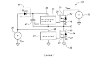
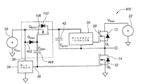
図1は、従来のハーフブリッジトポロジ10を示す。図示のように、従来のトポロジ10は、Q1及びQ2の符号が付された一対のトランジスタ12及び14を含む。そのようなトポロジは、例えば、エンハンスメント形電界効果トランジスタ(FETs)で実現されてもよい。典型的には、トランジスタ12及び14はハイサイド及びローサイドスイッチと見なされる。ハイサイドトランジスタ12のソース16は、ハーフブリッジの出力でローサイドトランジスタ14のドレイン18に結合されている。ハイサイドトランジスタ12のドレイン20は高電圧源22(VMain)に結合され、ローサイドトランジスタ14のソース24はグランド26に結合されている。さらに、ハイサイドトランジスタ12のゲート28は、ゲートドライバ・レベルシフタ30に結合されており、ローサイドトランジスタ14のゲート32はゲートドライバ34に結合される。ゲートドライバ・レベルシフタ30とゲートドライバ34とは、当技術分野で周知であり、ここでは詳細には説明しない。しかしながら、この構成は、動作中に1つのトランジスタ12又は14(Q1又はQ2)をスイッチオンし、他のトランジスタをスイッチオフすることを可能にし、逆も同様であることが理解されるべきである。
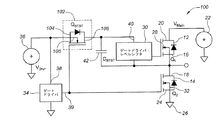
本発明は、ハーフブリッジトポロジのためのブートストラップサプライ(bootstrap supply)に関し、より詳細には、窒化ガリウム(GaN)FETを用いたブートストラップサプライに関する。有利には、GaN FETは、ゼロ逆回復電荷QRRを有し、ハーフブリッジ回路のローサイドトランジスタと同期してスイッチングすることができるので、高電圧アプリケーションに有用である。同期スイッチングは、FETのボディダイオードが導通した場合に、高ブートストラップサプライ電圧を阻止する。さらに、ブートストラップデバイスのゼロ逆回復電荷QRRは、スイッチング性能を、特に超低用量キャパシタデバイス対して著しく改善し、ハイサイドデバイス内への損失の誘発を低減する。
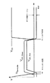
適切なオフ状態マージンの一例を図4に示す。
Claims (24)
- ハーフブリッジトポロジで配置された電気回路であって、
ハイサイドトランジスタと、
ローサイドトランジスタと、
前記ハイサイドトランジスタのゲートに電気的に結合されたゲートドライバ・レベルシフタと、
前記ローサイドトランジスタのゲートに電気的に結合されたゲートドライバと、
前記ゲートドライバ・レベルシフタと並列に電気的に結合されたキャパシタと、
前記ゲートドライバ・レベルシフタの入力と前記ゲートドライバの入力とに電気的に結合された電圧源と、
前記電圧源と前記キャパシタとの間に電気的に結合されたブートストラップデバイスと、を備え、
前記ブートストラップデバイスは、GaN電界効果トランジスタである、電気回路。 - 前記ブートストラップデバイスは、デプレション形トランジスタであり、前記デプレション形トランジスタのゲートは、前記ゲートドライバの出力に電気的に結合されている、請求項1に記載の電気回路。
- 前記デプレション形トランジスタは、前記ゲートドライバ・レベルシフタの前記入力に電気的に結合されている、請求項2に記載の電気回路。
- 前記ブートストラップデバイスは、前記ローサイドトランジスタに同期している、請求項1に記載の電気回路。
- 前記ブートストラップデバイスは、エンハンスメント形トランジスタである、請求項1に記載の電気回路。
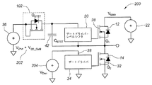
- 前記エンハンスメント形トランジスタはクランプされていない、請求項5に記載の電気回路。
- 前記エンハンスメント形トランジスタは、キャパシタと並列なツェナーダイオードでクランプされている、請求項5に記載の電気回路。
- 前記ゲートドライバに供給されるよりも高い電圧が、前記エンハンスメント形トランジスタに供給される、請求項5に記載の電気回路。
- さらに、前記ゲートドライバと電気的に通信するレギュレータを備える、請求項5に記載の電気回路。
- さらに、前記エンハンスメント形トランジスタのドレインと前記ツェナーダイオードとの間に直列に抵抗を備える、請求項7に記載の電気回路。
- 前記抵抗は、前記エンハンスメント形トランジスタ内に集積化されている、請求項10に記載の電気回路。
- 前記エンハンスメント形トランジスタは、それぞれのソースに短絡された各ゲートに直列に結合された、2つのエンハンスメント形GaN電界効果トランジスタでクランプされている、請求項5に記載の電気回路。
- さらに、前記のブートストラップデバイスであるトランジスタのゲートとソースとの間に電気的に結合されたダイオードと、
前記のブートストラップデバイスであるトランジスタのゲートと前記ゲートドライバの出力との間に結合された第2のキャパシタと、を備える、請求項1に記載の電気回路。 - 前記ブートストラップデバイスは、前記ハイサイドトランジスタ及び前記ローサイドトランジスタと集積化されている、請求項1に記載の電気回路。
- ハーフブリッジ回路をブートストラップする方法であって、
前記ハーフブリッジ回路のローサイドデバイスで、GaN電界効果トランジスタを同期してスイッチングするステップを含む、方法。 - 前記ローサイドデバイスは、トランジスタである、請求項15に記載の方法。
- 前記GaN電界効果トランジスタは、そのゲートが、前記ローサイドデバイスの前記ゲートと電気的に通信するゲートドライバの出力と電気的に通信する、請求項15に記載の方法。
- 前記GaN電界効果トランジスタのソースとドレインにわたる電圧は、前記ローサイドトランジスタのソースとドレインにわたる電圧に等しい、請求項16に記載の方法。
- 前記のローサイドデバイスであるトランジスタのゲートとソースにわたる電圧は、ゼロ(0)ボルトであり、前記GaN電界効果トランジスタのゲートとドレインにわたる電圧は、ドレイン電流の値が最低の場合に、マイナス5(−5)ボルトである、請求項18に記載の方法。
- 前記GaN電界効果トランジスタは、クランプされていないエンハンスメント形トランジスタであり、
追加電圧は前記GaN電界効果トランジスタに供給され、増加し、前記GaN電界効果トランジスタのボディダイオードにわたる電圧降下を克服する、請求項15に記載の方法。 - 前記GaN電界効果トランジスタはエンハンスメント形トランジスタであり、キャパシタ、ゲートドライバ・レベルシフタと並列なツェナーダイオードでクランプされ、前記ゲートドライバ・レベルシフタは、ハーフブリッジ回路のアッパーサイドデバイスと電気的に通信する、請求項15に記載の方法。
- 前記ツェナーダイオードは、前記キャパシタにわたる電圧を前記ローサイドデバイスの安全レベルにクランプする、請求項21に記載の方法。
- 前記エンハンスメント形トランジスタのドレインとツェナーダイオードの間に、抵抗が直列に結合されている、請求項21に記載の方法。
- ダイオードが、駆動電圧と前記GaN電界効果トランジスタのゲートとの間に電気的に結合されており、
キャパシタが、前記GaN電界効果トランジスタのゲートと前記ローサイドデバイスに対するゲートドライバの出力の間に電気的に結合されている、請求項15記載の方法。
Applications Claiming Priority (3)
| Application Number | Priority Date | Filing Date | Title |
|---|---|---|---|
| US201462062445P | 2014-10-10 | 2014-10-10 | |
| US62/062,445 | 2014-10-10 | ||
| PCT/US2015/054851 WO2016057878A1 (en) | 2014-10-10 | 2015-10-09 | High voltage zero qrr bootstrap supply |
Publications (3)
| Publication Number | Publication Date |
|---|---|
| JP2017537584A true JP2017537584A (ja) | 2017-12-14 |
| JP2017537584A5 JP2017537584A5 (ja) | 2018-11-15 |
| JP6703983B2 JP6703983B2 (ja) | 2020-06-03 |
Family
ID=55653829
Family Applications (1)
| Application Number | Title | Priority Date | Filing Date |
|---|---|---|---|
| JP2017519239A Expired - Fee Related JP6703983B2 (ja) | 2014-10-10 | 2015-10-09 | 高電圧ゼロqrrブートスタート電源 |
Country Status (7)
| Country | Link |
|---|---|
| US (2) | US9667245B2 (ja) |
| EP (1) | EP3205021B1 (ja) |
| JP (1) | JP6703983B2 (ja) |
| KR (1) | KR102458233B1 (ja) |
| CN (1) | CN107078736B (ja) |
| TW (1) | TWI607626B (ja) |
| WO (1) | WO2016057878A1 (ja) |
Cited By (2)
| Publication number | Priority date | Publication date | Assignee | Title |
|---|---|---|---|---|
| US11128295B1 (en) | 2020-03-19 | 2021-09-21 | Kabushiki Kaisha Toshiba | Semiconductor device |
| JP7550175B2 (ja) | 2020-01-14 | 2024-09-12 | ローム株式会社 | 半導体装置 |
Families Citing this family (34)
| Publication number | Priority date | Publication date | Assignee | Title |
|---|---|---|---|---|
| TWI566328B (zh) | 2013-07-29 | 2017-01-11 | 高效電源轉換公司 | 具有用於產生附加構件之多晶矽層的氮化鎵電晶體 |
| JP6378003B2 (ja) * | 2014-08-27 | 2018-08-22 | ラピスセミコンダクタ株式会社 | 半導体装置、電池監視システム、及び半導体装置の起動方法 |
| JP7080185B2 (ja) | 2016-05-25 | 2022-06-03 | エフィシエント パワー コンヴァーション コーポレーション | エンハンスメントモードfetドライバic |
| US10394260B2 (en) * | 2016-06-30 | 2019-08-27 | Synaptics Incorporated | Gate boosting circuit and method for an integrated power stage |
| JP6828296B2 (ja) * | 2016-08-09 | 2021-02-10 | 株式会社Gsユアサ | 蓄電装置および蓄電装置の充電制御方法 |
| DE112017006120B4 (de) | 2016-12-01 | 2020-12-10 | Efficient Power Conversion Corporation | Bootstrap-kondensator-überspannungs-überwachungsschaltung für wandler auf gan-transistorbasis |
| US10103629B2 (en) * | 2017-02-14 | 2018-10-16 | Nxp B.V. | High side driver without dedicated supply in high voltage applications |
| KR102498234B1 (ko) * | 2017-04-10 | 2023-02-09 | 마이크로칩 테크놀로지 인코포레이티드 | 하이-사이드 스위치를 위한 슬루 제어 |
| US10637456B2 (en) | 2017-07-20 | 2020-04-28 | Efficient Power Conversion Corporation | Low voltage drop cascaded synchronous bootstrap supply circuit |
| US10193554B1 (en) * | 2017-11-15 | 2019-01-29 | Navitas Semiconductor, Inc. | Capacitively coupled level shifter |
| US10778219B2 (en) | 2017-11-15 | 2020-09-15 | Navitas Semiconductor, Inc. | Level shifting in a GaN half bridge circuit |
| TWI663821B (zh) * | 2018-01-11 | 2019-06-21 | 晶豪科技股份有限公司 | 自舉式電路以及使用該自舉式電路之關聯的直流轉直流轉換器 |
| US11070203B2 (en) * | 2018-02-19 | 2021-07-20 | Cirrus Logic, Inc. | Dual bootstrapping for an open-loop pulse width modulation driver |
| CN108494234B (zh) * | 2018-04-09 | 2020-05-01 | 电子科技大学 | 适用于GaN高速栅驱动电路的浮动电源轨 |
| US10742121B2 (en) * | 2018-06-29 | 2020-08-11 | Dialog Semiconductor Inc. | Boot strap capacitor charging for switching power converters |
| EP3826164A4 (en) * | 2018-07-19 | 2021-07-14 | Mitsubishi Electric Corporation | POWER CONVERTER DEVICE, MOTOR DRIVE DEVICE AND AIR CONDITIONING SYSTEM |
| US10536070B1 (en) * | 2018-08-01 | 2020-01-14 | Infineon Technologies Ag | Driver for switching gallium nitride (GaN) devices |
| TWI732280B (zh) * | 2018-08-28 | 2021-07-01 | 美商高效電源轉換公司 | 串級自舉式GaN功率開關及驅動器 |
| US11303116B2 (en) * | 2018-08-29 | 2022-04-12 | Allegro Microsystems, Llc | Methods and apparatus for electrical overstress protection |
| US10574229B1 (en) | 2019-01-23 | 2020-02-25 | Tagore Technology, Inc. | System and device for high-side supply |
| US10601302B1 (en) * | 2019-04-04 | 2020-03-24 | Navitas Semiconductor, Inc. | Bootstrap power supply circuit |
| CN109995235B (zh) * | 2019-04-30 | 2024-03-08 | 广东美的制冷设备有限公司 | 智能功率模块和电器设备 |
| KR102230129B1 (ko) * | 2020-01-31 | 2021-03-22 | 청주대학교 산학협력단 | 부트스트랩 회로 및 이를 포함하는 전원 공급 장치 |
| IT202000016072A1 (it) * | 2020-07-02 | 2022-01-02 | St Microelectronics Srl | Circuito di pilotaggio, dispositivo e procedimento di funzionamento corrispondenti |
| CN216672983U (zh) | 2020-07-02 | 2022-06-03 | 意法半导体股份有限公司 | 电路及电子设备 |
| CN113054831B (zh) * | 2021-04-30 | 2022-03-29 | 杰华特微电子股份有限公司 | 一种三电平开关电路 |
| CN113746305B (zh) * | 2021-08-30 | 2023-04-25 | 深圳数马电子技术有限公司 | 栅极驱动电路和多相智能功率模块 |
| TWI778854B (zh) * | 2021-11-03 | 2022-09-21 | 新唐科技股份有限公司 | 電子系統及晶片 |
| WO2023107885A1 (en) * | 2021-12-08 | 2023-06-15 | Efficient Power Conversion Corporation | Active bootstrapping drivers |
| CN114421946B (zh) * | 2022-01-19 | 2024-07-02 | 科能芯(深圳)半导体有限公司 | 一种低反向导通压降的耗尽型功率器件的直驱电路 |
| TWI871686B (zh) | 2022-06-29 | 2025-02-01 | 美商高效電源轉換公司 | 通用功率場效電晶體(fet)驅動器積體電路(ic)架構 |
| US12381478B2 (en) * | 2023-05-23 | 2025-08-05 | Murata Manufacturing Co., Ltd. | Circuits and methods to startup and shutdown multi-level converters |
| CN117767711B (zh) * | 2024-02-22 | 2024-05-24 | 杰华特微电子股份有限公司 | 单向导通电路、桥式驱动电路及开关电源 |
| TWI901054B (zh) * | 2024-03-27 | 2025-10-11 | 晶炫半導體股份有限公司 | 邏輯閘電路 |
Citations (4)
| Publication number | Priority date | Publication date | Assignee | Title |
|---|---|---|---|---|
| JP2007318891A (ja) * | 2006-05-25 | 2007-12-06 | Toyota Industries Corp | スイッチング素子駆動用電源回路 |
| JP2011509629A (ja) * | 2008-01-11 | 2011-03-24 | インターナショナル レクティフィアー コーポレイション | 集積iii族窒化物電力変換回路 |
| JP2011188178A (ja) * | 2010-03-08 | 2011-09-22 | Sanken Electric Co Ltd | ゲートドライブ回路 |
| WO2013138750A1 (en) * | 2012-03-16 | 2013-09-19 | Texas Instruments Incorporated | SYSTEM AND APPARATUS FOR DRIVER CIRCUIT FOR PROTECTION OF GATES OF GaN FETS |
Family Cites Families (16)
| Publication number | Priority date | Publication date | Assignee | Title |
|---|---|---|---|---|
| US5182468A (en) * | 1989-02-13 | 1993-01-26 | Ibm Corporation | Current limiting clamp circuit |
| US5373435A (en) * | 1993-05-07 | 1994-12-13 | Philips Electronics North America Corporation | High voltage integrated circuit driver for half-bridge circuit employing a bootstrap diode emulator |
| JP3219019B2 (ja) * | 1997-05-30 | 2001-10-15 | 関西日本電気株式会社 | 異常電流検出回路およびそれを用いた負荷駆動回路 |
| US7456658B2 (en) | 2006-04-07 | 2008-11-25 | International Rectifier Corporation | Circuit to optimize charging of bootstrap capacitor with bootstrap diode emulator |
| TW200835125A (en) | 2007-02-08 | 2008-08-16 | Richtek Techohnology Corp | Circuit for charging the boot-strap capacitor of voltage converter |
| US20080290841A1 (en) | 2007-05-23 | 2008-11-27 | Richtek Technology Corporation | Charging Circuit for Bootstrap Capacitor and Integrated Driver Circuit Using Same |
| WO2009002541A1 (en) | 2007-06-27 | 2008-12-31 | International Rectifier Corporation | Gate driving scheme for depletion mode devices in buck converters |
| US8659275B2 (en) | 2008-01-11 | 2014-02-25 | International Rectifier Corporation | Highly efficient III-nitride power conversion circuit |
| US8154334B2 (en) | 2009-07-21 | 2012-04-10 | Intersil America Inc. | System and method for pre-charging a bootstrap capacitor in a switching regulator with high pre-bias voltage |
| JP5457826B2 (ja) * | 2009-12-28 | 2014-04-02 | 株式会社ジャパンディスプレイ | レベルシフト回路、信号駆動回路、表示装置および電子機器 |
| WO2012015427A1 (en) | 2010-07-30 | 2012-02-02 | Otis Elevator Company | Regulated bootstrap power supply |
| JP2013062717A (ja) * | 2011-09-14 | 2013-04-04 | Mitsubishi Electric Corp | 半導体装置 |
| JP5236822B1 (ja) | 2012-01-30 | 2013-07-17 | シャープ株式会社 | ドライバ回路 |
| US9209793B2 (en) * | 2012-02-17 | 2015-12-08 | Infineon Technologies Austria Ag | Bootstrap circuitry for an IGBT |
| CN103683872A (zh) * | 2012-09-11 | 2014-03-26 | 深圳市海洋王照明工程有限公司 | 一种半桥驱动电路 |
| US9171738B2 (en) * | 2012-12-18 | 2015-10-27 | Infineon Technologies Austria Ag | Systems and methods for integrating bootstrap circuit elements in power transistors and other devices |
-
2015
- 2015-10-07 US US14/877,613 patent/US9667245B2/en active Active
- 2015-10-08 TW TW104133258A patent/TWI607626B/zh active
- 2015-10-09 EP EP15848411.3A patent/EP3205021B1/en active Active
- 2015-10-09 KR KR1020177012061A patent/KR102458233B1/ko active Active
- 2015-10-09 WO PCT/US2015/054851 patent/WO2016057878A1/en not_active Ceased
- 2015-10-09 JP JP2017519239A patent/JP6703983B2/ja not_active Expired - Fee Related
- 2015-10-09 CN CN201580056930.1A patent/CN107078736B/zh active Active
-
2017
- 2017-04-26 US US15/497,637 patent/US10084445B2/en active Active
Patent Citations (4)
| Publication number | Priority date | Publication date | Assignee | Title |
|---|---|---|---|---|
| JP2007318891A (ja) * | 2006-05-25 | 2007-12-06 | Toyota Industries Corp | スイッチング素子駆動用電源回路 |
| JP2011509629A (ja) * | 2008-01-11 | 2011-03-24 | インターナショナル レクティフィアー コーポレイション | 集積iii族窒化物電力変換回路 |
| JP2011188178A (ja) * | 2010-03-08 | 2011-09-22 | Sanken Electric Co Ltd | ゲートドライブ回路 |
| WO2013138750A1 (en) * | 2012-03-16 | 2013-09-19 | Texas Instruments Incorporated | SYSTEM AND APPARATUS FOR DRIVER CIRCUIT FOR PROTECTION OF GATES OF GaN FETS |
Cited By (2)
| Publication number | Priority date | Publication date | Assignee | Title |
|---|---|---|---|---|
| JP7550175B2 (ja) | 2020-01-14 | 2024-09-12 | ローム株式会社 | 半導体装置 |
| US11128295B1 (en) | 2020-03-19 | 2021-09-21 | Kabushiki Kaisha Toshiba | Semiconductor device |
Also Published As
| Publication number | Publication date |
|---|---|
| JP6703983B2 (ja) | 2020-06-03 |
| WO2016057878A1 (en) | 2016-04-14 |
| TWI607626B (zh) | 2017-12-01 |
| US20170230046A1 (en) | 2017-08-10 |
| US10084445B2 (en) | 2018-09-25 |
| US20160105173A1 (en) | 2016-04-14 |
| KR102458233B1 (ko) | 2022-10-24 |
| US9667245B2 (en) | 2017-05-30 |
| CN107078736B (zh) | 2021-01-22 |
| EP3205021A1 (en) | 2017-08-16 |
| KR20170069244A (ko) | 2017-06-20 |
| EP3205021B1 (en) | 2021-12-01 |
| EP3205021A4 (en) | 2018-06-13 |
| CN107078736A (zh) | 2017-08-18 |
| TW201622348A (zh) | 2016-06-16 |
Similar Documents
| Publication | Publication Date | Title |
|---|---|---|
| JP6703983B2 (ja) | 高電圧ゼロqrrブートスタート電源 | |
| US8816666B2 (en) | Semiconductor switching device drive circuit using a limited drive voltage | |
| US9954522B2 (en) | Hybrid switch including GaN HEMT and MOSFET | |
| EP3590189B1 (en) | Hybrid switch control | |
| US9793260B2 (en) | System and method for a switch having a normally-on transistor and a normally-off transistor | |
| US9935551B2 (en) | Switching circuit including serially connected transistors for reducing transient current at time of turning off, and power supply circuit provided therewith | |
| CN104767360B (zh) | 用于驱动开关的系统和方法 | |
| US9515649B2 (en) | Cascode circuit | |
| US10686361B2 (en) | Synchronous rectifier gate driver with active clamp | |
| CN107979360B (zh) | 可配置电路及其操作方法和集成电路 | |
| JP2019537417A (ja) | GaNトランジスタに基づく電力コンバータのためのブートストラップキャパシタ過電圧管理回路 | |
| CN110299835B (zh) | 用于为开关转换器供电的系统和方法 | |
| JP5263317B2 (ja) | 半導体スイッチング素子の駆動回路 | |
| TW201607244A (zh) | 包含高功率增強模式的氮化鎵電晶體與驅動電路的電源切換系統 | |
| JPWO2014196136A1 (ja) | ゲートドライバおよびこれを備えたパワーモジュール | |
| JP6988256B2 (ja) | 電力変換器 | |
| CN102480216A (zh) | 用于驱动共源共栅开关的系统和方法 | |
| EP3070830B1 (en) | Rectifier circuit with reduced reverse recovery time | |
| HK1242058B (zh) | 高電壓零反向恢復電荷自舉供應器 | |
| HK1242058A1 (en) | High voltage zero qrr bootstrap supply | |
| CN117040516A (zh) | 基于半导体的晶体管的电压栅极驱动器、功率开关器件及相应方法 | |
| JP2015037226A (ja) | スイッチング素子用ゲート駆動回路 | |
| JP2017070198A (ja) | 電力変換装置 |
Legal Events
| Date | Code | Title | Description |
|---|---|---|---|
| A521 | Request for written amendment filed |
Free format text: JAPANESE INTERMEDIATE CODE: A523 Effective date: 20181005 |
|
| A621 | Written request for application examination |
Free format text: JAPANESE INTERMEDIATE CODE: A621 Effective date: 20181005 |
|
| A977 | Report on retrieval |
Free format text: JAPANESE INTERMEDIATE CODE: A971007 Effective date: 20190807 |
|
| A131 | Notification of reasons for refusal |
Free format text: JAPANESE INTERMEDIATE CODE: A131 Effective date: 20190813 |
|
| A521 | Request for written amendment filed |
Free format text: JAPANESE INTERMEDIATE CODE: A523 Effective date: 20191113 |
|
| A131 | Notification of reasons for refusal |
Free format text: JAPANESE INTERMEDIATE CODE: A131 Effective date: 20200212 |
|
| A521 | Request for written amendment filed |
Free format text: JAPANESE INTERMEDIATE CODE: A523 Effective date: 20200310 |
|
| TRDD | Decision of grant or rejection written | ||
| A01 | Written decision to grant a patent or to grant a registration (utility model) |
Free format text: JAPANESE INTERMEDIATE CODE: A01 Effective date: 20200414 |
|
| A61 | First payment of annual fees (during grant procedure) |
Free format text: JAPANESE INTERMEDIATE CODE: A61 Effective date: 20200511 |
|
| R150 | Certificate of patent or registration of utility model |
Ref document number: 6703983 Country of ref document: JP Free format text: JAPANESE INTERMEDIATE CODE: R150 |
|
| R250 | Receipt of annual fees |
Free format text: JAPANESE INTERMEDIATE CODE: R250 |
|
| R250 | Receipt of annual fees |
Free format text: JAPANESE INTERMEDIATE CODE: R250 |
|
| LAPS | Cancellation because of no payment of annual fees |