JP2017537584A - High voltage zero QRR boot start power supply - Google Patents
High voltage zero QRR boot start power supply Download PDFInfo
- Publication number
- JP2017537584A JP2017537584A JP2017519239A JP2017519239A JP2017537584A JP 2017537584 A JP2017537584 A JP 2017537584A JP 2017519239 A JP2017519239 A JP 2017519239A JP 2017519239 A JP2017519239 A JP 2017519239A JP 2017537584 A JP2017537584 A JP 2017537584A
- Authority
- JP
- Japan
- Prior art keywords
- transistor
- gate
- gate driver
- voltage
- bootstrap
- Prior art date
- Legal status (The legal status is an assumption and is not a legal conclusion. Google has not performed a legal analysis and makes no representation as to the accuracy of the status listed.)
- Granted
Links
Images

Classifications
-
- H—ELECTRICITY
- H03—ELECTRONIC CIRCUITRY
- H03K—PULSE TECHNIQUE
- H03K17/00—Electronic switching or gating, i.e. not by contact-making and –breaking
- H03K17/51—Electronic switching or gating, i.e. not by contact-making and –breaking characterised by the components used
- H03K17/56—Electronic switching or gating, i.e. not by contact-making and –breaking characterised by the components used by the use, as active elements, of semiconductor devices
- H03K17/567—Circuits characterised by the use of more than one type of semiconductor device, e.g. BIMOS, composite devices such as IGBT
-
- H—ELECTRICITY
- H03—ELECTRONIC CIRCUITRY
- H03K—PULSE TECHNIQUE
- H03K17/00—Electronic switching or gating, i.e. not by contact-making and –breaking
- H03K17/04—Modifications for accelerating switching
- H03K17/042—Modifications for accelerating switching by feedback from the output circuit to the control circuit
- H03K17/04206—Modifications for accelerating switching by feedback from the output circuit to the control circuit in field-effect transistor switches
-
- H—ELECTRICITY
- H03—ELECTRONIC CIRCUITRY
- H03K—PULSE TECHNIQUE
- H03K17/00—Electronic switching or gating, i.e. not by contact-making and –breaking
- H03K17/16—Modifications for eliminating interference voltages or currents
- H03K17/161—Modifications for eliminating interference voltages or currents in field-effect transistor switches
- H03K17/165—Modifications for eliminating interference voltages or currents in field-effect transistor switches by feedback from the output circuit to the control circuit
-
- H—ELECTRICITY
- H03—ELECTRONIC CIRCUITRY
- H03K—PULSE TECHNIQUE
- H03K17/00—Electronic switching or gating, i.e. not by contact-making and –breaking
- H03K17/51—Electronic switching or gating, i.e. not by contact-making and –breaking characterised by the components used
- H03K17/56—Electronic switching or gating, i.e. not by contact-making and –breaking characterised by the components used by the use, as active elements, of semiconductor devices
- H03K17/687—Electronic switching or gating, i.e. not by contact-making and –breaking characterised by the components used by the use, as active elements, of semiconductor devices the devices being field-effect transistors
- H03K17/6871—Electronic switching or gating, i.e. not by contact-making and –breaking characterised by the components used by the use, as active elements, of semiconductor devices the devices being field-effect transistors the output circuit comprising more than one controlled field-effect transistor
-
- H—ELECTRICITY
- H03—ELECTRONIC CIRCUITRY
- H03K—PULSE TECHNIQUE
- H03K19/00—Logic circuits, i.e. having at least two inputs acting on one output; Inverting circuits
- H03K19/0175—Coupling arrangements; Interface arrangements
- H03K19/017509—Interface arrangements
-
- H—ELECTRICITY
- H03—ELECTRONIC CIRCUITRY
- H03K—PULSE TECHNIQUE
- H03K2217/00—Indexing scheme related to electronic switching or gating, i.e. not by contact-making or -breaking covered by H03K17/00
- H03K2217/0063—High side switches, i.e. the higher potential [DC] or life wire [AC] being directly connected to the switch and not via the load
-
- H—ELECTRICITY
- H03—ELECTRONIC CIRCUITRY
- H03K—PULSE TECHNIQUE
- H03K2217/00—Indexing scheme related to electronic switching or gating, i.e. not by contact-making or -breaking covered by H03K17/00
- H03K2217/0072—Low side switches, i.e. the lower potential [DC] or neutral wire [AC] being directly connected to the switch and not via the load
-
- H—ELECTRICITY
- H03—ELECTRONIC CIRCUITRY
- H03K—PULSE TECHNIQUE
- H03K2217/00—Indexing scheme related to electronic switching or gating, i.e. not by contact-making or -breaking covered by H03K17/00
- H03K2217/0081—Power supply means, e.g. to the switch driver
Landscapes
- Engineering & Computer Science (AREA)
- Computer Hardware Design (AREA)
- Physics & Mathematics (AREA)
- Computing Systems (AREA)
- General Engineering & Computer Science (AREA)
- Mathematical Physics (AREA)
- Electronic Switches (AREA)
- Power Conversion In General (AREA)
- Dc-Dc Converters (AREA)
Abstract
ハーフブリッジトポロジに配置された電気回路である。電気回路は、ハイサイドトランジスタと、ローサイドトランジスタと、ハイサイドトランジスタのゲートに電気的に結合されたゲートドライバ・レベルシフタと、ローサイドトランジスタのゲートに電気的に結合されたゲートドライバと、ゲートドライバ・レベルシフタと並列に電気的に結合されたキャパシタと、ゲートドライバ・レベルシフタの入力とゲートドライバの入力とに電気的に結合された電圧源と、電圧源とキャパシタとの間に電気的に結合されたブートストラップトランジスタを有する。GaN電界効果トランジスタは、ハーフブリッジ回路のローサイドデバイス同期してスイッチングされる。An electrical circuit arranged in a half-bridge topology. The electrical circuit includes a high side transistor, a low side transistor, a gate driver level shifter electrically coupled to the gate of the high side transistor, a gate driver electrically coupled to the gate of the low side transistor, and a gate driver level shifter. A capacitor electrically coupled in parallel with the gate driver, a voltage source electrically coupled to the gate driver level shifter input and the gate driver input, and a boot electrically coupled between the voltage source and the capacitor. It has a strap transistor. The GaN field effect transistor is switched in synchronism with the low-side device of the half-bridge circuit.
Description
発明の背景
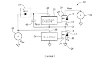
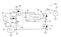
図1は、従来のハーフブリッジトポロジ10を示す。図示のように、従来のトポロジ10は、Q1及びQ2の符号が付された一対のトランジスタ12及び14を含む。そのようなトポロジは、例えば、エンハンスメント形電界効果トランジスタ(FETs)で実現されてもよい。典型的には、トランジスタ12及び14はハイサイド及びローサイドスイッチと見なされる。ハイサイドトランジスタ12のソース16は、ハーフブリッジの出力でローサイドトランジスタ14のドレイン18に結合されている。ハイサイドトランジスタ12のドレイン20は高電圧源22(VMain)に結合され、ローサイドトランジスタ14のソース24はグランド26に結合されている。さらに、ハイサイドトランジスタ12のゲート28は、ゲートドライバ・レベルシフタ30に結合されており、ローサイドトランジスタ14のゲート32はゲートドライバ34に結合される。ゲートドライバ・レベルシフタ30とゲートドライバ34とは、当技術分野で周知であり、ここでは詳細には説明しない。しかしながら、この構成は、動作中に1つのトランジスタ12又は14(Q1又はQ2)をスイッチオンし、他のトランジスタをスイッチオフすることを可能にし、逆も同様であることが理解されるべきである。
BACKGROUND OF THE INVENTION FIG. 1 shows a conventional half-
図1に示されるように、駆動電圧源36(VDrvr)は、ハイサイドゲートドライバ・レベルシフタ30の入力40と結合されており、かつ、ローサイドゲートドライバ34の入力38に結合されている。この従来の設計では、ブートストラップキャパシタ42(CBTST)は、ハイサイドゲートドライバ・レベルシフタ30と並列に結合され、ブートストラップダイオード44(DBTST)は、駆動電圧源36VDrvrとブートストラップキャパシタ42(CBTST)との間に結合される。ハイサイドトランジスタQ1及びローサイドトランジスタQ2に、eGaN FETを用いた場合、図1に示される構成は、ローサイドトランジスタが14(Q2)の「ボディダイオード」が導通する場合には、例えばブートストラップキャパシタ42(CBTST)にまたがって(across)、約7.5Vを生じる。しかしながら、電圧はいくつかの要因によって変わることがある。電圧は、動作条件及びローサイドトランジスタ14(Q2)に使用されるトランジスタデバイスのタイプに依存して、約6.5V以上にすることができる。しかしながら、この構成では、ハイサイドゲートドライバ30は何らかの形式のレギュレータを必要とする。従来、これはハーフブリッジ構成内のハイサイドトランジスタに電力を供給するために使用される内部ブートストラップダイオードで実現されている。理想的には、ショットキーダイオードが、小さく、順方向電圧降下が低く、逆回復電荷がないために使用される。しかしながら、集積回路プロセスにおいて高電圧(100V)ショットキーダイオードを作ることは非常に困難であり、従って、逆回復電荷を有するPN接合ダイオードがしばしば用いられる。さらに、高電圧ショットキーダイオードは、損失をもたらす逆回復電荷(QRR)を有する。
As shown in FIG. 1, the drive voltage source 36 (V Drvr ) is coupled to the
このために、このタイプのハーフブリッジトポロジのためにトランジスタ12及び14(Q1及びQ2)にGaN FETを使用すると、ショットキーダイオード又はPN接合ダイオードの逆回復電荷QRRが性能に影響を与え、ハイサイドトランジスタにおいて損失を誘発する。通常、これらの損失は、回路内の他の電力損失メカニズムと比較して無視できる程度である。しかしながら、逆回復電荷損失は周波数に比例し、より高い動作周波数ではコンバータ損失のかなりの部分になる点まで増加する。したがって、ブートストラップの従来の方法は、高いスイッチング周波数の動作では効率的ではない。
For this, the use of GaN
発明の概要
本発明は、ハーフブリッジトポロジのためのブートストラップサプライ(bootstrap supply)に関し、より詳細には、窒化ガリウム(GaN)FETを用いたブートストラップサプライに関する。有利には、GaN FETは、ゼロ逆回復電荷QRRを有し、ハーフブリッジ回路のローサイドトランジスタと同期してスイッチングすることができるので、高電圧アプリケーションに有用である。同期スイッチングは、FETのボディダイオードが導通した場合に、高ブートストラップサプライ電圧を阻止する。さらに、ブートストラップデバイスのゼロ逆回復電荷QRRは、スイッチング性能を、特に超低用量キャパシタデバイス対して著しく改善し、ハイサイドデバイス内への損失の誘発を低減する。
The present invention relates to a bootstrap supply for half-bridge topologies, and more particularly to a bootstrap supply using gallium nitride (GaN) FETs. Advantageously, GaN FETs are useful for high voltage applications because they have zero reverse recovery charge QRR and can be switched in synchronism with the low-side transistor of the half-bridge circuit. Synchronous switching prevents high bootstrap supply voltage when the FET's body diode conducts. Furthermore, the zero reverse recovery charge Q RR of the bootstrap device significantly improves switching performance, especially for ultra low dose capacitor devices, and reduces the induction of losses into the high side device.
このために、ハーフブリッジトポロジに配置された電気回路が提供される。電気回路は、ハイサイドトランジスタと、ローサイドトランジスタと、ハイサイドトランジスタのゲートに電気的に結合されたハイサイドゲートドライバ・レベルシフタと、ローサイドトランジスタのゲートに電気的に結合されたローサイドゲートドライバと、ハイサイドゲートドライバ・レベルシフタと並列に電気的に結合されたキャパシタと、ハイサイドゲートドライバ・レベルシフタの入力とローサイドゲートドライバの入力とに電気的に結合された電圧源と、電圧源とキャパシタの間に結合されたブートストラップトランジスタとを備える。 For this purpose, an electrical circuit arranged in a half-bridge topology is provided. The electrical circuit includes a high side transistor, a low side transistor, a high side gate driver level shifter electrically coupled to the gate of the high side transistor, a low side gate driver electrically coupled to the gate of the low side transistor, A capacitor electrically coupled in parallel with the side gate driver level shifter, a voltage source electrically coupled to the input of the high side gate driver level shifter and the input of the low side gate driver, and between the voltage source and the capacitor And a coupled bootstrap transistor.
いくつかの実施形態では、ブートストラップトランジスタはGaN電界効果トランジスタである。実施形態に応じて、ブートストラップトランジスタは、デプレッション形トランジスタ又はエンハンスメント形トランジスタであってもよい。ブートストラップトランジスタがデプレッション形トランジスタであるいくつかの実施形態では、デプレッション形トランジスタのゲートは、ゲートドライバの出力に電気的に結合される。デプレッション形の実施形態では、デプレッション形トランジスタのドレインは、ハイサイドゲートドライバ・レベルシフタの入力に電気的に結合される。 In some embodiments, the bootstrap transistor is a GaN field effect transistor. Depending on the embodiment, the bootstrap transistor may be a depletion type transistor or an enhancement type transistor. In some embodiments where the bootstrap transistor is a depletion type transistor, the gate of the depletion type transistor is electrically coupled to the output of the gate driver. In the depletion type embodiment, the drain of the depletion type transistor is electrically coupled to the input of the high side gate driver level shifter.
エンハンスメント形トランジスタがブートストラップデバイスとして使用される場合、実施形態に応じてクランプ(clamped)されてもクランプされていなくてもよい。エンハンスメント形トランジスタがクランプされている場合は、ブートストラップキャパシタと並列にツェナーダイオードでクランプすることができる。エンハンスメント形トランジスタのドレインとツェナーダイオードとの間に抵抗を直列に配置することができる。抵抗は、エンハンスメント形トランジスタに集積されてもよい。好ましくは、ツェナーダイオードは、ブートストラップキャパシタをまたぐ電圧をアッパーサイドデバイスに対する安全レベルにクランプする。 When an enhancement-type transistor is used as a bootstrap device, it may or may not be clamped depending on the embodiment. If the enhancement transistor is clamped, it can be clamped with a Zener diode in parallel with the bootstrap capacitor. A resistor can be placed in series between the drain of the enhancement transistor and the Zener diode. The resistor may be integrated into the enhancement type transistor. Preferably, the Zener diode clamps the voltage across the bootstrap capacitor to a safe level for the upper side device.
エンハンスメント形トランジスタは、それぞれのソースに短絡されたゲートと直列に結合された2つのエンハンスメント形GaN電界効果トランジスタでクランプされてもよい。 The enhancement type transistor may be clamped with two enhancement type GaN field effect transistors coupled in series with a gate shorted to the respective source.
エンハンスメント形トランジスタが使用される実施形態では、エンハンスメント形トランジスタに供給される電圧は、ゲートドライバに供給される電圧よりも高い電圧であり得る。これらの実施形態のいくつかでは、1つ以上の電圧源を使用することができる。 In embodiments where enhancement-type transistors are used, the voltage supplied to the enhancement-type transistor can be higher than the voltage supplied to the gate driver. In some of these embodiments, one or more voltage sources can be used.
いくつかの実施形態では、ローサイドゲートドライバを調整する必要がある場合がある。いくつかの実施形態では、レギュレータがローサイドゲートドライバとの電気的な通信内に配置されてもよい。 In some embodiments, the low side gate driver may need to be adjusted. In some embodiments, the regulator may be placed in electrical communication with the low side gate driver.
いくつかの実施形態では、ダイオードは、電源電圧とトランジスタのゲートとの間に電気的に結合され、第2のキャパシタは、トランジスタのゲートとゲートドライバの出力との間に電気的に結合される。 In some embodiments, the diode is electrically coupled between the power supply voltage and the gate of the transistor, and the second capacitor is electrically coupled between the gate of the transistor and the output of the gate driver. .
本発明の別の態様では、ハーフブリッジ回路をブートストラップする方法が提供される。好ましい実施形態では、GaN電界効果トランジスタは、ハーフブリッジ回路の、好ましくはGaN電界効果トランジスタであるローサイドトランジスタと同期してスイッチングされる。 In another aspect of the invention, a method for bootstrapping a half-bridge circuit is provided. In a preferred embodiment, the GaN field effect transistor is switched in synchronism with a low side transistor, preferably a GaN field effect transistor, of a half bridge circuit.
好ましい実施形態では、GaN電界効果トランジスタのソースとドレインにわたる電圧は、ローサイドデバイストランジスタのソースとドレインにわたる電圧に等しい。 In a preferred embodiment, the voltage across the source and drain of the GaN field effect transistor is equal to the voltage across the source and drain of the low side device transistor.
いくつかの実施形態では、ローサイドデバイストランジスタのゲートとソースにわたる電圧はゼロ(0)ボルトであり、ドレイン電流の値が最低(worst)の場合に、GaN電界効果トランジスタのゲートとソースにわたる電圧はマイナス5(−5)ボルトである。 In some embodiments, the voltage across the gate and source of the low-side device transistor is zero (0) volts, and the voltage across the gate and source of the GaN field effect transistor is negative when the drain current value is the worst. 5 (-5) bolts.
図面の簡単な説明
以下の詳細な説明では、本発明の例示的な実施形態を参照する。例示的な実施形態は、当業者がそれらを実施できるように十分詳細に記載されている。他の実施形態を採用してもよく、様々な構造的、論理的及び電気的な変更を行うことができることを理解されたい。 In the following detailed description, reference is made to exemplary embodiments of the invention. Exemplary embodiments are described in sufficient detail to enable those skilled in the art to practice them. It should be understood that other embodiments may be employed and that various structural, logical and electrical changes may be made.
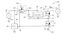
図2は、本発明の第1の実施形態100によるハーフブリッジトポロジのためのブートストラップサプライを示す。図示されているように、図2の設計は、上述した従来のハーフブリッジトポロジ10と同じ構成要素の多くを含む。すなわち、ハイサイドトランジスタ12及びローサイドトランジスタ14(Q1及び42)が設けられ、そのそれぞれのゲートは、それぞれ、ハイサイドゲートドライバ・レベルシフタ30へ、及び、ローサイドゲートドライバ34へ結合される。しかしながら、図1の従来の設計とは対照的に、図2の例示的な設計は、ブートストラップデバイス102として、デプレッション形トランジスタ(例えば、nチャンネルのデプレッション形電界効果トランジスタ(FET))が用いられている。好ましくは、ブートストラップデバイス102(QBTST)は、GaN FETである。
FIG. 2 shows a bootstrap supply for a half-bridge topology according to the
図示のように、ブートストラップデバイス102(QBTST)のソース104は、電圧源36(VDrvr)に結合される。ブートストラップデバイス102(QBTST)のゲート106は、ローサイドゲートドライバ34の出力39に結合される。ブートストラップデバイス102(QBTST)のドレイン108は、ハイサイドゲートドライバ・レベルシフタ30の入力40に結合される。有利には、例示的な実施形態のブートストラップデバイス102(QBTST)は、ローサイドトランジスタ14(Q2)のスイッチングに同期され、従来の設計について上述したブートストラップキャパシタ42(CsrsT)にわたる7.5Vを克服する(overcome)。
As shown, the
ブートストラップデバイス102(QBTST)のソースとドレインにわたる電圧VSDは、トランジスタ14(Q2)のソースとドレインにわたる電圧と同じであるべきである。さらに、トランジスタ14(Q2)のゲートとソースにわたる電圧VGS=0ボルトであり、ブートストラップデバイス102(QBTST)のゲートとソースにわたる電圧VGSは−5ボルトであり、ただし、ドレイン電流(ID)の値は最低の場合である。ドレインとソースの間の電圧VDSが、ブートストラップデバイス102(QBTST)とメイントランジスタ12及び/又は14(FETs Q1及び/又はQ2)の両方に対して同じ定格を有しているべきだが、ブートストラップデバイス102(QBTST)は著しく小さく(より高いRDS(on))できる。さらに、ブートストラップデバイス102(QBTST)は、集積化されたハーフブリッジデバイスペア内に集積化することができる。
The voltage V SD across the source and drain of the bootstrap device 102 (Q BTST ) should be the same as the voltage across the source and drain of the transistor 14 (Q2). Further, a voltage V GS = 0 volts across the gate and source of the transistor 14 (Q2), the voltage V GS across the gate and source of the bootstrap device 102 (Q BTST) is -5 volts, however, the drain current (ID ) Is the lowest value. The voltage V DS between the drain and source should have the same rating for both the bootstrap device 102 (Q BTST ) and the
同期FETの実装を保証するために、ブートストラップ回路10は、ゲートドライバへ及び電力回路への最小の影響を有し、いかなる条件においても動作し、回路10は厳しい条件下でロバストであるように設計されている必要がある。好ましい実施形態では、次の条件、すなわちローサイドFET逆導通(reverse conduction)、ローサイド逆導通(高損失COSS遷移)後のハードスイッチング、部分ゼロ電圧スイッチング(PZVS)、自己整流後のアッパーFETの逆導、及び、最も厳しくない条件のゼロ電圧スイッチング(ZVS)、によって説明されうる。
In order to ensure the implementation of the synchronous FET, the
上述したように、ブートストラップデバイス102にFETを使用する実施形態は、好ましくは同期される。図3は、FETブートストラップデバイス102を含むブートストラップ回路の好ましい実施形態のタイミングチャートを示す。正しいタイミングは、上に列挙した厳しい条件の影響を操作又は除去するのを助ける。動作中に、ローサイドトランジスタ14のゲート電圧の上昇に続いて、スイッチノード電圧がハイからローに遷移するのには時間がかかる。小同期FETブートストラップデバイス102が時期を早めてオンにされたとすると、ドレイン電圧はまだハイである。この条件では、スイッチノードは5Vに結合されており、破滅的な結果となる。したがって、この発生を避けるために、同期FETブートストラップデバイス102のターンオンは、十分に遅らされなければならない。この遅れは、VGS_Qlow及びVGS_BTSTの立ち上がりの差として、図3に示されている。同様の理由から、同期FETブートストラップデバイス102のターンオフは、ローサイドトランジスタ14と同時に行われなければならない。これも図3に示されている。
As mentioned above, embodiments using FETs for the
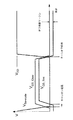
上に列挙した厳しい条件に耐える実施形態を設計するための別の重要な設計パラメータは、オフ状態マージンである。ローサイドトランジスタ14と同期FETブートストラップデバイス102の両方がeGaN FETデバイスであることができるので、両者は、オフ保持されているときに、同様の逆導通電圧降下を有しうる。これらの条件の下では、同期FETブートストラップデバイス102にとって、ローサイドトランジスタ14とともに又はローサイドトランジスタ14の代わりに主電流を逆転して導通させることが可能である。これは、ブートストラップキャパシタ42にわたる過電圧状態をもたらし、ハイサイドトランジスタのゲート28の故障をもたらす虞がある。この発生を防止するために、いくつかの実施形態では、同期FETブートストラップデバイス102のオフ状態電圧は−1Vに保持され、それにより、逆導通電圧が増加し、ローサイドトランジスタ14よりも著しく高くなり、従って導通を防止する。
適切なオフ状態マージンの一例を図4に示す。
Another important design parameter for designing an embodiment that can withstand the severe conditions listed above is the off-state margin. Since both the low-
An example of a suitable off-state margin is shown in FIG.
タイミング及びオフ状態マージンに加えて、好ましい実施形態は、ブートストラップデバイス102のドレイン回路がより高い電圧に共鳴するのを防止する回路レイアウトを使用する。同期FETブートストラップデバイス102のドレイン回路は、より高い電圧に共鳴する虞があり、これはブートストラップキャパシタ42を充電することができるより高い電圧にリングすることができ、ハイサイドトランジスタゲート28の故障をもたらす。
In addition to timing and off-state margins, the preferred embodiment uses a circuit layout that prevents the drain circuit of the
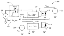
図4は、本発明の第2の実施形態200による、ハーフブリッジトポロジのためのブートストラップサプライを示す。図示されているように、図4の実施形態は、上述されたように、従来のハーフブリッジトポロジ10と同じ構成要素の多くを含む。すなわち、ハイサイドトランジスタ12及びローサイドトランジスタ14(Q1及びQ2)は、それぞれのゲート28及び32が、ゲートドライバ・レベルシフタ30とゲートドライバ34とにそれぞれ結合されている。しかしながら、図1の従来の設計10とは対照的に、ブートストラップデバイス102(QBTST)は、電圧源36(VDrvr)及びブートストラップキャパシタ42(CBTST)の間に結合された、クランプされていないエンハンスメント形デバイスである。さらに、追加の供給電圧202VSD_GaNが、ブートストラップデバイス102(QBTST)にも供給され、増加し、ブートストラップデバイスのGaN FETボディダイオードにわたる電圧降下を克服する。電圧源204(VDrvr)は、ローサイドゲートドライバ38に、追加の供給電圧202(VSD−GaN)なしで印加される。この構成は、トランジスタ14のボディダイオードが導通すると、ブートストラップキャパシタ42(CBTST)にわたる約7.5Vを生じる。しかしながら、ゲートドライバ34は、この構成に対して何らかの形式の調整を必要とする。実施形態に応じて、ゲートドライバ34は、内部的又は外部的に調整されてもよい。他の実施形態では、回路10のタイミングは、ローサイドゲートドライバ34を調整することができる。例えば、回路10を駆動する電圧源36を調整することができ、その調整は、回路が正常に動作するときに、順次ブートストラップキャパシタ42に伝えられることができる。図2の実施形態と同様に、ブートストラップデバイス102(QBTST)のソースとドレインにわたる電圧VSDは、トランジスタ14(Q2)のソースとドレインにわたる電圧と同一又は類似でなければならない。
FIG. 4 shows a bootstrap supply for a half-bridge topology according to the
図5の実施形態300は、図4の実施形態200の変形例を示す。基本的な違いは、ブートストラップ電源が、ブートストラップキャパシタ42(CBTST)に並列に結合されたツェナークランプ302(すなわち、ツェナーダイオードDCLMP)でクランプされることである。図5に示す実施形態300では、抵抗304RIlimは、ブートストラップデバイス102(QBTST)のドレイン108とツェナークランプDCLMPとの間に直列に結合されている。図5の構成は、トランジスタ14(Q2)のボディダイオードが導通した場合に、ブートストラップキャパシタ42(CBTST)にわたる電圧を安全な動作制限内に維持するために、ツェナークランプ302を用いる。さらに、ツェナークランプ302(DCLMP)は電圧をトランジスタ12(Q1)の安全制限にクランプし、抵抗304(RIlim)はクランプ中の電圧バッファを提供する。図2の実施形態100と同様に、ブートストラップデバイス102(QBTST)のソース及びドレインにわたる電圧VSDは、トランジスタ14(Q2)のソース及びドレインにわたる電圧と同一又は類似でなければならない。図4の構成200と同様に、ブートストラップデバイス102のボディダイオードにわたる電圧降下を克服するために、追加の供給電圧202(VSD_GaN)が、同様にブートストラップデバイス102に供給されている。
The
図5の例示的実施形態の一改良において、電流制御機能を備える抵抗304(RIlim)は、ブートストラップデバイス3102内に集積化されてもよい。いくつかの実施形態では、抵抗はRDS(on)すなわち、適切な抵抗を備えたFETの内部抵抗、を用いて集積化されてもよい。他の実施形態では、例えば金属バス(busing)などの抵抗素子を追加することができる。他の実施形態では、他の抵抗素子を使用することができる。抵抗素子304を集積することの利点の1つは、外部素子を除去することである。
In one refinement of the exemplary embodiment of FIG. 5, resistor 304 (R Ilim ) with current control functionality may be integrated within bootstrap device 3102. In some embodiments, the resistance may be integrated using RDS (on), the internal resistance of the FET with the appropriate resistance. In other embodiments, resistive elements, such as metal busing, can be added. In other embodiments, other resistive elements can be used. One advantage of integrating the
さらに他の実施形態では、ツェナークランプ302は、それぞれのソースに短絡されたゲートと直列に結合された2つのエンハンスメントGaNFETを使用することによって達成することができる。この設計は、回路設計のための最大の集積化を可能にしうる。
In yet another embodiment,
図6は、本開示の追加の実施形態400によるハーフブリッジトポロジのためのブートストラップサプライを示す。図示のように、図6の実施形態は、図2に示される実施形態100に関して上で説明されたハーフブリッジトポロジと同じ構成要素の多くを含む。例えば、実施形態400は、ハイサイドトランジスタ12とローサイドトランジスタ14と(Q1とQ2と)を含み、それぞれのゲート28とゲート32とがそれぞれゲートドライバ・レベルシフタ30とゲートドライバ34とに結合される。しかしながら、図2の設計とは対照的に、ブートストラップサプライは、同期エンハンスメント形デバイスの実装と見なすことができる。図示のように、ブートストラップデバイス102QBTSTは、駆動電圧源36(VDrvr)とハイサイドゲートドライバ・レベルシフタ30との間に結合されている。さらに、エンハンスメントダイオード402(DENH)が、駆動電圧源36(VDrvr)とブートストラップデバイス102(QBTST)のゲート106との間に結合されている。さらに、エンハンスメントキャパシタ404(CENH)がブートストラップデバイス102(QBTST)のゲート106と、ローゲートドライバ34の出力38との間に、結合されている。
FIG. 6 shows a bootstrap supply for a half-bridge topology according to an
いくつかの実施形態では、エンハンスメントダイオード402(DENH)は、外部コンポーネントの数を削減するためにブートストラップデバイス102に集積化されていてもよい。さらに他の実施形態では、エンハンスメントダイオード402と並列のエンハンスメント形抵抗もまた、ブートストラップデバイス102に集積化されていてもよい。
In some embodiments, enhancement diode 402 (D ENH ) may be integrated into
有利なことに、図5の実施形態のブートストラップデバイス102(QBTST)は、従来の設計では上述したようにブートストラップキャパシタ42(CBTST)にわたる7.5Vを克服するトランジスタ14(Q2)のスイッチングに同期している。同期することにより、ローサイドトランジスタ14の「ボディダイオード」が、ハイサイドトランジスタゲート28の過充電を防止する。例示的な実施形態では、ブートストラップデバイス102(QBTST)のソースとドレインにわたる電圧VSDは、トランジスタ14(Q2)のソースとドレインにわたる電圧と同じであるべきである。さらに、トランジスタ14(Q2)のソースとドレインにわたる電圧(VGS)=0ボルトであり、ブートストラップデバイス102(QBTST)のソースとドレインにわたる電圧(VGS)との間の電圧は、ドレイン電流IDの値が最低の場合に−5である。例示的な構成では、エンハンスメントダイオード402(DENH)の電圧降下は、ブートストラップデバイス102(QBTST)のゲートとソースにわたる電圧VGSを0Vよりも低下させ、したがってソースとドレインにわたる電圧VSDが上昇し、追加マージンのためのトランジスタ14(Q2)とブートストラップデバイス102(QBTST)との間の差異を増加させる。さらに、エンハンスメントキャパシタ404(CENH)は、従来のブートストラップサプライと同じ方法で(例えば、5Vに)充電される。しかしながら、使用されるエンハンスメントダイオード402(DENH)は、ゼロ又は超低逆回復電化量QRPを有する低電圧(例えば<20V)ショットキーダイオードであってもよい。
Advantageously, the bootstrap device 102 (Q BTST ) of the embodiment of FIG. 5 includes a transistor 14 (Q 2) that overcomes 7.5V across the bootstrap capacitor 42 (C BTST ) in the conventional design as described above. Synchronized with switching. By synchronizing, the “body diode” of the
上述の例示的な実施形態の各々について、ブートストラップデバイス102(QBTST)を駆動するための構成に、メイントランジスタ12及び14(Q1及びQ2)にスイッチング遷移、最も好ましくは、トランジスタ14(Q2)のターンオンイベントを完了するための時間を許すための、追加のタイミングを付けくわえることができると好ましい。さらに、ブートストラップデバイス102(QBTST)がオンになると、抵抗と同じように両方向に電流を伝導することができる。さらに、エンハンスメントキャパシタ(CENH)にわたる電圧は、オフ状態の間にブートストラップデバイス102(QBTST)の追加のボディダイオード電圧マージンを付け加えるために、制御され(低減され)ることができ、トランジスタ(Q2)の」ボディダイオードの導通の逆電圧が、ブートストラップサプライ電圧を安全動作制限を超えて増大させる可能性をさらに低減させる。
For each of the exemplary embodiments described above, the configuration for driving the bootstrap device 102 (Q BTST ) has a switching transition to the
いくつかの実施形態は、ブートストラップトランジスタ102がオンになる前にローサイドトランジスタ14が完全にオンになることを可能にするタイミング回路をさらに含むことができる。タイミング回路はまた、ローサイドトランジスタ14のゲートの電圧がゼロ(0)に低下したときに、ブートストラップトランジスタ102を直ちに、又はできるだけ早くオフにすることができる。
Some embodiments may further include a timing circuit that allows the
実験を通して、上述した実施形態は、抑制されていないと共鳴する虞があるブートストラップトランジスタ102のドレインインダクタンスに敏感であることが明らかになっている。トランジスタの設計/選択によって一般的にインダクタンス設計を維持する以外に、小さな直列抵抗がブートストラップトランジスタ102のドレインの後に直列に追加することができる。この抵抗を、ブートストラップトランジスタ102に集積化してもよい。いくつかの実施形態では、抵抗はブートストラップトランジスタ102の設計により、約3Ωの高RDS(on)と集積化されてもよい。さらに他の実施形態では、抵抗は、(RDS(on)ではなく別の)ただ集積された減衰抵抗であってもよい。
Through experimentation, it has been found that the above-described embodiments are sensitive to the drain inductance of the
図2、4乃至6に示す例示的な各実施形態のブートストラップデバイスに使用されるトランジスタは、好ましくは、GaN FETであると好ましい。最後に、上述したブートストラップデバイスの構成は、窒化ガリウム「GaN」FETを駆動するために提供されるが、例示的な実施形態には決して限定されず、(例えば、ハーフブリッジトポロジのための)通常のMOSFETを駆動するために使用されてもよい。さらに、上述した技術は、ハーフブリッジトランジスタもMOSFETであれば、ブートストラップデバイス102としてMOSFETを使用しても動作しない。これには2つの主な理由がある。1)適切に作動するために、ブートストラップトランジスタはGaNの逆導通電圧特性を利用しなければならず、電圧降下は負のゲート電圧の大きさによってプログラムされる。これは、内部ダイオードが導通しないようにしなければならないときに、内部ダイオードからの電磁波耐性を獲得する。MOSFETはこのように動作することができず、従って、主電源回路の一部となり、破壊的な結果を招く可能性がある。2)MOSFETはQrrを有するが、eGaN FETはQrrを有さない。(何らかの理由で)MOSFETダイオードが導通すると、ここで示した技術の利点は完全に失われる。
The transistors used in the bootstrap devices of the exemplary embodiments shown in FIGS. 2, 4 to 6 are preferably GaN FETs. Finally, the bootstrap device configuration described above is provided to drive gallium nitride “GaN” FETs, but is in no way limited to exemplary embodiments (eg, for half-bridge topologies). It may be used to drive a normal MOSFET. Further, the above-described technology does not operate even if a MOSFET is used as the
上記の説明及び図面は、本明細書に記載された特徴及び利点を達成する特定の実施形態を例示するものとしてだけ考慮されるべきである。特定のプロセス条件に対する変更及び置換を行うことができる。したがって、本発明の実施形態は、前述の説明及び図面によって限定されているとみなされない。 The above description and drawings should be considered merely as exemplifying specific embodiments that achieve the features and advantages described herein. Changes and substitutions can be made to specific process conditions. Accordingly, embodiments of the invention are not to be considered as limited by the foregoing description and drawings.
Claims (24)
ハイサイドトランジスタと、
ローサイドトランジスタと、
前記ハイサイドトランジスタのゲートに電気的に結合されたゲートドライバ・レベルシフタと、
前記ローサイドトランジスタのゲートに電気的に結合されたゲートドライバと、
前記ゲートドライバ・レベルシフタと並列に電気的に結合されたキャパシタと、
前記ゲートドライバ・レベルシフタの入力と前記ゲートドライバの入力とに電気的に結合された電圧源と、
前記電圧源と前記キャパシタとの間に電気的に結合されたブートストラップデバイスと、を備え、
前記ブートストラップデバイスは、GaN電界効果トランジスタである、電気回路。 An electrical circuit arranged in a half-bridge topology,
A high-side transistor,
A low-side transistor,
A gate driver level shifter electrically coupled to the gate of the high side transistor;
A gate driver electrically coupled to the gate of the low-side transistor;
A capacitor electrically coupled in parallel with the gate driver level shifter;
A voltage source electrically coupled to an input of the gate driver level shifter and an input of the gate driver;
A bootstrap device electrically coupled between the voltage source and the capacitor;
The bootstrap device is an electrical circuit, which is a GaN field effect transistor.
前記のブートストラップデバイスであるトランジスタのゲートと前記ゲートドライバの出力との間に結合された第2のキャパシタと、を備える、請求項1に記載の電気回路。 And a diode electrically coupled between the gate and source of the bootstrap device transistor;
The electrical circuit of claim 1, comprising a second capacitor coupled between a gate of a transistor that is the bootstrap device and an output of the gate driver.
前記ハーフブリッジ回路のローサイドデバイスで、GaN電界効果トランジスタを同期してスイッチングするステップを含む、方法。 A method of bootstrapping a half-bridge circuit,
Switching the GaN field-effect transistor synchronously at the low-side device of the half-bridge circuit.
追加電圧は前記GaN電界効果トランジスタに供給され、増加し、前記GaN電界効果トランジスタのボディダイオードにわたる電圧降下を克服する、請求項15に記載の方法。 The GaN field effect transistor is an unclamped enhancement type transistor,
The method of claim 15, wherein an additional voltage is provided to the GaN field effect transistor and increases to overcome a voltage drop across a body diode of the GaN field effect transistor.
キャパシタが、前記GaN電界効果トランジスタのゲートと前記ローサイドデバイスに対するゲートドライバの出力の間に電気的に結合されている、請求項15記載の方法。 A diode is electrically coupled between the drive voltage and the gate of the GaN field effect transistor;
The method of claim 15, wherein a capacitor is electrically coupled between a gate of the GaN field effect transistor and an output of a gate driver for the low side device.
Applications Claiming Priority (3)
| Application Number | Priority Date | Filing Date | Title |
|---|---|---|---|
| US201462062445P | 2014-10-10 | 2014-10-10 | |
| US62/062,445 | 2014-10-10 | ||
| PCT/US2015/054851 WO2016057878A1 (en) | 2014-10-10 | 2015-10-09 | High voltage zero qrr bootstrap supply |
Publications (3)
| Publication Number | Publication Date |
|---|---|
| JP2017537584A true JP2017537584A (en) | 2017-12-14 |
| JP2017537584A5 JP2017537584A5 (en) | 2018-11-15 |
| JP6703983B2 JP6703983B2 (en) | 2020-06-03 |
Family
ID=55653829
Family Applications (1)
| Application Number | Title | Priority Date | Filing Date |
|---|---|---|---|
| JP2017519239A Expired - Fee Related JP6703983B2 (en) | 2014-10-10 | 2015-10-09 | High voltage zero QRR boot start power supply |
Country Status (7)
| Country | Link |
|---|---|
| US (2) | US9667245B2 (en) |
| EP (1) | EP3205021B1 (en) |
| JP (1) | JP6703983B2 (en) |
| KR (1) | KR102458233B1 (en) |
| CN (1) | CN107078736B (en) |
| TW (1) | TWI607626B (en) |
| WO (1) | WO2016057878A1 (en) |
Cited By (2)
| Publication number | Priority date | Publication date | Assignee | Title |
|---|---|---|---|---|
| US11128295B1 (en) | 2020-03-19 | 2021-09-21 | Kabushiki Kaisha Toshiba | Semiconductor device |
| JP7550175B2 (en) | 2020-01-14 | 2024-09-12 | ローム株式会社 | Semiconductor Device |
Families Citing this family (34)
| Publication number | Priority date | Publication date | Assignee | Title |
|---|---|---|---|---|
| TWI566328B (en) | 2013-07-29 | 2017-01-11 | 高效電源轉換公司 | Gallium nitride transistor having a polysilicon layer for generating additional components |
| JP6378003B2 (en) * | 2014-08-27 | 2018-08-22 | ラピスセミコンダクタ株式会社 | Semiconductor device, battery monitoring system, and semiconductor device startup method |
| JP7080185B2 (en) | 2016-05-25 | 2022-06-03 | エフィシエント パワー コンヴァーション コーポレーション | Enhancement Mode FET Driver IC |
| US10394260B2 (en) * | 2016-06-30 | 2019-08-27 | Synaptics Incorporated | Gate boosting circuit and method for an integrated power stage |
| JP6828296B2 (en) * | 2016-08-09 | 2021-02-10 | 株式会社Gsユアサ | Power storage device and charge control method for power storage device |
| DE112017006120B4 (en) | 2016-12-01 | 2020-12-10 | Efficient Power Conversion Corporation | BOOTSTRAP CAPACITOR OVERVOLTAGE MONITORING CIRCUIT FOR CONVERTERS BASED ON GAN TRANSISTORS |
| US10103629B2 (en) * | 2017-02-14 | 2018-10-16 | Nxp B.V. | High side driver without dedicated supply in high voltage applications |
| KR102498234B1 (en) * | 2017-04-10 | 2023-02-09 | 마이크로칩 테크놀로지 인코포레이티드 | Slew Control for High-Side Switches |
| US10637456B2 (en) | 2017-07-20 | 2020-04-28 | Efficient Power Conversion Corporation | Low voltage drop cascaded synchronous bootstrap supply circuit |
| US10193554B1 (en) * | 2017-11-15 | 2019-01-29 | Navitas Semiconductor, Inc. | Capacitively coupled level shifter |
| US10778219B2 (en) | 2017-11-15 | 2020-09-15 | Navitas Semiconductor, Inc. | Level shifting in a GaN half bridge circuit |
| TWI663821B (en) * | 2018-01-11 | 2019-06-21 | 晶豪科技股份有限公司 | Bootstrap circuit and associated direct current-to-direct current converter applying the bootstrap circuit |
| US11070203B2 (en) * | 2018-02-19 | 2021-07-20 | Cirrus Logic, Inc. | Dual bootstrapping for an open-loop pulse width modulation driver |
| CN108494234B (en) * | 2018-04-09 | 2020-05-01 | 电子科技大学 | Floating power rail suitable for GaN high-speed gate drive circuit |
| US10742121B2 (en) * | 2018-06-29 | 2020-08-11 | Dialog Semiconductor Inc. | Boot strap capacitor charging for switching power converters |
| EP3826164A4 (en) * | 2018-07-19 | 2021-07-14 | Mitsubishi Electric Corporation | POWER CONVERSION UNIT, MOTOR DRIVE UNIT AND AIR CONDITIONER |
| US10536070B1 (en) * | 2018-08-01 | 2020-01-14 | Infineon Technologies Ag | Driver for switching gallium nitride (GaN) devices |
| TWI732280B (en) * | 2018-08-28 | 2021-07-01 | 美商高效電源轉換公司 | CASCADED BOOTSTRAPPING GaN POWER SWITCH AND DRIVER |
| US11303116B2 (en) * | 2018-08-29 | 2022-04-12 | Allegro Microsystems, Llc | Methods and apparatus for electrical overstress protection |
| US10574229B1 (en) | 2019-01-23 | 2020-02-25 | Tagore Technology, Inc. | System and device for high-side supply |
| US10601302B1 (en) * | 2019-04-04 | 2020-03-24 | Navitas Semiconductor, Inc. | Bootstrap power supply circuit |
| CN109995235B (en) * | 2019-04-30 | 2024-03-08 | 广东美的制冷设备有限公司 | Intelligent power module and electrical equipment |
| KR102230129B1 (en) * | 2020-01-31 | 2021-03-22 | 청주대학교 산학협력단 | Bootstrap circuit and power supply apparatus including the same |
| IT202000016072A1 (en) * | 2020-07-02 | 2022-01-02 | St Microelectronics Srl | CORRESPONDING DRIVE CIRCUIT, DEVICE AND OPERATING PROCEDURE |
| CN216672983U (en) | 2020-07-02 | 2022-06-03 | 意法半导体股份有限公司 | Circuits and Electronic Equipment |
| CN113054831B (en) * | 2021-04-30 | 2022-03-29 | 杰华特微电子股份有限公司 | A three-level switch circuit |
| CN113746305B (en) * | 2021-08-30 | 2023-04-25 | 深圳数马电子技术有限公司 | Gate driving circuit and multiphase intelligent power module |
| TWI778854B (en) * | 2021-11-03 | 2022-09-21 | 新唐科技股份有限公司 | Electronic system and chip |
| WO2023107885A1 (en) * | 2021-12-08 | 2023-06-15 | Efficient Power Conversion Corporation | Active bootstrapping drivers |
| CN114421946B (en) * | 2022-01-19 | 2024-07-02 | 科能芯(深圳)半导体有限公司 | Direct drive circuit of depletion type power device with low reverse conduction voltage drop |
| TWI871686B (en) | 2022-06-29 | 2025-02-01 | 美商高效電源轉換公司 | Universal power fet driver ic architecture |
| US12381478B2 (en) * | 2023-05-23 | 2025-08-05 | Murata Manufacturing Co., Ltd. | Circuits and methods to startup and shutdown multi-level converters |
| CN117767711B (en) * | 2024-02-22 | 2024-05-24 | 杰华特微电子股份有限公司 | One-way conduction circuit, bridge drive circuit and switching power supply |
| TWI901054B (en) * | 2024-03-27 | 2025-10-11 | 晶炫半導體股份有限公司 | Logic gate circuit |
Citations (4)
| Publication number | Priority date | Publication date | Assignee | Title |
|---|---|---|---|---|
| JP2007318891A (en) * | 2006-05-25 | 2007-12-06 | Toyota Industries Corp | Power circuit for driving switching element |
| JP2011509629A (en) * | 2008-01-11 | 2011-03-24 | インターナショナル レクティフィアー コーポレイション | Integrated III-nitride power conversion circuit |
| JP2011188178A (en) * | 2010-03-08 | 2011-09-22 | Sanken Electric Co Ltd | Gate drive circuit |
| WO2013138750A1 (en) * | 2012-03-16 | 2013-09-19 | Texas Instruments Incorporated | SYSTEM AND APPARATUS FOR DRIVER CIRCUIT FOR PROTECTION OF GATES OF GaN FETS |
Family Cites Families (16)
| Publication number | Priority date | Publication date | Assignee | Title |
|---|---|---|---|---|
| US5182468A (en) * | 1989-02-13 | 1993-01-26 | Ibm Corporation | Current limiting clamp circuit |
| US5373435A (en) * | 1993-05-07 | 1994-12-13 | Philips Electronics North America Corporation | High voltage integrated circuit driver for half-bridge circuit employing a bootstrap diode emulator |
| JP3219019B2 (en) * | 1997-05-30 | 2001-10-15 | 関西日本電気株式会社 | Abnormal current detection circuit and load drive circuit using the same |
| US7456658B2 (en) | 2006-04-07 | 2008-11-25 | International Rectifier Corporation | Circuit to optimize charging of bootstrap capacitor with bootstrap diode emulator |
| TW200835125A (en) | 2007-02-08 | 2008-08-16 | Richtek Techohnology Corp | Circuit for charging the boot-strap capacitor of voltage converter |
| US20080290841A1 (en) | 2007-05-23 | 2008-11-27 | Richtek Technology Corporation | Charging Circuit for Bootstrap Capacitor and Integrated Driver Circuit Using Same |
| WO2009002541A1 (en) | 2007-06-27 | 2008-12-31 | International Rectifier Corporation | Gate driving scheme for depletion mode devices in buck converters |
| US8659275B2 (en) | 2008-01-11 | 2014-02-25 | International Rectifier Corporation | Highly efficient III-nitride power conversion circuit |
| US8154334B2 (en) | 2009-07-21 | 2012-04-10 | Intersil America Inc. | System and method for pre-charging a bootstrap capacitor in a switching regulator with high pre-bias voltage |
| JP5457826B2 (en) * | 2009-12-28 | 2014-04-02 | 株式会社ジャパンディスプレイ | Level shift circuit, signal drive circuit, display device, and electronic device |
| WO2012015427A1 (en) | 2010-07-30 | 2012-02-02 | Otis Elevator Company | Regulated bootstrap power supply |
| JP2013062717A (en) * | 2011-09-14 | 2013-04-04 | Mitsubishi Electric Corp | Semiconductor device |
| JP5236822B1 (en) | 2012-01-30 | 2013-07-17 | シャープ株式会社 | Driver circuit |
| US9209793B2 (en) * | 2012-02-17 | 2015-12-08 | Infineon Technologies Austria Ag | Bootstrap circuitry for an IGBT |
| CN103683872A (en) * | 2012-09-11 | 2014-03-26 | 深圳市海洋王照明工程有限公司 | Half-bridge driving circuit |
| US9171738B2 (en) * | 2012-12-18 | 2015-10-27 | Infineon Technologies Austria Ag | Systems and methods for integrating bootstrap circuit elements in power transistors and other devices |
-
2015
- 2015-10-07 US US14/877,613 patent/US9667245B2/en active Active
- 2015-10-08 TW TW104133258A patent/TWI607626B/en active
- 2015-10-09 EP EP15848411.3A patent/EP3205021B1/en active Active
- 2015-10-09 KR KR1020177012061A patent/KR102458233B1/en active Active
- 2015-10-09 WO PCT/US2015/054851 patent/WO2016057878A1/en not_active Ceased
- 2015-10-09 JP JP2017519239A patent/JP6703983B2/en not_active Expired - Fee Related
- 2015-10-09 CN CN201580056930.1A patent/CN107078736B/en active Active
-
2017
- 2017-04-26 US US15/497,637 patent/US10084445B2/en active Active
Patent Citations (4)
| Publication number | Priority date | Publication date | Assignee | Title |
|---|---|---|---|---|
| JP2007318891A (en) * | 2006-05-25 | 2007-12-06 | Toyota Industries Corp | Power circuit for driving switching element |
| JP2011509629A (en) * | 2008-01-11 | 2011-03-24 | インターナショナル レクティフィアー コーポレイション | Integrated III-nitride power conversion circuit |
| JP2011188178A (en) * | 2010-03-08 | 2011-09-22 | Sanken Electric Co Ltd | Gate drive circuit |
| WO2013138750A1 (en) * | 2012-03-16 | 2013-09-19 | Texas Instruments Incorporated | SYSTEM AND APPARATUS FOR DRIVER CIRCUIT FOR PROTECTION OF GATES OF GaN FETS |
Cited By (2)
| Publication number | Priority date | Publication date | Assignee | Title |
|---|---|---|---|---|
| JP7550175B2 (en) | 2020-01-14 | 2024-09-12 | ローム株式会社 | Semiconductor Device |
| US11128295B1 (en) | 2020-03-19 | 2021-09-21 | Kabushiki Kaisha Toshiba | Semiconductor device |
Also Published As
| Publication number | Publication date |
|---|---|
| JP6703983B2 (en) | 2020-06-03 |
| WO2016057878A1 (en) | 2016-04-14 |
| TWI607626B (en) | 2017-12-01 |
| US20170230046A1 (en) | 2017-08-10 |
| US10084445B2 (en) | 2018-09-25 |
| US20160105173A1 (en) | 2016-04-14 |
| KR102458233B1 (en) | 2022-10-24 |
| US9667245B2 (en) | 2017-05-30 |
| CN107078736B (en) | 2021-01-22 |
| EP3205021A1 (en) | 2017-08-16 |
| KR20170069244A (en) | 2017-06-20 |
| EP3205021B1 (en) | 2021-12-01 |
| EP3205021A4 (en) | 2018-06-13 |
| CN107078736A (en) | 2017-08-18 |
| TW201622348A (en) | 2016-06-16 |
Similar Documents
| Publication | Publication Date | Title |
|---|---|---|
| JP6703983B2 (en) | High voltage zero QRR boot start power supply | |
| US8816666B2 (en) | Semiconductor switching device drive circuit using a limited drive voltage | |
| US9954522B2 (en) | Hybrid switch including GaN HEMT and MOSFET | |
| EP3590189B1 (en) | Hybrid switch control | |
| US9793260B2 (en) | System and method for a switch having a normally-on transistor and a normally-off transistor | |
| US9935551B2 (en) | Switching circuit including serially connected transistors for reducing transient current at time of turning off, and power supply circuit provided therewith | |
| CN104767360B (en) | System and method for driving switch | |
| US9515649B2 (en) | Cascode circuit | |
| US10686361B2 (en) | Synchronous rectifier gate driver with active clamp | |
| CN107979360B (en) | Configurable circuit, operation method thereof and integrated circuit | |
| JP2019537417A (en) | Bootstrap capacitor overvoltage management circuit for power converter based on GaN transistor | |
| CN110299835B (en) | System and method for powering a switching converter | |
| JP5263317B2 (en) | Semiconductor switching element drive circuit | |
| TW201607244A (en) | Power switching system for gallium nitride transistor and driving circuit including high power enhancement mode | |
| JPWO2014196136A1 (en) | Gate driver and power module including the same | |
| JP6988256B2 (en) | Power converter | |
| CN102480216A (en) | System and method for driving acascode switch | |
| EP3070830B1 (en) | Rectifier circuit with reduced reverse recovery time | |
| HK1242058B (en) | High voltage zero qrr bootstrap supply | |
| HK1242058A1 (en) | High voltage zero qrr bootstrap supply | |
| CN117040516A (en) | Voltage gate driver, power switching device and corresponding methods for semiconductor-based transistors | |
| JP2015037226A (en) | Gate drive circuit for switching element | |
| JP2017070198A (en) | Power converter |
Legal Events
| Date | Code | Title | Description |
|---|---|---|---|
| A521 | Request for written amendment filed |
Free format text: JAPANESE INTERMEDIATE CODE: A523 Effective date: 20181005 |
|
| A621 | Written request for application examination |
Free format text: JAPANESE INTERMEDIATE CODE: A621 Effective date: 20181005 |
|
| A977 | Report on retrieval |
Free format text: JAPANESE INTERMEDIATE CODE: A971007 Effective date: 20190807 |
|
| A131 | Notification of reasons for refusal |
Free format text: JAPANESE INTERMEDIATE CODE: A131 Effective date: 20190813 |
|
| A521 | Request for written amendment filed |
Free format text: JAPANESE INTERMEDIATE CODE: A523 Effective date: 20191113 |
|
| A131 | Notification of reasons for refusal |
Free format text: JAPANESE INTERMEDIATE CODE: A131 Effective date: 20200212 |
|
| A521 | Request for written amendment filed |
Free format text: JAPANESE INTERMEDIATE CODE: A523 Effective date: 20200310 |
|
| TRDD | Decision of grant or rejection written | ||
| A01 | Written decision to grant a patent or to grant a registration (utility model) |
Free format text: JAPANESE INTERMEDIATE CODE: A01 Effective date: 20200414 |
|
| A61 | First payment of annual fees (during grant procedure) |
Free format text: JAPANESE INTERMEDIATE CODE: A61 Effective date: 20200511 |
|
| R150 | Certificate of patent or registration of utility model |
Ref document number: 6703983 Country of ref document: JP Free format text: JAPANESE INTERMEDIATE CODE: R150 |
|
| R250 | Receipt of annual fees |
Free format text: JAPANESE INTERMEDIATE CODE: R250 |
|
| R250 | Receipt of annual fees |
Free format text: JAPANESE INTERMEDIATE CODE: R250 |
|
| LAPS | Cancellation because of no payment of annual fees |