JP2016158366A - 半導体装置及びその制御方法 - Google Patents
半導体装置及びその制御方法 Download PDFInfo
- Publication number
- JP2016158366A JP2016158366A JP2015033926A JP2015033926A JP2016158366A JP 2016158366 A JP2016158366 A JP 2016158366A JP 2015033926 A JP2015033926 A JP 2015033926A JP 2015033926 A JP2015033926 A JP 2015033926A JP 2016158366 A JP2016158366 A JP 2016158366A
- Authority
- JP
- Japan
- Prior art keywords
- control
- signal
- proportional
- control signal
- voltage
- Prior art date
- Legal status (The legal status is an assumption and is not a legal conclusion. Google has not performed a legal analysis and makes no representation as to the accuracy of the status listed.)
- Granted
Links
Images


Classifications
-
- H—ELECTRICITY
- H02—GENERATION; CONVERSION OR DISTRIBUTION OF ELECTRIC POWER
- H02M—APPARATUS FOR CONVERSION BETWEEN AC AND AC, BETWEEN AC AND DC, OR BETWEEN DC AND DC, AND FOR USE WITH MAINS OR SIMILAR POWER SUPPLY SYSTEMS; CONVERSION OF DC OR AC INPUT POWER INTO SURGE OUTPUT POWER; CONTROL OR REGULATION THEREOF
- H02M3/00—Conversion of DC power input into DC power output
- H02M3/02—Conversion of DC power input into DC power output without intermediate conversion into AC
- H02M3/04—Conversion of DC power input into DC power output without intermediate conversion into AC by static converters
- H02M3/10—Conversion of DC power input into DC power output without intermediate conversion into AC by static converters using discharge tubes with control electrode or semiconductor devices with control electrode
- H02M3/145—Conversion of DC power input into DC power output without intermediate conversion into AC by static converters using discharge tubes with control electrode or semiconductor devices with control electrode using devices of a triode or transistor type requiring continuous application of a control signal
- H02M3/155—Conversion of DC power input into DC power output without intermediate conversion into AC by static converters using discharge tubes with control electrode or semiconductor devices with control electrode using devices of a triode or transistor type requiring continuous application of a control signal using semiconductor devices only
- H02M3/156—Conversion of DC power input into DC power output without intermediate conversion into AC by static converters using discharge tubes with control electrode or semiconductor devices with control electrode using devices of a triode or transistor type requiring continuous application of a control signal using semiconductor devices only with automatic control of output voltage or current, e.g. switching regulators
- H02M3/158—Conversion of DC power input into DC power output without intermediate conversion into AC by static converters using discharge tubes with control electrode or semiconductor devices with control electrode using devices of a triode or transistor type requiring continuous application of a control signal using semiconductor devices only with automatic control of output voltage or current, e.g. switching regulators including plural semiconductor devices as final control devices for a single load
- H02M3/1582—Buck-boost converters
-
- H—ELECTRICITY
- H02—GENERATION; CONVERSION OR DISTRIBUTION OF ELECTRIC POWER
- H02M—APPARATUS FOR CONVERSION BETWEEN AC AND AC, BETWEEN AC AND DC, OR BETWEEN DC AND DC, AND FOR USE WITH MAINS OR SIMILAR POWER SUPPLY SYSTEMS; CONVERSION OF DC OR AC INPUT POWER INTO SURGE OUTPUT POWER; CONTROL OR REGULATION THEREOF
- H02M1/00—Details of apparatus for conversion
- H02M1/0003—Details of control, feedback or regulation circuits
- H02M1/0025—Arrangements for modifying reference values, feedback values or error values in the control loop of a converter
Landscapes
- Engineering & Computer Science (AREA)
- Power Engineering (AREA)
- Dc-Dc Converters (AREA)
Abstract
【解決手段】一実施の形態によれば、DCDCコンバータ1は、インダクタL1及びスイッチ部を有し、パルス信号P1のデューティ比に応じた電圧分だけ入力電圧Vinを変化させた出力電圧Voutを生成する電源部12と、出力電圧Voutを分圧した電圧Vfbと、目標電圧Vcnstと、の差分である差分信号eに応じた制御信号Sを出力するPID制御器111と、制御信号Sと、インダクタL1に流れる平均電流を示す電流信号と、の差分である差分信号eiに応じた制御信号Dを出力するPI制御器112と、制御信号Dに応じたデューティ比のパルス信号P1を生成するPWM生成部113と、を備え、降圧時、PI制御器112は、制御信号D及び基準比例定数KPの乗算結果を比例定数として用いて差分信号eiの比例制御を行う。
【選択図】図1
Description
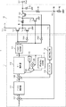
図1は、実施の形態1に係るDCDCコンバータ(半導体装置)1の構成を示す図である。DCDCコンバータ1は、例えば車両に搭載され、車載アナログ製品に対して安定した電圧を供給するために用いられる。
電源部12は、制御部11から供給されるパルス信号P1,P2のデューティ比に応じた電圧分だけ、入力電圧Vinを昇圧又は降圧した出力電圧Voutを生成する部である。
以下、電源部12の基本動作について簡単に説明する。
制御部11は、電源部12の昇圧又は降圧のレベルを制御するためのパルス信号P1,P2を出力する部である。
積分制御:KI×∫e(t)dt ・・・(2)
微分制御:KD×de(t)dt ・・・(3)
(降圧時):KP×D×ei(t) ・・・(4)
積分制御:KI×∫ei(t)dt ・・・(5)
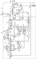
図2は、実施の形態2に係るDCDCコンバータ2の構成を示す図である。
図2に示すように、DCDCコンバータ2は、デジタル制御方式のDCDCコンバータであって、制御部11に代えて制御部21を備える。
図3は、実施の形態3に係るDCDCコンバータ3の構成を示す図である。
図3に示すように、DCDCコンバータ3は、デジタル制御方式のDCDCコンバータであって、制御部21に代えて制御部31を備える。
図4は、実施の形態4に係るDCDCコンバータ4の構成の一部を示す図である。
DCDCコンバータ4は、アナログ制御方式のDCDCコンバータである。
11,21,31 制御部
12 電源部
111,211,311 PID制御器
112,212 PI制御器
113,213 PWM生成部
114,214 電流検出部
115,215 フィルタ
116,216 昇圧降圧判定部
117,118 減算器
119,219 記憶部
120,220 乗算器
121,221 選択回路
217,218 減算器
222 フリップフロップ
223,224 ADコンバータ
225,226 乗算器
227 加算器
228 記憶部
229 フリップフロップ
230 加算器
331 利得部
332 選択回路
333 乗算器
334 積分器
335 微分器
336 加算器
412 PI制御器
413 アンプ
414 可変抵抗素子
415 容量素子
416 バッファ
417 リミッタ
C1 容量素子
INV1,INV2 インバータ
L1 インダクタ
R1,R2 抵抗素子
Tr1〜Tr4 トランジスタ
Claims (10)
- インダクタと、パルス信号によりオンオフが制御されることで当該インダクタに流れる電流を制御するスイッチ部と、を有し、前記パルス信号のデューティ比に応じた電圧分だけ入力電圧を変化させた出力電圧を生成する電源部と、
前記出力電圧に対応する比較電圧と、目標電圧と、の差分である第1差分信号のPI制御を行って第1制御信号を出力する第1制御部と、
前記第1制御信号と、前記インダクタに流れる電流の平均値を示す電流信号と、の差分である第2差分信号のPI制御を行って第2制御信号を出力する第2制御部と、
前記第2制御信号に応じたデューティ比の前記パルス信号を生成するPWM生成部と、を備え、
降圧時、前記第2制御部は、前記第2制御信号と基準比例定数との乗算結果を比例定数として用いて前記第2差分信号の比例制御を行う、半導体装置。 - 昇圧時、前記第2制御部は、前記基準比例定数を比例定数として用いて前記第2差分信号の比例制御を行う、請求項1に記載の半導体装置。
- 降圧時か昇圧時かを判定する判定回路と、
前記判定回路の判定結果に基づいて前記乗算結果及び前記基準比例定数の何れかを選択して出力する第1選択回路と、をさらに備え、
前記第2制御部は、前記第1選択回路の出力結果を比例定数として用いて前記第2差分信号の比例制御を行う、請求項2に記載の半導体装置。 - 前記第2制御部は、前記第1選択回路の出力結果を比例定数として用いて前記第2差分信号の比例制御を行うとともに、前記第2差分信号の積分制御を行って、前記第2制御信号を出力するPI制御器である、請求項3に記載の半導体装置。
- 前記第2制御部は、降圧時に前記乗算結果を比例定数として用いて前記第2差分信号の比例制御を行うとともに、前記第2差分信号の積分制御を行って、前記第2制御信号を出力するPI制御器である、請求項1に記載の半導体装置。
- 前記判定回路の判定結果に基づいて、前記基準比例定数と、前記基準比例定数を所定利得で増幅した定数と、の何れかを選択して出力する第2選択回路をさらに備え、
前記第1制御部は、前記第2選択回路の出力結果を比例定数として用いて前記第1差分信号の比例制御を行う、請求項3に記載の半導体装置。 - 前記第2制御部は、
アナログの前記第2制御信号と、アナログの前記電流信号と、の電位差を増幅して前記第2制御信号を出力するアンプと、
前記アンプの出力端子と接地電圧端子との間に設けられた容量素子と、
前記アンプの出力端子と前記容量素子との間に設けられ、前記第2制御信号に応じて抵抗値が変化する可変抵抗素子と、を有する、請求項1に記載の半導体装置。 - パルス信号によりインダクタに流れる電流を制御することで、当該パルス信号のデューティ比に応じた電圧分だけ入力電圧を変化させた出力電圧を生成する半導体装置の制御方法であって、
前記出力電圧に対応する比較電圧と、目標電圧と、の差分である第1差分信号のPI制御を行って第1制御信号を出力し、
降圧時、第2制御信号及び基準比例定数の乗算結果を比例定数として用いて、前記第1制御信号と、前記インダクタに流れる電流の平均値を示す電流信号と、の差分である第2差分信号の比例制御を行うとともに、当該第2差分信号の積分制御を行って、前記第2制御信号を出力し、
前記第2制御信号に応じたデューティ比の前記パルス信号を生成する、半導体装置の制御方法。 - 昇圧時、前記基準比例定数を比例定数として用いて前記第2差分信号の比例制御を行うとともに、当該第2差分信号の積分制御を行って、前記第2制御信号を出力する、請求項8に記載の半導体装置の制御方法。
- 降圧時か昇圧時かを判定し、
その判定結果に基づいて前記乗算結果及び前記基準比例定数の何れかを選択し、
選択された一方を比例定数として用いて前記第2差分信号の比例制御を行う、請求項9に記載の半導体装置の制御方法。
Priority Applications (3)
| Application Number | Priority Date | Filing Date | Title |
|---|---|---|---|
| JP2015033926A JP6445348B2 (ja) | 2015-02-24 | 2015-02-24 | 半導体装置及びその制御方法 |
| US14/991,399 US9654006B2 (en) | 2015-02-24 | 2016-01-08 | Semiconductor device and control method thereof |
| US15/490,248 US20170222558A1 (en) | 2015-02-24 | 2017-04-18 | Semiconductor device and control method thereof |
Applications Claiming Priority (1)
| Application Number | Priority Date | Filing Date | Title |
|---|---|---|---|
| JP2015033926A JP6445348B2 (ja) | 2015-02-24 | 2015-02-24 | 半導体装置及びその制御方法 |
Publications (2)
| Publication Number | Publication Date |
|---|---|
| JP2016158366A true JP2016158366A (ja) | 2016-09-01 |
| JP6445348B2 JP6445348B2 (ja) | 2018-12-26 |
Family
ID=56693848
Family Applications (1)
| Application Number | Title | Priority Date | Filing Date |
|---|---|---|---|
| JP2015033926A Active JP6445348B2 (ja) | 2015-02-24 | 2015-02-24 | 半導体装置及びその制御方法 |
Country Status (2)
| Country | Link |
|---|---|
| US (2) | US9654006B2 (ja) |
| JP (1) | JP6445348B2 (ja) |
Cited By (1)
| Publication number | Priority date | Publication date | Assignee | Title |
|---|---|---|---|---|
| WO2023129410A1 (en) * | 2021-12-28 | 2023-07-06 | Texas Instruments Incorporated | Voltage converter with average input current control and input-to-output isolation |
Families Citing this family (11)
| Publication number | Priority date | Publication date | Assignee | Title |
|---|---|---|---|---|
| JP6445348B2 (ja) * | 2015-02-24 | 2018-12-26 | ルネサスエレクトロニクス株式会社 | 半導体装置及びその制御方法 |
| US9979281B2 (en) * | 2016-10-07 | 2018-05-22 | Excelitas Technologies Corp. | Apparatus and method for dynamic adjustment of the bandwidth of a power converter |
| KR102510906B1 (ko) * | 2016-11-16 | 2023-03-15 | 삼성전자주식회사 | 반도체 장치 및 시스템 |
| CN107342675A (zh) * | 2017-06-26 | 2017-11-10 | 北京无线电测量研究所 | 一种数字电源控制方法、装置及系统 |
| CN111344939B (zh) * | 2017-11-24 | 2024-01-30 | 三菱电机株式会社 | 并联电源装置 |
| CN108761331A (zh) * | 2018-03-29 | 2018-11-06 | 广州视源电子科技股份有限公司 | 一种伺服系统的测试装置及测试方法 |
| JP7056393B2 (ja) * | 2018-06-14 | 2022-04-19 | トヨタ自動車株式会社 | 電圧変換器 |
| JP7385383B2 (ja) | 2019-06-21 | 2023-11-22 | ルネサスエレクトロニクス株式会社 | 半導体装置、システムおよび制御方法 |
| IT201900014715A1 (it) | 2019-08-13 | 2021-02-13 | St Microelectronics Srl | Dispositivo di controllo per regolatore di tensione a commutazione e metodo di controllo |
| EP3920397A1 (de) | 2020-06-03 | 2021-12-08 | Siemens Aktiengesellschaft | Verfahren zur regelung eines gleichspannungswandler |
| CN112415887B (zh) * | 2020-11-19 | 2022-06-21 | 合肥工业大学 | 计及功率损耗的全象限变流器的电压环控制方法及系统 |
Citations (5)
| Publication number | Priority date | Publication date | Assignee | Title |
|---|---|---|---|---|
| JP2005318743A (ja) * | 2004-04-28 | 2005-11-10 | Fuji Electric Systems Co Ltd | 直流昇圧回路の制御方法 |
| US20100131219A1 (en) * | 2008-11-21 | 2010-05-27 | Stewart Kenly | Digital compensator for power supply applications |
| US7804282B2 (en) * | 2006-11-21 | 2010-09-28 | Dialog Semiconductor Gmbh | Buck converter with inductor pre-energizing |
| JP2013197098A (ja) * | 2012-03-21 | 2013-09-30 | Dongwoon Anatech Co Ltd | 照明駆動装置及びその方法 |
| US20150214827A1 (en) * | 2014-01-28 | 2015-07-30 | Samsung Electronics Co., Ltd. | Voltage converter and power management device including the same |
Family Cites Families (3)
| Publication number | Priority date | Publication date | Assignee | Title |
|---|---|---|---|---|
| US7554473B2 (en) * | 2007-05-02 | 2009-06-30 | Cirrus Logic, Inc. | Control system using a nonlinear delta-sigma modulator with nonlinear process modeling |
| US9678521B2 (en) * | 2013-04-15 | 2017-06-13 | Virginia Tech Intellectual Properties, Inc. | External ramp autotuning for current mode control of switching converter |
| JP6445348B2 (ja) * | 2015-02-24 | 2018-12-26 | ルネサスエレクトロニクス株式会社 | 半導体装置及びその制御方法 |
-
2015
- 2015-02-24 JP JP2015033926A patent/JP6445348B2/ja active Active
-
2016
- 2016-01-08 US US14/991,399 patent/US9654006B2/en not_active Expired - Fee Related
-
2017
- 2017-04-18 US US15/490,248 patent/US20170222558A1/en not_active Abandoned
Patent Citations (5)
| Publication number | Priority date | Publication date | Assignee | Title |
|---|---|---|---|---|
| JP2005318743A (ja) * | 2004-04-28 | 2005-11-10 | Fuji Electric Systems Co Ltd | 直流昇圧回路の制御方法 |
| US7804282B2 (en) * | 2006-11-21 | 2010-09-28 | Dialog Semiconductor Gmbh | Buck converter with inductor pre-energizing |
| US20100131219A1 (en) * | 2008-11-21 | 2010-05-27 | Stewart Kenly | Digital compensator for power supply applications |
| JP2013197098A (ja) * | 2012-03-21 | 2013-09-30 | Dongwoon Anatech Co Ltd | 照明駆動装置及びその方法 |
| US20150214827A1 (en) * | 2014-01-28 | 2015-07-30 | Samsung Electronics Co., Ltd. | Voltage converter and power management device including the same |
Cited By (3)
| Publication number | Priority date | Publication date | Assignee | Title |
|---|---|---|---|---|
| WO2023129410A1 (en) * | 2021-12-28 | 2023-07-06 | Texas Instruments Incorporated | Voltage converter with average input current control and input-to-output isolation |
| US11881770B2 (en) | 2021-12-28 | 2024-01-23 | Texas Instruments Incorporated | Voltage converter with average input current control and input-to-output isolation |
| US12206326B2 (en) | 2021-12-28 | 2025-01-21 | Texas Instruments Incorporated | Voltage converter with average input current control and input-to-output isolation |
Also Published As
| Publication number | Publication date |
|---|---|
| US20160248325A1 (en) | 2016-08-25 |
| US9654006B2 (en) | 2017-05-16 |
| US20170222558A1 (en) | 2017-08-03 |
| JP6445348B2 (ja) | 2018-12-26 |
Similar Documents
| Publication | Publication Date | Title |
|---|---|---|
| JP6445348B2 (ja) | 半導体装置及びその制御方法 | |
| JP5901635B2 (ja) | ブリッジトポロジーを用いるスイッチドモード電力コンバータ及びそのスイッチング方法 | |
| JP5014772B2 (ja) | 電流モード制御型スイッチングレギュレータ | |
| JP4725641B2 (ja) | 昇降圧型スイッチングレギュレータ | |
| JP2017175746A (ja) | 電流検出回路及びそれを備えたdcdcコンバータ | |
| JP2007209103A (ja) | 電流モード制御dc−dcコンバータ | |
| JP2009033883A (ja) | スイッチングレギュレータ及びその動作制御方法 | |
| JP5865028B2 (ja) | Dcーdcコンバータ | |
| JP2010011576A (ja) | スイッチングレギュレータ | |
| JP2014050308A (ja) | スイッチングレギュレータとその制御方法 | |
| JP5855418B2 (ja) | スイッチングレギュレータ | |
| JP6203688B2 (ja) | 電源回路とその制御方法 | |
| JP6601211B2 (ja) | Dc−dcコンバータおよび負荷駆動用半導体集積回路 | |
| JP2015146711A (ja) | マルチフェーズ型dc/dcコンバータ | |
| Daraz et al. | Performance analysis of PID controller and fuzzy logic controller for DC-DC boost converter | |
| JP2006033958A (ja) | スイッチングレギュレータ | |
| JP5091101B2 (ja) | ソフトスタート回路及びそのソフトスタート回路を備えた電源回路 | |
| JP6160188B2 (ja) | スイッチングレギュレータ | |
| JPWO2011048796A1 (ja) | Dc−dcコンバータ | |
| KR20060049915A (ko) | Dc-dc 컨버터 회로 | |
| Chamundeeswari et al. | Design and Implementation of Fuzzy sliding mode control (FSMC) approach for a Modified Negative Output Luo DC-DC Converter with its comparative analysis | |
| JP6993867B2 (ja) | スイッチングレギュレータ及びその制御装置 | |
| JP2005218157A (ja) | Dc/dcコンバータ及びdc/dcコンバータの制御方法 | |
| CN103929059A (zh) | 转换器的电流限流方案 | |
| Karimi et al. | An improved integrated control modeling of a high-power density interleaved non-inverting buck-boost DC-DC converter |
Legal Events
| Date | Code | Title | Description |
|---|---|---|---|
| A621 | Written request for application examination |
Free format text: JAPANESE INTERMEDIATE CODE: A621 Effective date: 20171127 |
|
| A131 | Notification of reasons for refusal |
Free format text: JAPANESE INTERMEDIATE CODE: A131 Effective date: 20180828 |
|
| A977 | Report on retrieval |
Free format text: JAPANESE INTERMEDIATE CODE: A971007 Effective date: 20180831 |
|
| A521 | Request for written amendment filed |
Free format text: JAPANESE INTERMEDIATE CODE: A523 Effective date: 20181022 |
|
| TRDD | Decision of grant or rejection written | ||
| A01 | Written decision to grant a patent or to grant a registration (utility model) |
Free format text: JAPANESE INTERMEDIATE CODE: A01 Effective date: 20181127 |
|
| A61 | First payment of annual fees (during grant procedure) |
Free format text: JAPANESE INTERMEDIATE CODE: A61 Effective date: 20181129 |
|
| R150 | Certificate of patent or registration of utility model |
Ref document number: 6445348 Country of ref document: JP Free format text: JAPANESE INTERMEDIATE CODE: R150 |
|
| R250 | Receipt of annual fees |
Free format text: JAPANESE INTERMEDIATE CODE: R250 |