JP2016146403A - レーザー加工装置 - Google Patents
レーザー加工装置 Download PDFInfo
- Publication number
- JP2016146403A JP2016146403A JP2015022451A JP2015022451A JP2016146403A JP 2016146403 A JP2016146403 A JP 2016146403A JP 2015022451 A JP2015022451 A JP 2015022451A JP 2015022451 A JP2015022451 A JP 2015022451A JP 2016146403 A JP2016146403 A JP 2016146403A
- Authority
- JP
- Japan
- Prior art keywords
- wafer
- line
- laser beam
- chuck table
- virtual line
- Prior art date
- Legal status (The legal status is an assumption and is not a legal conclusion. Google has not performed a legal analysis and makes no representation as to the accuracy of the status listed.)
- Pending
Links
- 238000003754 machining Methods 0.000 title claims abstract description 5
- 238000003384 imaging method Methods 0.000 claims abstract description 20
- 238000012545 processing Methods 0.000 claims description 38
- 230000001678 irradiating effect Effects 0.000 claims description 9
- 238000006243 chemical reaction Methods 0.000 claims description 5
- 235000012431 wafers Nutrition 0.000 description 94
- 238000010586 diagram Methods 0.000 description 10
- 238000000034 method Methods 0.000 description 9
- 238000013461 design Methods 0.000 description 8
- 238000003860 storage Methods 0.000 description 5
- 230000001681 protective effect Effects 0.000 description 4
- 239000004065 semiconductor Substances 0.000 description 3
- 239000000758 substrate Substances 0.000 description 3
- 238000002679 ablation Methods 0.000 description 2
- 239000000919 ceramic Substances 0.000 description 2
- 238000005520 cutting process Methods 0.000 description 2
- 239000000463 material Substances 0.000 description 2
- 230000003287 optical effect Effects 0.000 description 2
- 239000000853 adhesive Substances 0.000 description 1
- 230000001070 adhesive effect Effects 0.000 description 1
- 230000015556 catabolic process Effects 0.000 description 1
- 238000012790 confirmation Methods 0.000 description 1
- 239000000470 constituent Substances 0.000 description 1
- 239000011521 glass Substances 0.000 description 1
- 229910010272 inorganic material Inorganic materials 0.000 description 1
- 239000011147 inorganic material Substances 0.000 description 1
- 238000004519 manufacturing process Methods 0.000 description 1
- 239000000155 melt Substances 0.000 description 1
- 238000012986 modification Methods 0.000 description 1
- 230000004048 modification Effects 0.000 description 1
- 238000003672 processing method Methods 0.000 description 1
- 239000011347 resin Substances 0.000 description 1
- 229920005989 resin Polymers 0.000 description 1
- 238000010079 rubber tapping Methods 0.000 description 1
- 230000011218 segmentation Effects 0.000 description 1
- 238000006467 substitution reaction Methods 0.000 description 1
- 238000012360 testing method Methods 0.000 description 1
Images


Abstract
Description
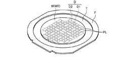
実施形態に係るレーザー加工装置1の構成例について説明する。図1は、レーザー加工装置の構成例を示す斜視図である。図2は、ウェーハの構成例を示す斜視図である。レーザー加工装置1は、レーザー光線をウェーハWの分割予定ラインPLに照射してウェーハWを加工するものである。レーザー加工装置1は、本体10と、チャックテーブル20と、レーザー光線照射手段30と、撮像手段40と、X軸移動手段50と、Y軸移動手段60と、タッチパネル70と、制御手段80とを備えている。
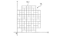
ウェーハW内部に改質層を形成するステルスダイシング加工に本発明を適用したが、これに限定されない。例えば、ウェーハWに加工溝を形成するアブレーション加工に本発明を適用してもよい。アブレーション加工においては、分割予定ラインPLに沿って形成する加工溝の始点と終点を示すX、Y座標情報をタッチパネル70から入力する。座標情報変換手段82は、加工溝の始点と終点を示すX、Y座標情報に基づいて加工溝が形成される位置を示す仮想線VLの情報を生成する。制御手段80は、ウェーハWの撮像画像と仮想線VLとを重ねてタッチパネル70に表示する。レーザー光線照射手段30は、X、Y座標情報に基づいてレーザー光線を分割予定ラインPLに沿って照射し、ウェーハWに加工溝を形成する。
20 チャックテーブル
30 レーザー光線照射手段
40 撮像手段
50 X軸移動手段
60 Y軸移動手段
70 タッチパネル
D デバイス
F 環状フレーム
KP キーパターン
P 起点
PL 分割予定ライン
T 保護テープ
VL 仮想線
W ウェーハ
WR 裏面
Claims (1)
- 互いに間隔を持って配列する複数のデバイス領域が表面に設定されたウェーハにおいて該間隔を分割予定ラインとし、レーザー光線を該分割予定ラインに照射して該ウェーハを加工するレーザー加工装置であって、
ウェーハを保持するチャックテーブルと、
該チャックテーブルに保持されたウェーハに該レーザー光線を照射するレーザー光線照射手段と、
該チャックテーブルと該レーザー光線照射手段とを加工送り方向であるX軸方向及び割り出し送り方向であるY軸方向に相対移動させる移動手段と、
該チャックテーブルに保持されたウェーハを撮像する撮像手段と、
該撮像手段で撮像した画像を表示する表示手段と、
ウェーハの表面に設定されたキーパターンを撮像し、該チャックテーブルに保持されたウェーハのX、Y座標の起点を割り出す起点算出手段と、
該分割予定ラインに照射する該レーザー光線の始点と終点のX、Y座標情報を入力する入力手段と、
該始点と該終点の該X、Y座標情報に基づいて該レーザー光線が照射される予定の位置を仮想線として表示する仮想線情報を生成する座標情報変換手段と、を備え、
該チャックテーブルに保持されたウェーハを該表示手段で表示する際に、ウェーハの画像と該仮想線とを重ねて表示させ、該仮想線と該分割予定ラインとの位置関係を画像で確認することを特徴とするレーザー加工装置。
Priority Applications (1)
| Application Number | Priority Date | Filing Date | Title |
|---|---|---|---|
| JP2015022451A JP2016146403A (ja) | 2015-02-06 | 2015-02-06 | レーザー加工装置 |
Applications Claiming Priority (1)
| Application Number | Priority Date | Filing Date | Title |
|---|---|---|---|
| JP2015022451A JP2016146403A (ja) | 2015-02-06 | 2015-02-06 | レーザー加工装置 |
Publications (1)
| Publication Number | Publication Date |
|---|---|
| JP2016146403A true JP2016146403A (ja) | 2016-08-12 |
Family
ID=56686511
Family Applications (1)
| Application Number | Title | Priority Date | Filing Date |
|---|---|---|---|
| JP2015022451A Pending JP2016146403A (ja) | 2015-02-06 | 2015-02-06 | レーザー加工装置 |
Country Status (1)
| Country | Link |
|---|---|
| JP (1) | JP2016146403A (ja) |
Cited By (4)
| Publication number | Priority date | Publication date | Assignee | Title |
|---|---|---|---|---|
| JP2020136555A (ja) * | 2019-02-22 | 2020-08-31 | 株式会社ディスコ | 加工装置 |
| JP2021044504A (ja) * | 2019-09-13 | 2021-03-18 | 株式会社ディスコ | 加工装置 |
| CN113310758A (zh) * | 2020-02-07 | 2021-08-27 | 台湾积体电路制造股份有限公司 | 显微试片制备方法、装置及记录介质 |
| DE102022210511A1 (de) | 2021-10-12 | 2023-04-13 | Disco Corporation | Bearbeitungsvorrichtung |
Citations (8)
| Publication number | Priority date | Publication date | Assignee | Title |
|---|---|---|---|---|
| JPS63101089A (ja) * | 1986-10-17 | 1988-05-06 | Mitsubishi Electric Corp | レ−ザ加工機制御装置 |
| US4896206A (en) * | 1987-12-14 | 1990-01-23 | Electro Science Industries, Inc. | Video detection system |
| JPH06232254A (ja) * | 1993-02-01 | 1994-08-19 | Sumitomo Electric Ind Ltd | 半導体ウェーハの切断ライン位置検出方法及び装置 |
| JP2009076484A (ja) * | 2007-09-18 | 2009-04-09 | Fujitsu Microelectronics Ltd | レーザダイシング装置及びダイシング方法 |
| JP2012148302A (ja) * | 2011-01-18 | 2012-08-09 | Olympus Corp | 調整装置、レーザ加工装置および調整方法 |
| JP2014070910A (ja) * | 2012-09-27 | 2014-04-21 | Fujitsu Semiconductor Ltd | 半導体装置試験方法 |
| JP2015011632A (ja) * | 2013-07-01 | 2015-01-19 | 株式会社ディスコ | キーパターン検出方法 |
| JP2015020177A (ja) * | 2013-07-17 | 2015-02-02 | 株式会社ディスコ | レーザー加工装置 |
-
2015
- 2015-02-06 JP JP2015022451A patent/JP2016146403A/ja active Pending
Patent Citations (8)
| Publication number | Priority date | Publication date | Assignee | Title |
|---|---|---|---|---|
| JPS63101089A (ja) * | 1986-10-17 | 1988-05-06 | Mitsubishi Electric Corp | レ−ザ加工機制御装置 |
| US4896206A (en) * | 1987-12-14 | 1990-01-23 | Electro Science Industries, Inc. | Video detection system |
| JPH06232254A (ja) * | 1993-02-01 | 1994-08-19 | Sumitomo Electric Ind Ltd | 半導体ウェーハの切断ライン位置検出方法及び装置 |
| JP2009076484A (ja) * | 2007-09-18 | 2009-04-09 | Fujitsu Microelectronics Ltd | レーザダイシング装置及びダイシング方法 |
| JP2012148302A (ja) * | 2011-01-18 | 2012-08-09 | Olympus Corp | 調整装置、レーザ加工装置および調整方法 |
| JP2014070910A (ja) * | 2012-09-27 | 2014-04-21 | Fujitsu Semiconductor Ltd | 半導体装置試験方法 |
| JP2015011632A (ja) * | 2013-07-01 | 2015-01-19 | 株式会社ディスコ | キーパターン検出方法 |
| JP2015020177A (ja) * | 2013-07-17 | 2015-02-02 | 株式会社ディスコ | レーザー加工装置 |
Cited By (7)
| Publication number | Priority date | Publication date | Assignee | Title |
|---|---|---|---|---|
| JP2020136555A (ja) * | 2019-02-22 | 2020-08-31 | 株式会社ディスコ | 加工装置 |
| JP7232077B2 (ja) | 2019-02-22 | 2023-03-02 | 株式会社ディスコ | 加工装置 |
| JP2021044504A (ja) * | 2019-09-13 | 2021-03-18 | 株式会社ディスコ | 加工装置 |
| JP7321038B2 (ja) | 2019-09-13 | 2023-08-04 | 株式会社ディスコ | 加工装置 |
| CN113310758A (zh) * | 2020-02-07 | 2021-08-27 | 台湾积体电路制造股份有限公司 | 显微试片制备方法、装置及记录介质 |
| DE102022210511A1 (de) | 2021-10-12 | 2023-04-13 | Disco Corporation | Bearbeitungsvorrichtung |
| KR20230052221A (ko) | 2021-10-12 | 2023-04-19 | 가부시기가이샤 디스코 | 가공 장치 |
Similar Documents
| Publication | Publication Date | Title |
|---|---|---|
| KR102305378B1 (ko) | 레이저 가공 장치 | |
| JP2016146403A (ja) | レーザー加工装置 | |
| JP2013074198A (ja) | 加工装置 | |
| JP2010123797A (ja) | ウエーハのレーザー加工方法 | |
| JP2018190856A (ja) | レーザ加工方法 | |
| JP5394172B2 (ja) | 加工方法 | |
| JP5709593B2 (ja) | 加工装置 | |
| JP5844059B2 (ja) | ワーク切削ラインの表示方法 | |
| JP6116420B2 (ja) | レーザー加工装置 | |
| JP6196884B2 (ja) | レーザ加工装置 | |
| JP6229883B2 (ja) | ダイシング装置及びその切削方法 | |
| CN107186366B (zh) | 激光加工装置 | |
| JP6698440B2 (ja) | 加工装置 | |
| JP2017059585A (ja) | 分割方法 | |
| JP5771389B2 (ja) | 加工方法 | |
| JP6203011B2 (ja) | 切削方法 | |
| KR102595400B1 (ko) | 가공 장치 | |
| JP2015131303A (ja) | レーザー加工装置における加工送り機構の作動特性検出方法およびレーザー加工装置 | |
| JP5372429B2 (ja) | 板状物の分割方法 | |
| JP2023002418A (ja) | ウエーハの確認方法 | |
| JP6218658B2 (ja) | レーザー加工方法 | |
| JP6998231B2 (ja) | 加工装置 | |
| JP7296840B2 (ja) | レーザー加工方法 | |
| JP2012089762A (ja) | 積層セラミックスコンデンサー基板の分割方法 | |
| JP7013276B2 (ja) | 加工装置 |
Legal Events
| Date | Code | Title | Description |
|---|---|---|---|
| A621 | Written request for application examination |
Free format text: JAPANESE INTERMEDIATE CODE: A621 Effective date: 20171225 |
|
| A977 | Report on retrieval |
Free format text: JAPANESE INTERMEDIATE CODE: A971007 Effective date: 20180914 |
|
| A131 | Notification of reasons for refusal |
Free format text: JAPANESE INTERMEDIATE CODE: A131 Effective date: 20180925 |
|
| A601 | Written request for extension of time |
Free format text: JAPANESE INTERMEDIATE CODE: A601 Effective date: 20181126 |
|
| A521 | Request for written amendment filed |
Free format text: JAPANESE INTERMEDIATE CODE: A523 Effective date: 20181218 |
|
| A131 | Notification of reasons for refusal |
Free format text: JAPANESE INTERMEDIATE CODE: A131 Effective date: 20190402 |
|
| A02 | Decision of refusal |
Free format text: JAPANESE INTERMEDIATE CODE: A02 Effective date: 20191008 |