JP2014006518A - Semiconductor device - Google Patents
Semiconductor device Download PDFInfo
- Publication number
- JP2014006518A JP2014006518A JP2013112886A JP2013112886A JP2014006518A JP 2014006518 A JP2014006518 A JP 2014006518A JP 2013112886 A JP2013112886 A JP 2013112886A JP 2013112886 A JP2013112886 A JP 2013112886A JP 2014006518 A JP2014006518 A JP 2014006518A
- Authority
- JP
- Japan
- Prior art keywords
- transistor
- layer
- film
- light receiving
- oxide semiconductor
- Prior art date
- Legal status (The legal status is an assumption and is not a legal conclusion. Google has not performed a legal analysis and makes no representation as to the accuracy of the status listed.)
- Withdrawn
Links
- 239000004065 semiconductor Substances 0.000 title claims description 163
- 239000004973 liquid crystal related substance Substances 0.000 claims abstract description 39
- 239000013078 crystal Substances 0.000 claims description 49
- 239000000758 substrate Substances 0.000 claims description 42
- 239000003990 capacitor Substances 0.000 claims description 14
- 239000000463 material Substances 0.000 claims description 10
- 238000003860 storage Methods 0.000 claims description 9
- 229910021417 amorphous silicon Inorganic materials 0.000 claims description 8
- 206010034972 Photosensitivity reaction Diseases 0.000 abstract 1
- 230000036211 photosensitivity Effects 0.000 abstract 1
- 239000010410 layer Substances 0.000 description 201
- 239000010408 film Substances 0.000 description 120
- 238000012546 transfer Methods 0.000 description 22
- IJGRMHOSHXDMSA-UHFFFAOYSA-N Atomic nitrogen Chemical compound N#N IJGRMHOSHXDMSA-UHFFFAOYSA-N 0.000 description 17
- 230000003287 optical effect Effects 0.000 description 17
- 230000006870 function Effects 0.000 description 14
- 238000010438 heat treatment Methods 0.000 description 14
- 238000000034 method Methods 0.000 description 13
- XLOMVQKBTHCTTD-UHFFFAOYSA-N Zinc monoxide Chemical compound [Zn]=O XLOMVQKBTHCTTD-UHFFFAOYSA-N 0.000 description 12
- 239000000203 mixture Substances 0.000 description 12
- 229910052581 Si3N4 Inorganic materials 0.000 description 10
- 229910052733 gallium Inorganic materials 0.000 description 10
- 229910052738 indium Inorganic materials 0.000 description 10
- APFVFJFRJDLVQX-UHFFFAOYSA-N indium atom Chemical compound [In] APFVFJFRJDLVQX-UHFFFAOYSA-N 0.000 description 10
- HQVNEWCFYHHQES-UHFFFAOYSA-N silicon nitride Chemical compound N12[Si]34N5[Si]62N3[Si]51N64 HQVNEWCFYHHQES-UHFFFAOYSA-N 0.000 description 10
- XUIMIQQOPSSXEZ-UHFFFAOYSA-N Silicon Chemical compound [Si] XUIMIQQOPSSXEZ-UHFFFAOYSA-N 0.000 description 9
- QVGXLLKOCUKJST-UHFFFAOYSA-N atomic oxygen Chemical compound [O] QVGXLLKOCUKJST-UHFFFAOYSA-N 0.000 description 9
- 229910052757 nitrogen Inorganic materials 0.000 description 9
- 239000001301 oxygen Substances 0.000 description 9
- 229910052760 oxygen Inorganic materials 0.000 description 9
- 229910052710 silicon Inorganic materials 0.000 description 9
- 239000010703 silicon Substances 0.000 description 9
- 229910052782 aluminium Inorganic materials 0.000 description 8
- 230000003321 amplification Effects 0.000 description 8
- 229910052751 metal Inorganic materials 0.000 description 8
- 238000003199 nucleic acid amplification method Methods 0.000 description 8
- 239000010936 titanium Substances 0.000 description 8
- 239000011701 zinc Substances 0.000 description 8
- GYHNNYVSQQEPJS-UHFFFAOYSA-N Gallium Chemical compound [Ga] GYHNNYVSQQEPJS-UHFFFAOYSA-N 0.000 description 7
- 230000015572 biosynthetic process Effects 0.000 description 7
- 239000000843 powder Substances 0.000 description 7
- 238000005477 sputtering target Methods 0.000 description 7
- 101000653510 Homo sapiens TATA box-binding protein-like 2 Proteins 0.000 description 6
- 101000735431 Homo sapiens Terminal nucleotidyltransferase 4A Proteins 0.000 description 6
- 239000004983 Polymer Dispersed Liquid Crystal Substances 0.000 description 6
- 102100030631 TATA box-binding protein-like 2 Human genes 0.000 description 6
- 102000007315 Telomeric Repeat Binding Protein 1 Human genes 0.000 description 6
- 108010033711 Telomeric Repeat Binding Protein 1 Proteins 0.000 description 6
- 102000007316 Telomeric Repeat Binding Protein 2 Human genes 0.000 description 6
- 108010033710 Telomeric Repeat Binding Protein 2 Proteins 0.000 description 6
- 102100034939 Terminal nucleotidyltransferase 4A Human genes 0.000 description 6
- XAGFODPZIPBFFR-UHFFFAOYSA-N aluminium Chemical compound [Al] XAGFODPZIPBFFR-UHFFFAOYSA-N 0.000 description 6
- 239000012535 impurity Substances 0.000 description 6
- 239000002184 metal Substances 0.000 description 6
- 229910052719 titanium Inorganic materials 0.000 description 6
- 239000011787 zinc oxide Substances 0.000 description 6
- VYPSYNLAJGMNEJ-UHFFFAOYSA-N Silicium dioxide Chemical compound O=[Si]=O VYPSYNLAJGMNEJ-UHFFFAOYSA-N 0.000 description 5
- RTAQQCXQSZGOHL-UHFFFAOYSA-N Titanium Chemical compound [Ti] RTAQQCXQSZGOHL-UHFFFAOYSA-N 0.000 description 5
- 229910007541 Zn O Inorganic materials 0.000 description 5
- 239000000956 alloy Substances 0.000 description 5
- 238000000151 deposition Methods 0.000 description 5
- 230000008021 deposition Effects 0.000 description 5
- 239000007789 gas Substances 0.000 description 5
- 239000002245 particle Substances 0.000 description 5
- 230000035945 sensitivity Effects 0.000 description 5
- 229910052814 silicon oxide Inorganic materials 0.000 description 5
- 238000004544 sputter deposition Methods 0.000 description 5
- 229910045601 alloy Inorganic materials 0.000 description 4
- 125000004429 atom Chemical group 0.000 description 4
- 239000000470 constituent Substances 0.000 description 4
- 238000005530 etching Methods 0.000 description 4
- AMGQUBHHOARCQH-UHFFFAOYSA-N indium;oxotin Chemical compound [In].[Sn]=O AMGQUBHHOARCQH-UHFFFAOYSA-N 0.000 description 4
- 239000011159 matrix material Substances 0.000 description 4
- 239000012299 nitrogen atmosphere Substances 0.000 description 4
- 239000011347 resin Substances 0.000 description 4
- 229920005989 resin Polymers 0.000 description 4
- 229910005191 Ga 2 O 3 Inorganic materials 0.000 description 3
- 239000012298 atmosphere Substances 0.000 description 3
- 239000011651 chromium Substances 0.000 description 3
- 239000010949 copper Substances 0.000 description 3
- 238000001514 detection method Methods 0.000 description 3
- 239000001257 hydrogen Substances 0.000 description 3
- 229910052739 hydrogen Inorganic materials 0.000 description 3
- 238000004519 manufacturing process Methods 0.000 description 3
- 239000010409 thin film Substances 0.000 description 3
- CURLTUGMZLYLDI-UHFFFAOYSA-N Carbon dioxide Chemical compound O=C=O CURLTUGMZLYLDI-UHFFFAOYSA-N 0.000 description 2
- VYZAMTAEIAYCRO-UHFFFAOYSA-N Chromium Chemical compound [Cr] VYZAMTAEIAYCRO-UHFFFAOYSA-N 0.000 description 2
- RYGMFSIKBFXOCR-UHFFFAOYSA-N Copper Chemical compound [Cu] RYGMFSIKBFXOCR-UHFFFAOYSA-N 0.000 description 2
- 206010021143 Hypoxia Diseases 0.000 description 2
- ZOKXTWBITQBERF-UHFFFAOYSA-N Molybdenum Chemical compound [Mo] ZOKXTWBITQBERF-UHFFFAOYSA-N 0.000 description 2
- 229910052779 Neodymium Inorganic materials 0.000 description 2
- GWEVSGVZZGPLCZ-UHFFFAOYSA-N Titan oxide Chemical compound O=[Ti]=O GWEVSGVZZGPLCZ-UHFFFAOYSA-N 0.000 description 2
- 238000005229 chemical vapour deposition Methods 0.000 description 2
- 229910052804 chromium Inorganic materials 0.000 description 2
- 150000001875 compounds Chemical class 0.000 description 2
- 229910052802 copper Inorganic materials 0.000 description 2
- 230000007423 decrease Effects 0.000 description 2
- 230000006866 deterioration Effects 0.000 description 2
- 238000009792 diffusion process Methods 0.000 description 2
- 239000011521 glass Substances 0.000 description 2
- 125000004435 hydrogen atom Chemical class [H]* 0.000 description 2
- 229910003437 indium oxide Inorganic materials 0.000 description 2
- PJXISJQVUVHSOJ-UHFFFAOYSA-N indium(iii) oxide Chemical compound [O-2].[O-2].[O-2].[In+3].[In+3] PJXISJQVUVHSOJ-UHFFFAOYSA-N 0.000 description 2
- 229910052748 manganese Inorganic materials 0.000 description 2
- 229910021424 microcrystalline silicon Inorganic materials 0.000 description 2
- 238000013508 migration Methods 0.000 description 2
- 230000005012 migration Effects 0.000 description 2
- 229910052750 molybdenum Inorganic materials 0.000 description 2
- 239000011733 molybdenum Substances 0.000 description 2
- QEFYFXOXNSNQGX-UHFFFAOYSA-N neodymium atom Chemical compound [Nd] QEFYFXOXNSNQGX-UHFFFAOYSA-N 0.000 description 2
- QGLKJKCYBOYXKC-UHFFFAOYSA-N nonaoxidotritungsten Chemical compound O=[W]1(=O)O[W](=O)(=O)O[W](=O)(=O)O1 QGLKJKCYBOYXKC-UHFFFAOYSA-N 0.000 description 2
- 125000004430 oxygen atom Chemical group O* 0.000 description 2
- 230000010287 polarization Effects 0.000 description 2
- 229920000642 polymer Polymers 0.000 description 2
- 125000006850 spacer group Chemical group 0.000 description 2
- 239000000126 substance Substances 0.000 description 2
- 229910052715 tantalum Inorganic materials 0.000 description 2
- GUVRBAGPIYLISA-UHFFFAOYSA-N tantalum atom Chemical compound [Ta] GUVRBAGPIYLISA-UHFFFAOYSA-N 0.000 description 2
- OGIDPMRJRNCKJF-UHFFFAOYSA-N titanium oxide Inorganic materials [Ti]=O OGIDPMRJRNCKJF-UHFFFAOYSA-N 0.000 description 2
- WFKWXMTUELFFGS-UHFFFAOYSA-N tungsten Chemical compound [W] WFKWXMTUELFFGS-UHFFFAOYSA-N 0.000 description 2
- 229910052721 tungsten Inorganic materials 0.000 description 2
- 239000010937 tungsten Substances 0.000 description 2
- 229910001930 tungsten oxide Inorganic materials 0.000 description 2
- XLYOFNOQVPJJNP-UHFFFAOYSA-N water Substances O XLYOFNOQVPJJNP-UHFFFAOYSA-N 0.000 description 2
- 229910001868 water Inorganic materials 0.000 description 2
- YVTHLONGBIQYBO-UHFFFAOYSA-N zinc indium(3+) oxygen(2-) Chemical compound [O--].[Zn++].[In+3] YVTHLONGBIQYBO-UHFFFAOYSA-N 0.000 description 2
- 239000004925 Acrylic resin Substances 0.000 description 1
- 229920000178 Acrylic resin Polymers 0.000 description 1
- OKTJSMMVPCPJKN-UHFFFAOYSA-N Carbon Chemical compound [C] OKTJSMMVPCPJKN-UHFFFAOYSA-N 0.000 description 1
- 239000004986 Cholesteric liquid crystals (ChLC) Substances 0.000 description 1
- MYMOFIZGZYHOMD-UHFFFAOYSA-N Dioxygen Chemical compound O=O MYMOFIZGZYHOMD-UHFFFAOYSA-N 0.000 description 1
- UFHFLCQGNIYNRP-UHFFFAOYSA-N Hydrogen Chemical compound [H][H] UFHFLCQGNIYNRP-UHFFFAOYSA-N 0.000 description 1
- -1 ITO Substances 0.000 description 1
- 125000002066 L-histidyl group Chemical group [H]N1C([H])=NC(C([H])([H])[C@](C(=O)[*])([H])N([H])[H])=C1[H] 0.000 description 1
- 239000004988 Nematic liquid crystal Substances 0.000 description 1
- 229910002668 Pd-Cu Inorganic materials 0.000 description 1
- 229910004298 SiO 2 Inorganic materials 0.000 description 1
- BQCADISMDOOEFD-UHFFFAOYSA-N Silver Chemical compound [Ag] BQCADISMDOOEFD-UHFFFAOYSA-N 0.000 description 1
- 230000001133 acceleration Effects 0.000 description 1
- 239000001569 carbon dioxide Substances 0.000 description 1
- 229910002092 carbon dioxide Inorganic materials 0.000 description 1
- 230000015556 catabolic process Effects 0.000 description 1
- 239000004020 conductor Substances 0.000 description 1
- 238000010586 diagram Methods 0.000 description 1
- AJNVQOSZGJRYEI-UHFFFAOYSA-N digallium;oxygen(2-) Chemical compound [O-2].[O-2].[O-2].[Ga+3].[Ga+3] AJNVQOSZGJRYEI-UHFFFAOYSA-N 0.000 description 1
- 229910001882 dioxygen Inorganic materials 0.000 description 1
- 230000000694 effects Effects 0.000 description 1
- 230000005684 electric field Effects 0.000 description 1
- 230000006355 external stress Effects 0.000 description 1
- 229910001195 gallium oxide Inorganic materials 0.000 description 1
- 229910021389 graphene Inorganic materials 0.000 description 1
- 239000005431 greenhouse gas Substances 0.000 description 1
- 229910001385 heavy metal Inorganic materials 0.000 description 1
- 238000005286 illumination Methods 0.000 description 1
- 239000011261 inert gas Substances 0.000 description 1
- 238000002347 injection Methods 0.000 description 1
- 239000007924 injection Substances 0.000 description 1
- 238000012905 input function Methods 0.000 description 1
- 150000002500 ions Chemical class 0.000 description 1
- 230000001678 irradiating effect Effects 0.000 description 1
- 239000012528 membrane Substances 0.000 description 1
- 239000007769 metal material Substances 0.000 description 1
- 229910021421 monocrystalline silicon Inorganic materials 0.000 description 1
- 150000004767 nitrides Chemical class 0.000 description 1
- 125000004433 nitrogen atom Chemical group N* 0.000 description 1
- QJGQUHMNIGDVPM-UHFFFAOYSA-N nitrogen group Chemical group [N] QJGQUHMNIGDVPM-UHFFFAOYSA-N 0.000 description 1
- 230000002093 peripheral effect Effects 0.000 description 1
- 238000000206 photolithography Methods 0.000 description 1
- 239000000049 pigment Substances 0.000 description 1
- 238000005268 plasma chemical vapour deposition Methods 0.000 description 1
- 238000003825 pressing Methods 0.000 description 1
- 238000012545 processing Methods 0.000 description 1
- 230000001681 protective effect Effects 0.000 description 1
- 229910052706 scandium Inorganic materials 0.000 description 1
- SIXSYDAISGFNSX-UHFFFAOYSA-N scandium atom Chemical compound [Sc] SIXSYDAISGFNSX-UHFFFAOYSA-N 0.000 description 1
- 239000000565 sealant Substances 0.000 description 1
- 229910052709 silver Inorganic materials 0.000 description 1
- 239000004332 silver Substances 0.000 description 1
- 239000002356 single layer Substances 0.000 description 1
- 230000035882 stress Effects 0.000 description 1
- JBQYATWDVHIOAR-UHFFFAOYSA-N tellanylidenegermanium Chemical compound [Te]=[Ge] JBQYATWDVHIOAR-UHFFFAOYSA-N 0.000 description 1
- 150000003608 titanium Chemical class 0.000 description 1
Images


Classifications
-
- G—PHYSICS
- G06—COMPUTING; CALCULATING OR COUNTING
- G06F—ELECTRIC DIGITAL DATA PROCESSING
- G06F3/00—Input arrangements for transferring data to be processed into a form capable of being handled by the computer; Output arrangements for transferring data from processing unit to output unit, e.g. interface arrangements
- G06F3/01—Input arrangements or combined input and output arrangements for interaction between user and computer
- G06F3/03—Arrangements for converting the position or the displacement of a member into a coded form
- G06F3/041—Digitisers, e.g. for touch screens or touch pads, characterised by the transducing means
- G06F3/042—Digitisers, e.g. for touch screens or touch pads, characterised by the transducing means by opto-electronic means
-
- H—ELECTRICITY
- H01—ELECTRIC ELEMENTS
- H01L—SEMICONDUCTOR DEVICES NOT COVERED BY CLASS H10
- H01L27/00—Devices consisting of a plurality of semiconductor or other solid-state components formed in or on a common substrate
- H01L27/14—Devices consisting of a plurality of semiconductor or other solid-state components formed in or on a common substrate including semiconductor components sensitive to infrared radiation, light, electromagnetic radiation of shorter wavelength or corpuscular radiation and specially adapted either for the conversion of the energy of such radiation into electrical energy or for the control of electrical energy by such radiation
- H01L27/144—Devices controlled by radiation
- H01L27/146—Imager structures
- H01L27/14601—Structural or functional details thereof
- H01L27/14641—Electronic components shared by two or more pixel-elements, e.g. one amplifier shared by two pixel elements
-
- G—PHYSICS
- G02—OPTICS
- G02F—OPTICAL DEVICES OR ARRANGEMENTS FOR THE CONTROL OF LIGHT BY MODIFICATION OF THE OPTICAL PROPERTIES OF THE MEDIA OF THE ELEMENTS INVOLVED THEREIN; NON-LINEAR OPTICS; FREQUENCY-CHANGING OF LIGHT; OPTICAL LOGIC ELEMENTS; OPTICAL ANALOGUE/DIGITAL CONVERTERS
- G02F1/00—Devices or arrangements for the control of the intensity, colour, phase, polarisation or direction of light arriving from an independent light source, e.g. switching, gating or modulating; Non-linear optics
- G02F1/01—Devices or arrangements for the control of the intensity, colour, phase, polarisation or direction of light arriving from an independent light source, e.g. switching, gating or modulating; Non-linear optics for the control of the intensity, phase, polarisation or colour
- G02F1/13—Devices or arrangements for the control of the intensity, colour, phase, polarisation or direction of light arriving from an independent light source, e.g. switching, gating or modulating; Non-linear optics for the control of the intensity, phase, polarisation or colour based on liquid crystals, e.g. single liquid crystal display cells
- G02F1/133—Constructional arrangements; Operation of liquid crystal cells; Circuit arrangements
- G02F1/1333—Constructional arrangements; Manufacturing methods
- G02F1/13338—Input devices, e.g. touch panels
-
- H—ELECTRICITY
- H01—ELECTRIC ELEMENTS
- H01L—SEMICONDUCTOR DEVICES NOT COVERED BY CLASS H10
- H01L27/00—Devices consisting of a plurality of semiconductor or other solid-state components formed in or on a common substrate
- H01L27/14—Devices consisting of a plurality of semiconductor or other solid-state components formed in or on a common substrate including semiconductor components sensitive to infrared radiation, light, electromagnetic radiation of shorter wavelength or corpuscular radiation and specially adapted either for the conversion of the energy of such radiation into electrical energy or for the control of electrical energy by such radiation
- H01L27/144—Devices controlled by radiation
- H01L27/1446—Devices controlled by radiation in a repetitive configuration
-
- H—ELECTRICITY
- H01—ELECTRIC ELEMENTS
- H01L—SEMICONDUCTOR DEVICES NOT COVERED BY CLASS H10
- H01L27/00—Devices consisting of a plurality of semiconductor or other solid-state components formed in or on a common substrate
- H01L27/14—Devices consisting of a plurality of semiconductor or other solid-state components formed in or on a common substrate including semiconductor components sensitive to infrared radiation, light, electromagnetic radiation of shorter wavelength or corpuscular radiation and specially adapted either for the conversion of the energy of such radiation into electrical energy or for the control of electrical energy by such radiation
- H01L27/144—Devices controlled by radiation
- H01L27/146—Imager structures
- H01L27/14601—Structural or functional details thereof
- H01L27/14609—Pixel-elements with integrated switching, control, storage or amplification elements
- H01L27/1461—Pixel-elements with integrated switching, control, storage or amplification elements characterised by the photosensitive area
-
- H—ELECTRICITY
- H01—ELECTRIC ELEMENTS
- H01L—SEMICONDUCTOR DEVICES NOT COVERED BY CLASS H10
- H01L27/00—Devices consisting of a plurality of semiconductor or other solid-state components formed in or on a common substrate
- H01L27/14—Devices consisting of a plurality of semiconductor or other solid-state components formed in or on a common substrate including semiconductor components sensitive to infrared radiation, light, electromagnetic radiation of shorter wavelength or corpuscular radiation and specially adapted either for the conversion of the energy of such radiation into electrical energy or for the control of electrical energy by such radiation
- H01L27/144—Devices controlled by radiation
- H01L27/146—Imager structures
- H01L27/14678—Contact-type imagers
-
- H—ELECTRICITY
- H01—ELECTRIC ELEMENTS
- H01L—SEMICONDUCTOR DEVICES NOT COVERED BY CLASS H10
- H01L31/00—Semiconductor devices sensitive to infrared radiation, light, electromagnetic radiation of shorter wavelength or corpuscular radiation and specially adapted either for the conversion of the energy of such radiation into electrical energy or for the control of electrical energy by such radiation; Processes or apparatus specially adapted for the manufacture or treatment thereof or of parts thereof; Details thereof
- H01L31/08—Semiconductor devices sensitive to infrared radiation, light, electromagnetic radiation of shorter wavelength or corpuscular radiation and specially adapted either for the conversion of the energy of such radiation into electrical energy or for the control of electrical energy by such radiation; Processes or apparatus specially adapted for the manufacture or treatment thereof or of parts thereof; Details thereof in which radiation controls flow of current through the device, e.g. photoresistors
- H01L31/10—Semiconductor devices sensitive to infrared radiation, light, electromagnetic radiation of shorter wavelength or corpuscular radiation and specially adapted either for the conversion of the energy of such radiation into electrical energy or for the control of electrical energy by such radiation; Processes or apparatus specially adapted for the manufacture or treatment thereof or of parts thereof; Details thereof in which radiation controls flow of current through the device, e.g. photoresistors characterised by at least one potential-jump barrier or surface barrier, e.g. phototransistors
- H01L31/101—Devices sensitive to infrared, visible or ultraviolet radiation
- H01L31/102—Devices sensitive to infrared, visible or ultraviolet radiation characterised by only one potential barrier or surface barrier
- H01L31/105—Devices sensitive to infrared, visible or ultraviolet radiation characterised by only one potential barrier or surface barrier the potential barrier being of the PIN type
Abstract
Description
半導体装置に関する。特に、受光素子の半導体層として非単結晶半導体層を用いる半導体装置に関する。 The present invention relates to a semiconductor device. In particular, the present invention relates to a semiconductor device using a non-single-crystal semiconductor layer as a semiconductor layer of a light receiving element.
なお、本明細書中において半導体装置とは、半導体特性を利用することで機能しうる装置全般を指し、電気光学装置、半導体回路および電子機器は全て半導体装置である。 Note that in this specification, a semiconductor device refers to all devices that can function by utilizing semiconductor characteristics, and an electro-optical device, a semiconductor circuit, and an electronic device are all semiconductor devices.
近年、光センサ回路を表示装置の表示部内に組み込むことによって構成される光検出方式のタッチセンサについての提案が各種なされている。一般的に、光センサ回路は、単位画素又は3個のサブ画素(RGB)に対応して、1個配置される。光センサ回路は、受光素子等で構成される受光部と、受光部からの受光信号を増幅して検出信号を出力するアンプ回路部とにより構成される。 2. Description of the Related Art In recent years, various proposals have been made on a photodetection type touch sensor configured by incorporating a photosensor circuit in a display unit of a display device. In general, one photosensor circuit is arranged corresponding to a unit pixel or three subpixels (RGB). The optical sensor circuit includes a light receiving unit including a light receiving element and an amplifier circuit unit that amplifies a light reception signal from the light receiving unit and outputs a detection signal.
限られたマスク数で光センサ回路11を形成する場合、即ち同一平面上に光センサ回路11を形成する場合、光センサ回路11内に占めるアンプ回路部12の面積は、受光部13の面積に比べて小さくなる。従って、図8(A)に示すように、面積の差により、表示部内にはデッドスペース14が生じる。 When the optical sensor circuit 11 is formed with a limited number of masks, that is, when the optical sensor circuit 11 is formed on the same plane, the area of the amplifier circuit unit 12 in the optical sensor circuit 11 is equal to the area of the light receiving unit 13. Smaller than that. Therefore, as shown in FIG. 8A, a dead space 14 is generated in the display portion due to the difference in area.
また、光センサ回路11の受光感度を高めるために、受光部13の面積を広げると、表示部内における光センサ回路11の面積は更に広がる。 Further, if the area of the light receiving unit 13 is increased in order to increase the light receiving sensitivity of the photo sensor circuit 11, the area of the photo sensor circuit 11 in the display unit is further expanded.
特許文献1では、光センサ回路11内に占めるアンプ回路部12と受光部13との面積の差により生じるデッドスペース14をなくすために、デッドスペース14の面積の半分だけ、単位画素15の面積を狭くしている。(図8(B)参照。)
In
また、特許文献2では、受光素子に用いられる半導体層として、フォトダイオードを用いている。当該フォトダイオードは、微結晶シリコンのp層、アモルファスシリコンのi層、微結晶シリコンのn層の3層を積層した構造を有している。 In Patent Document 2, a photodiode is used as a semiconductor layer used for the light receiving element. The photodiode has a structure in which three layers of a p-layer of microcrystalline silicon, an i-layer of amorphous silicon, and an n-layer of microcrystalline silicon are stacked.
できるだけマスク数を低減させ、工程の簡略化を図りながら光センサ回路を表示部内に組み込む場合、アンプ回路部と受光部とを積層することが難しいため、アンプ回路部と受光部との面積の差による影響は無視できない。光センサ回路内においてアンプ回路部と受光部との面積の差が大きい程、表示部内におけるデッドスペースが広くなり、単位画素に対応する光センサ回路の面積が増大する。 When incorporating the optical sensor circuit in the display unit while reducing the number of masks as much as possible and simplifying the process, it is difficult to stack the amplifier circuit unit and the light receiving unit, so the difference in area between the amplifier circuit unit and the light receiving unit is difficult. The effects of cannot be ignored. The larger the difference in area between the amplifier circuit portion and the light receiving portion in the optical sensor circuit, the wider the dead space in the display portion, and the area of the optical sensor circuit corresponding to the unit pixel increases.
特許文献1に示すように、デッドスペースを埋めるために単位画素の面積を狭くすれば、開口率が低下する。
As shown in
開口率を高め、且つ単位画素に対応する光センサ回路の面積を低減させることは非常に困難である。 It is very difficult to increase the aperture ratio and reduce the area of the photosensor circuit corresponding to the unit pixel.
また、受光素子としてフォトダイオードを使用する場合、I層、P層、N層の3層を作製する必要があり、工程数が増大する。その結果、製造コストが増大するという問題がある。 In addition, when a photodiode is used as the light receiving element, it is necessary to produce three layers of an I layer, a P layer, and an N layer, which increases the number of processes. As a result, there is a problem that the manufacturing cost increases.
上述の問題を鑑みて、単位画素の開口率を向上させつつ、単位画素に対応するデッドスペースを低減させることを課題の一つとする。 In view of the above problems, an object is to reduce the dead space corresponding to a unit pixel while improving the aperture ratio of the unit pixel.
また、消費電力を低減させることを課題の一つとする。 Another object is to reduce power consumption.
また、製造コストの増大を防止することを課題の一つとする。 Another object is to prevent an increase in manufacturing cost.
1個のアンプ回路部を複数の単位画素で共有することにより、工程の簡略化を図りつつ単位画素に対応するアンプ回路部の面積を低減させる。また、受光感度を高めるために受光部の面積を増大させる場合、より多くの単位画素でアンプ回路部を共有することで、単位画素に対応する光センサ回路の面積の増大を防ぐ。 By sharing one amplifier circuit unit among a plurality of unit pixels, the area of the amplifier circuit unit corresponding to the unit pixel is reduced while simplifying the process. Further, when the area of the light receiving portion is increased in order to increase the light receiving sensitivity, the amplifier circuit portion is shared by more unit pixels, thereby preventing an increase in the area of the photosensor circuit corresponding to the unit pixel.
本明細書で開示する本発明の一態様は、液晶素子を含む複数の画素と、第1のトランジスタ及び第2のトランジスタを含むアンプ回路と、非単結晶半導体層を含む複数の受光素子と、各受光素子に対して設ける第3のトランジスタと、を有し、第1のトランジスタの一方の端子と、第2のトランジスタのゲート端子と、ノードとは、電気的に接続され、各第3のトランジスタの一方の端子と、ノードとは、電気的に接続され、アンプ回路は、4個以上20個以下の画素に対して1個設けることを特徴とする半導体装置である。 One embodiment of the present invention disclosed in this specification includes a plurality of pixels including a liquid crystal element, an amplifier circuit including a first transistor and a second transistor, a plurality of light receiving elements including a non-single-crystal semiconductor layer, A third transistor provided for each light receiving element, and one terminal of the first transistor, a gate terminal of the second transistor, and a node are electrically connected to each other, One terminal of the transistor and a node are electrically connected to each other, and one amplifier circuit is provided for 4 to 20 pixels.
上記において、非単結晶半導体層は、アモルファスシリコン層であることが好ましい。特に、受光することで生成される光電流の値が暗電流の値の100倍以上を有するアモルファスシリコン層であることが好ましい。 In the above, the non-single-crystal semiconductor layer is preferably an amorphous silicon layer. In particular, it is preferably an amorphous silicon layer in which the value of the photocurrent generated by receiving light is at least 100 times the value of the dark current.
上記において、トランジスタの半導体層として、酸化物半導体材料を用いてもよい。 In the above, an oxide semiconductor material may be used for the semiconductor layer of the transistor.
上記において、アンプ回路は、一方の端子が第2のトランジスタの一方の端子と電気的に接続され、他方の端子が出力信号線と電気的に接続される第4のトランジスタを含んでいてもよい。 In the above, the amplifier circuit may include a fourth transistor in which one terminal is electrically connected to one terminal of the second transistor and the other terminal is electrically connected to the output signal line. .
上記において、画素は、液晶素子の他に、第1乃至第4のトランジスタと同一基板上に形成される第5のトランジスタと、保持容量とを含んでいても良い。 In the above, the pixel may include, in addition to the liquid crystal element, a fifth transistor formed over the same substrate as the first to fourth transistors, and a storage capacitor.
上記において、半導体装置は、透過型液晶表示領域を有していてもよい。 In the above, the semiconductor device may have a transmissive liquid crystal display region.
上記において、半導体装置は、反射型液晶表示領域を有していてもよい。 In the above, the semiconductor device may have a reflective liquid crystal display region.
なお、図面等において示す各構成の、位置、大きさ、範囲などは、説明を分かりやすくするために、実際の位置、大きさ、範囲などを表していない場合がある。このため、開示する発明は、必ずしも、図面等に開示された位置、大きさ、範囲などに限定されない。 Note that the position, size, range, and the like of each component illustrated in the drawings and the like may not represent the actual position, size, range, or the like for easy understanding. Therefore, the disclosed invention is not necessarily limited to the position, size, range, or the like disclosed in the drawings and the like.
なお、本明細書等における「第1」、「第2」、「第3」などの序数は、構成要素の混同を避けるために付すものであり、数的に限定するものではないことを付記する。 Note that ordinal numbers such as “first”, “second”, and “third” in this specification and the like are added to avoid confusion between components and are not limited numerically. To do.
1個のアンプ回路部を複数の単位画素で共有することにより、単位画素に対応するアンプ回路部の面積を低減させ、単位画素の開口率を高めることができる。また、より多くの単位画素で同一のアンプ回路部を共有することで、受光感度を高めても、単位画素に対応する光センサ回路の面積の増大を防ぐことができる。更に、単位画素の開口率を高めることで、液晶表示装置におけるバックライトの消費電力を下げることができる。 By sharing one amplifier circuit unit among a plurality of unit pixels, the area of the amplifier circuit unit corresponding to the unit pixel can be reduced, and the aperture ratio of the unit pixel can be increased. Further, by sharing the same amplifier circuit portion with more unit pixels, an increase in the area of the photosensor circuit corresponding to the unit pixel can be prevented even when the light receiving sensitivity is increased. Furthermore, the power consumption of the backlight in the liquid crystal display device can be reduced by increasing the aperture ratio of the unit pixel.
実施の形態について、図面を用いて詳細に説明する。但し、本発明は以下の説明に限定されず、本発明の趣旨及びその範囲から逸脱することなくその形態及び詳細を様々に変更し得ることは当業者であれば容易に理解される。従って、本発明は以下に示す実施の形態の記載内容に限定して解釈されるものではない。なお、以下に説明する発明の構成において、同一部分又は同様な機能を有する部分には同一の符号を異なる図面間で共通して用い、その繰り返しの説明は省略する。 Embodiments will be described in detail with reference to the drawings. However, the present invention is not limited to the following description, and it is easily understood by those skilled in the art that modes and details can be variously changed without departing from the spirit and scope of the present invention. Therefore, the present invention should not be construed as being limited to the description of the embodiments below. Note that in structures of the invention described below, the same portions or portions having similar functions are denoted by the same reference numerals in different drawings, and description thereof is not repeated.
(実施の形態1)
本実施の形態では、1個のアンプ回路部を複数の単位画素で共有することにより、単位画素に対応する光センサ回路の面積を低減させた半導体装置について説明する。表示部内におけるデッドスペースを低減させることで、結果的に単位画素の開口率を高められる。
(Embodiment 1)
In this embodiment, a semiconductor device in which one amplifier circuit portion is shared by a plurality of unit pixels to reduce the area of the photosensor circuit corresponding to the unit pixel will be described. By reducing the dead space in the display unit, the aperture ratio of the unit pixel can be increased as a result.
図1は、本発明の一態様に係る半導体装置における表示部の一部を示している。なお、図1に示す回路構成は、一例であり、該構成に限定されない。 FIG. 1 illustrates part of a display portion in a semiconductor device according to one embodiment of the present invention. Note that the circuit configuration illustrated in FIG. 1 is an example, and the present invention is not limited to this configuration.
表示部100は、画素回路101と、光センサ回路102と、を有する。画素回路101には、8個の単位画素104が含まれている。光センサ回路102には、アンプ回路部103と、受光部105が含まれている。
The
なお、本実施の形態では、1個のアンプ回路部103を、8個の単位画素104で共有する例を示しているが該構成に限定されない。本発明の一態様によれば、1個のアンプ回路部103で、4個以上20個以下の単位画素104を共有することができる。
Note that although an example in which one
また、本実施の形態では、1個のアンプ回路部103を、4個の受光素子106で共有する例を示しているが該構成に限定されない。但し、1個のアンプ回路部103を共有する受光素子106の個数は、単位画素104の個数よりも少ないことが好ましい。
In this embodiment mode, an example in which one
また、表示部100は、電源線(VDD)201、グランド線(GND)202、リセット信号線(RST)203、選択信号線(SEL)204、信号線(TRF1)205、信号線(TRF2)206、信号線(TRF3)207、信号線(TRF4)208、グランド線(GND)209、フォトセンサ出力信号線(OUT)210、走査線211(211A及び211B)、信号線212(212A、212B、212C、及び212D)、グランド線213(213A及び213B)を有する。
The
ノード214は、フローティングディフュージョン(FD)ノードである。ノード214を介して、4個の受光素子106及び4個の転送トランジスタ107が、1個のアンプ回路部103を共有している。
受光部105には、4個の受光素子106と、4個の転送トランジスタ107とが含まれている。なお、本実施の形態では、転送トランジスタ1個に対して、受光素子1個が設けられている例を示しているが、該構成に限定されない。
The
受光素子106は、一対の電極と、一対の電極に挟持される半導体層とから構成される。半導体層としては、非単結晶半導体層が用いられる。非単結晶半導体層は、受光することで抵抗を変化させる抵抗層として機能する。従って、非単結晶半導体層に一定期間内に照射された光の量を検知することが可能となる。非単結晶半導体層として、非単結晶シリコン層を用いる事が好ましく、さらに好ましくはアモルファスシリコン層を用いる事が好ましい。受光することで生成される光電流の値が暗電流の値の100倍以上を有するアモルファスシリコン層であることが好ましい。i型アモルファスシリコン層を用いる事が特に好ましい。
The
転送トランジスタ107は、ノード214に蓄積される電荷量を変化させるトランジスタとして機能する。本実施の形態においては、信号線(TRF1)205、信号線(TRF2)206、信号線(TRF3)207、信号線(TRF4)208のそれぞれの電位、即ち転送トランジスタ107のゲートの電位を、”L”から”H”に切り替えると、ノード214に、各受光素子106に一定期間内に照射された光の量に応じて負の電荷が蓄積されていく。
The
アンプ回路部103には、リセットトランジスタ108と、増幅トランジスタ109と、選択トランジスタ110とが含まれている。
The
リセットトランジスタ108は、ノード214の電位を、一定期間毎にリセットする(一定電位に戻す)トランジスタとして機能する。リセットトランジスタ108のゲートの電位を、”L”から”H”に切り替えると、ノード214の電位は、”L”から”H”に切り替わる。
The
増幅トランジスタ109は、ノード214に蓄積された電荷に応じた電位を増幅するトランジスタとして機能する。
The
選択トランジスタ110は、光センサ回路102の出力を制御するトランジスタとして機能する。増幅トランジスタ109によって増幅された電位を、出力信号に変換し、フォトセンサ出力信号線(OUT)210へと出力する。フォトセンサ出力信号線(OUT)210が”L”から”H”に切り替わる時、出力信号が読み出される。
The
単位画素104には、トランジスタ111と、液晶素子112と、保持容量113とが含まれている。
The
トランジスタ111は、保持容量113への電荷の注入もしくは保持容量113からの電荷の排出を制御する機能を有する。
The
保持容量113は、液晶素子112に印加する電圧に相当する電荷を保持する機能を有する。液晶素子112に電圧を印加することで偏光方向が変化する。偏光方向の変化を利用して、液晶素子112を透過する光の明暗(階調)を作ることで、液晶素子112は表示素子として機能しうる。液晶素子112を透過する光には、外光(太陽光または照明光)を利用して半導体装置の表面から照射される光を用いる。
The
液晶素子112は、一対の端子と、該一対の端子の間の液晶層を含む素子である。液晶素子112の液晶層としては、特に限定されず、公知の液晶材料(代表的には、ネマチック液晶材料やコレステリック液晶材料)を用いれば良い。例えば、高分子分散型液晶(PDLC(Polymer Dispersed Liquid Crystal)、高分子分散液晶、ポリマー分散型液晶ともいう)又は高分子ネットワーク型液晶(PNLC(Polymer Network Liquid Crystal))を液晶層に用いて、液晶による光の散乱光を利用して白表示(明表示)を行ってもよい。PDLCやPNLCを液晶層に用いると、偏光板を必要とせず、紙面に近い表示が実現でき、使用者の目に優しく、疲労感を低減させることができる。
The
なお、上述したトランジスタに用いる半導体層として、酸化物半導体層を用いることもできる。受光素子106に光が照射されることにより生成された電荷を、長時間保持するためには、受光素子106と電気的に接続される転送トランジスタ107を、オフ電流が極めて低いトランジスタで構成することが好ましい。半導体層として酸化物半導体材料を用いることで光センサ回路102の性能を高めることができる。
Note that an oxide semiconductor layer can also be used as a semiconductor layer used in the above-described transistor. In order to hold the charge generated by irradiating the
リセットトランジスタ108のソース又はドレインの一方と、増幅トランジスタ109のゲートと、ノード214とは電気的に接続されている。また、選択トランジスタ110のソース又はドレインの一方と、増幅トランジスタ109のソース又はドレインの一方とは電気的に接続されている。増幅トランジスタ109のソース又はドレインの他方は電源線201(VDD)と電気的に接続されている。選択トランジスタ110のソース又はドレインの他方はフォトセンサ出力信号線(OUT)210と電気的に接続されている。
One of the source and the drain of the
リセットトランジスタ108のソース又はドレインの他方は電源線(VDD)201と電気的に接続されている。リセットトランジスタ108のゲートは、リセット信号線(RST)203と電気的に接続されている。選択トランジスタ110のゲートは、選択信号線(SEL)204と電気的に接続されている。
The other of the source and the drain of the
4個の各転送トランジスタ107のソース又はドレインの一方と、ノード214とは電気的に接続されている。また、4個の各転送トランジスタ107のソース又はドレインの他方と、4個の各受光素子106の一方の電極とは電気的に接続されている。4個の各受光素子106の他方の電極は、グランド線(GND)202又は209と電気的に接続されている。
One of the source or drain of each of the four
4個の各転送トランジスタ107のゲートは、それぞれ信号線(TRF1)205、信号線(TRF2)206、信号線(TRF3)207、信号線(TRF4)208と電気的に接続されている。
The gates of the four
トランジスタ111のゲートは、走査線211を介して表示素子駆動回路(図示せず)に電気的に接続されている。トランジスタ111のソース又はドレインの一方は、信号線212を介して、表示素子駆動回路(図示せず)に電気的に接続されている。トランジスタ111のソース又はドレインの他方は、保持容量113の一方の端子及び液晶素子112の一方の端子に電気的に接続されている。保持容量113の他方の端子、及び液晶素子112の他方の端子は、グランド線213に電気的に接続され、一定の電位に保たれている。
A gate of the
なお電源線(VDD)201に入力される電位”H”を高レベル電源電位VDDとして表すものとする。また、グランド線(GND)202、209に入力される電位”L”を低レベル電源電位VSSとして表すものとする。なお本明細書では、低レベル電源電位VSSとして接地電位GND(0V)が用いられるが、これに限定されない。高レベル電源電位VDDより低い電位であれば、低レベル電源電位VSSとして用いることができる。 Note that the potential “H” input to the power supply line (VDD) 201 is expressed as a high-level power supply potential VDD. Further, the potential “L” input to the ground lines (GND) 202 and 209 is expressed as a low-level power supply potential VSS. Note that in this specification, the ground potential GND (0 V) is used as the low-level power supply potential VSS, but the present invention is not limited to this. Any potential lower than the high-level power supply potential VDD can be used as the low-level power supply potential VSS.
図3は、単位画素315、光センサ回路311、受光部313、アンプ回路部312を、模式的に示した図である。図3、図8(A)、図8(B)は、全て同一面積における比較である。長辺方向が、(b+c+d)、短辺方向が3aとしている。 FIG. 3 is a diagram schematically showing the unit pixel 315, the optical sensor circuit 311, the light receiving unit 313, and the amplifier circuit unit 312. 3, 8 </ b> A, and 8 </ b> B are all comparisons in the same area. The long side direction is (b + c + d), and the short side direction is 3a.
図8(A)では、2a×cのデッドスペース14が生じている。図8(B)では、デッドスペースを無くしたため、a×cだけ、単位画素15の面積が縮小している。図3における単位画素315の面積は、3a×(b+c)、図8(A)における単位画素15の面積は、3a×b、図8(B)における単位画素15の面積は、2a×b+{a×(b−c)}となり、図3は、図8(B)よりも単位画素の面積を広げられていることがわかる。 In FIG. 8A, a 2a × c dead space 14 is generated. In FIG. 8B, since the dead space is eliminated, the area of the unit pixel 15 is reduced by a × c. The area of the unit pixel 315 in FIG. 3 is 3a × (b + c), the area of the unit pixel 15 in FIG. 8A is 3a × b, and the area of the unit pixel 15 in FIG. 8B is 2a × b + { a × (b−c)}, and FIG. 3 shows that the area of the unit pixel is larger than that in FIG. 8B.
図8(B)では、1個の画素に対応するアンプ回路部12の面積は、a×(b+c)である。一方、図3では、ある1個の画素とその1個の画素に隣接する3個の画素、即ち合計4個の画素が1個のアンプ回路部312を共有することによって、1個の画素に対応するアンプ回路部312の面積は、1/4{a×(b+c)}となっていることがわかる。 In FIG. 8B, the area of the amplifier circuit portion 12 corresponding to one pixel is a × (b + c). On the other hand, in FIG. 3, one pixel and three pixels adjacent to the one pixel, that is, a total of four pixels share one amplifier circuit unit 312, thereby forming one pixel. It can be seen that the area of the corresponding amplifier circuit unit 312 is ¼ {a × (b + c)}.
本発明の一態様によれば、1個のアンプ回路部を複数の単位画素で共有することにより、図8(A)のように表示部内におけるデッドスペース14の面積を増大させず、図8(B)のように単位画素15の面積を低減させることなく、単位画素に対応するアンプ回路部の面積を低減させ、単位画素の開口率を高めることができる。また、受光部の面積が増えても、より多くの単位画素で、アンプ回路部を共有することにより、単位画素に対応する光センサ回路の面積の増大を防ぐことができる。従って、受光素子の半導体層として受光感度を稼ぐためには、p層、i層、n層の3層を積層した構造の受光素子よりも光センサ回路内に占める面積が大きくなる可能性の大きい、非単結晶半導体層を抵抗層として用いた受光素子を用いた場合であっても、特に問題が生じない。つまり工程の簡略化を図りつつ単位画素に対応するデッドスペースを低減させることが可能になる。 According to one embodiment of the present invention, a single amplifier circuit portion is shared by a plurality of unit pixels, so that the area of the dead space 14 in the display portion is not increased as in FIG. The area of the amplifier circuit section corresponding to the unit pixel can be reduced and the aperture ratio of the unit pixel can be increased without reducing the area of the unit pixel 15 as in B). Even if the area of the light receiving portion increases, the amplifier circuit portion can be shared by more unit pixels, thereby preventing an increase in the area of the photosensor circuit corresponding to the unit pixel. Therefore, in order to increase the light receiving sensitivity as the semiconductor layer of the light receiving element, the area occupied in the photosensor circuit is likely to be larger than the light receiving element having a structure in which three layers of the p layer, the i layer, and the n layer are stacked. Even when a light receiving element using a non-single crystal semiconductor layer as a resistance layer is used, no particular problem occurs. That is, it is possible to reduce the dead space corresponding to the unit pixel while simplifying the process.
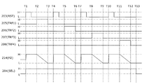
次に、図1で示した光センサ回路102の駆動について説明する。図2に光センサ回路102のタイミングチャートを示す。
Next, driving of the
なお、図2に示すタイミングチャートにおいて、高レベル電源電位VDDを、”H”で、低レベル電源電位VSSを、”L”で表すものとする。 In the timing chart shown in FIG. 2, the high level power supply potential VDD is represented by “H” and the low level power supply potential VSS is represented by “L”.
時刻T1において、リセット信号線(RST)203の電位を、”H”とする。(第1のリセット)。リセットトランジスタ108のゲートは、”H”となるため、リセットトランジスタ108がオン状態となる。この時、ノード214の電位が、”L”から”H”に切り替わる。一定期間の後、リセット信号線(RST)203の電位を、”H”から”L”とする。
At time T1, the potential of the reset signal line (RST) 203 is set to “H”. (First reset). Since the gate of the
時刻T2において、信号線(TRF1)205の電位を、”H”とする。この時、信号線(TRF1)205と電気的に接続された転送トランジスタ107のゲートが”H”になるため、転送トランジスタ107がオン状態となる。該トランジスタと電気的に接続された受光素子106と、ノード214とが導通し、ノード214の電位が”H”より低下し始める。
At time T2, the potential of the signal line (TRF1) 205 is set to “H”. At this time, the gate of the
時刻T3において、信号線(TRF1)205の電位を、”H”から”L”とする。この時、転送トランジスタ107がオフ状態となる。ノード214の電位は、時刻T3以後は、再びリセットトランジスタ108のゲートが”H”となるまで一定となる。本実施の形態では、この時のノード214の電位は低レベル電源電位VSSとなっている。
At time T3, the potential of the signal line (TRF1) 205 is changed from “H” to “L”. At this time, the
時刻T2〜時刻T3の間、受光素子106に照射される光の量に応じて、受光素子106の抵抗は変化し、受光素子106と、ノード214との間に電流が流れる。流れた電流に応じた電荷がトランジスタ107を介してノード214に蓄積される。
Between time T <b> 2 and time T <b> 3, the resistance of the
時刻T4において、再びリセット信号線(RST)203の電位を、”H”とする。(第2のリセット)。リセットトランジスタ108のゲートは、”H”となるため、リセットトランジスタ108がオン状態となる。この時、ノード214の電位が、”L”から”H”に切り替わる。一定期間の後、リセット信号線(RST)203の電位を、”H”から”L”とする。
At time T4, the potential of the reset signal line (RST) 203 is set to “H” again. (Second reset). Since the gate of the
時刻T5において、信号線(TRF2)206の電位を、”H”とする。この時、信号線(TRF2)206と電気的に接続された転送トランジスタ107のゲートが”H”になるため、転送トランジスタ107がオン状態となる。該トランジスタと電気的に接続された受光素子106と、ノード214とが導通し、ノード214の電位が”H”より低下し始める。
At time T5, the potential of the signal line (TRF2) 206 is set to “H”. At this time, since the gate of the
時刻T6において、信号線(TRF2)206の電位を、”H”から”L”とする。この時、転送トランジスタ107がオフ状態となる。ノード214の電位は、時刻T6以後は、再びリセットトランジスタ108のゲートが”H”となるまで一定となる。本実施の形態では、この時のノード214の電位は低レベル電源電位VSSとなっている。
At time T6, the potential of the signal line (TRF2) 206 is changed from “H” to “L”. At this time, the
時刻T5〜時刻T6の間、受光素子106に照射される光の量に応じて、受光素子106の抵抗は変化し、受光素子106と、ノード214との間に電流が流れる。流れた電流に応じた電荷がトランジスタ107を介してノード214に蓄積される。
Between time T <b> 5 and time T <b> 6, the resistance of the
時刻T7において、再びリセット信号線(RST)203の電位を、”H”とする。(第3のリセット)。リセットトランジスタ108のゲートは、”H”となるため、リセットトランジスタ108がオン状態となる。この時、ノード214の電位が、”L”から”H”に切り替わる。一定期間の後、リセット信号線(RST)203の電位を、”H”から”L”とする。
At time T7, the potential of the reset signal line (RST) 203 is set to “H” again. (Third reset). Since the gate of the
時刻T8において、信号線(TRF3)207の電位を、”H”とする。この時、信号線(TRF3)207と電気的に接続された転送トランジスタ107のゲートが”H”になるため、転送トランジスタ107がオン状態となる。該トランジスタと電気的に接続された受光素子106と、ノード214とが導通し、ノード214の電位が”H”より低下し始める。
At time T8, the potential of the signal line (TRF3) 207 is set to “H”. At this time, the gate of the
時刻T9において、信号線(TRF3)207の電位を、”H”から”L”とする。この時、転送トランジスタ107がオフ状態となる。ノード214の電位は、時刻T9以後は、再びリセットトランジスタ108のゲートが”H”となるまで一定となる。本実施の形態では、この時のノード214の電位は低レベル電源電位VSSとなっている。
At time T9, the potential of the signal line (TRF3) 207 is changed from “H” to “L”. At this time, the
時刻T8〜時刻T9の間、受光素子106に照射される光の量に応じて、受光素子106の抵抗は変化し、受光素子106と、ノード214との間に電流が流れる。流れた電流に応じた電荷がトランジスタ107を介してノード214に蓄積される。
Between time T <b> 8 and time T <b> 9, the resistance of the
時刻T10において、再びリセット信号線(RST)203の電位を、”H”とする。(第4のリセット)。リセットトランジスタ108のゲートは、”H”となるため、リセットトランジスタ108がオン状態となる。この時、ノード214の電位が、”L”から”H”に切り替わる。一定期間の後、リセット信号線(RST)203の電位を、”H”から”L”とする。
At time T10, the potential of the reset signal line (RST) 203 is set to “H” again. (Fourth reset). Since the gate of the
時刻T11において、信号線(TRF4)208の電位を、”H”とする。この時、信号線(TRF4)208と電気的に接続された転送トランジスタ107のゲートが”H”になるため、転送トランジスタ107がオン状態となる。該トランジスタと電気的に接続された受光素子106と、ノード214とが導通し、ノード214の電位が”H”より低下し始める。
At time T11, the potential of the signal line (TRF4) 208 is set to “H”. At this time, the gate of the
時刻T12において、信号線(TRF4)208の電位を、”H”から”L”とする。この時、転送トランジスタ107がオフ状態となる。ノード214の電位は、時刻T12以後は、再びリセットトランジスタ108のゲートが”H”となるまで一定となる。本実施の形態では、この時のノード214の電位は低レベル電源電位VSSとなっている。
At time T12, the potential of the signal line (TRF4) 208 is changed from “H” to “L”. At this time, the
時刻T11〜時刻T12の間、受光素子106に照射される光の量に応じて、受光素子106の抵抗は変化し、受光素子106と、ノード214との間に電流が流れる。流れた電流に応じた電荷がトランジスタ107を介してノード214に蓄積される。
Between time T <b> 11 and time T <b> 12, the resistance of the
また、期間T1で選択信号線(SEL)204の電位は、”L”から”H”となり、期間T1〜期間T13までの間、”H”電位を維持する。期間T13で選択信号線(SEL)204の電位は、”H”から”L”となる。これにより、期間T1〜期間T13までの間、選択トランジスタ110は、常にオン状態となっている。従って、増幅トランジスタ109のゲートの電位、即ちノード214の電位に応じて、フォトセンサ出力信号線(OUT)210から、出力信号が随時出力される。
In addition, the potential of the selection signal line (SEL) 204 is changed from “L” to “H” in the period T1, and the “H” potential is maintained from the period T1 to the period T13. In the period T13, the potential of the selection signal line (SEL) 204 is changed from “H” to “L”. Thus, the
上述の駆動方法によれば、4個の受光素子に対して、リセットトランジスタ、増幅トランジスタ、選択トランジスタが、それぞれ1個ずつしかなくても、これらを共有する4個の受光素子、それぞれに対応する出力信号を、フォトセンサ出力信号線(OUT)210から順次取り出すことが可能になる。 According to the driving method described above, even if there are only one reset transistor, one amplification transistor, and one selection transistor for each of the four light receiving elements, each of the four light receiving elements sharing these elements corresponds to each of the four light receiving elements. Output signals can be sequentially extracted from the photosensor output signal line (OUT) 210.
なお、本実施の形態は、本明細書で示す他の実施の形態と適宜組み合わせることができる。 Note that this embodiment can be combined with any of the other embodiments described in this specification as appropriate.
(実施の形態2)
本実施の形態では、本発明の一態様に係る半導体装置が反射型液晶表示領域を有する場合について説明する。
(Embodiment 2)
In this embodiment, the case where a semiconductor device according to one embodiment of the present invention includes a reflective liquid crystal display region will be described.
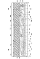
受光素子の半導体層として非単結晶半導体層を、トランジスタの半導体層として酸化物半導体層を用いる反射型液晶表示装置の作製方法の一例について、図4を用いて説明する。図4におけるA−Bまでの領域は、単位画素の一部分を、C−Dまでの領域は、光センサ回路の一部分を示している。なお、単位画素及び光センサ回路は該構成に限定されない。 An example of a method for manufacturing a reflective liquid crystal display device using a non-single-crystal semiconductor layer as a semiconductor layer of a light-receiving element and an oxide semiconductor layer as a semiconductor layer of a transistor will be described with reference to FIGS. The area up to AB in FIG. 4 shows a part of the unit pixel, and the area up to CD shows a part of the photosensor circuit. Note that the unit pixel and the optical sensor circuit are not limited to this configuration.
まず、基板230上に導電膜を形成した後、当該導電膜を用いて、走査線227、容量配線224、信号線208、電源線264を形成する。また図示しない、選択線、電極層、リセット線、グランド線等を形成する。本実施の形態では基板230としてガラス基板を用いる。酸化物半導体層を用いるトランジスタのプロセス温度は400℃以下という低い温度にできるため、基板230として、ガラス基板の他に、プラスティック基板を用いてもよい。
First, after a conductive film is formed over the
下地膜となる絶縁膜を基板230と導電膜との間に設けてもよい。下地膜は、基板230からの不純物元素の拡散を防止する機能があり、窒化シリコン膜、酸化シリコン膜、窒化酸化シリコン膜、又は酸化窒化シリコン膜から選ばれた一又は複数の膜による積層構造により形成することができる。
An insulating film serving as a base film may be provided between the
また、導電膜は、モリブデン、チタン、タンタル、タングステン、アルミニウム、銅、ネオジム、スカンジウム等の金属材料又はこれらを主成分とする合金材料を用いて、単層で又は積層して形成することができる。 The conductive film can be formed as a single layer or a stacked layer using a metal material such as molybdenum, titanium, tantalum, tungsten, aluminum, copper, neodymium, or scandium, or an alloy material containing any of these as a main component. .
次いで、これらの配線を覆う絶縁層を形成し、後に形成される配線と交差する部分にのみ絶縁層231を残して選択的にエッチングを行う。本実施の形態では、絶縁層231は膜厚600nmの酸化窒化珪素膜を用いる。
Next, an insulating layer covering these wirings is formed, and etching is selectively performed leaving the insulating
次いで、ゲート絶縁層232及び酸化物半導体膜を形成する。
Next, a
ゲート絶縁層232は、窒素を含むシリコン膜を含んで構成されていてもよい。窒素を含むシリコン膜は、酸化シリコン膜と比較して比誘電率が高く、同等の静電容量を得るのに必要な膜厚が大きいため、ゲート絶縁層を物理的に厚膜化することができる。よって、トランジスタの絶縁耐圧の低下を抑制、さらには絶縁耐圧を向上させて、半導体装置の静電破壊を抑制することができる。
The
ゲート絶縁層232の膜厚は、少なくとも後述する酸化物絶縁層よりも厚い膜厚で設けるものとし、325nm以上550nm以下とすることが好ましく、355nm以上550nm以下とすることがより好ましい。
The thickness of the
窒素を含むシリコン膜としては、例えば、窒化シリコン膜、窒化酸化シリコン膜、酸化窒化シリコン膜が挙げられるが、窒素の含有量が多い程高い比誘電率を有するため、窒化シリコン膜を適用することが好ましい。また、酸化シリコンのエネルギーギャップが8eVであるのに対して窒化シリコンのエネルギーギャップは5.5eVと小さく、それに応じて固有抵抗も小さいため、窒化シリコン膜を用いることでより高いESD耐性を付与することが可能となる。さらに、窒化シリコン膜をCVD法で成膜する場合、窒化酸化シリコン膜等の酸素と窒素を含むシリコン膜をCVD法で成膜する場合に適用される温室効果ガスであるN2Oガスを用いる必要がない。なお、本明細書中において、酸化窒化シリコン膜とは、その組成として、窒素よりも酸素の含有量が多い膜を指し、窒化酸化シリコン膜とは、その組成として、酸素よりも窒素の含有量が多い膜を指す。 As the silicon film containing nitrogen, for example, a silicon nitride film, a silicon nitride oxide film, and a silicon oxynitride film can be given. However, since the higher the nitrogen content, the higher the dielectric constant, the silicon nitride film should be applied. Is preferred. Further, since the energy gap of silicon oxide is 8 eV, the energy gap of silicon nitride is as small as 5.5 eV, and the specific resistance is accordingly small. Therefore, higher ESD resistance is imparted by using a silicon nitride film. It becomes possible. Further, when a silicon nitride film is formed by a CVD method, N 2 O gas which is a greenhouse gas applied when a silicon film containing oxygen and nitrogen such as a silicon nitride oxide film is formed by a CVD method is used. There is no need. Note that in this specification, a silicon oxynitride film refers to a film having a higher oxygen content than nitrogen as a composition, and a silicon nitride oxide film includes a nitrogen content as compared to oxygen as a composition. Refers to membranes with a lot of
上記酸化物半導体膜は、化学式InMO3(ZnO)m(m>0)で表記される酸化物薄膜を用いることができる。ここで、Mは、Ga、Al、MnおよびCoから選ばれた一または複数の金属元素を示す。例えばMとして、Ga、Ga及びAl、Ga及びMn、またはGa及びCoなどがある。また、上記酸化物薄膜にSiO2を含んでもよい。 As the oxide semiconductor film, an oxide thin film represented by a chemical formula of InMO 3 (ZnO) m (m> 0) can be used. Here, M represents one or more metal elements selected from Ga, Al, Mn, and Co. For example, M includes Ga, Ga and Al, Ga and Mn, or Ga and Co. Further, the oxide thin film may contain SiO 2 .
また、酸化物薄膜をスパッタリング法で作製するためのターゲットとしては、例えば、組成として、In2O3:Ga2O3:ZnO=1:1:1[mol数比]の酸化物ターゲットを用い、In−Ga−Zn−O膜を成膜する。また、このターゲットの材料及び組成に限定されず、例えば、In2O3:Ga2O3:ZnO=1:1:2[mol数比]の酸化物ターゲットを用いてもよい。なお、ここで、例えば、In−Ga−Zn−O膜とは、インジウム(In)、ガリウム(Ga)、亜鉛(Zn)を有する酸化物膜、という意味であり、その化学量論比はとくに問わない。 As a target for forming an oxide thin film by a sputtering method, for example, an oxide target having a composition of In 2 O 3 : Ga 2 O 3 : ZnO = 1: 1: 1 [molar ratio] is used. An In—Ga—Zn—O film is formed. Without limitation to the material and the composition of the target, for example, In 2 O 3: Ga 2 O 3: ZnO = 1: 1: 2 may be an oxide target [mol ratio]. Note that here, for example, an In—Ga—Zn—O film means an oxide film containing indium (In), gallium (Ga), and zinc (Zn), and the stoichiometric ratio is particularly high. It doesn't matter.
なおゲート絶縁層232及び上記酸化物半導体膜との間に、酸化物絶縁層を設けてもよい。
Note that an oxide insulating layer may be provided between the
当該酸化物絶縁層は、上記酸化物半導体膜の構成元素から選択される一又は複数の金属元素を含んで構成される。このような材料を用いて当該酸化物絶縁層を構成することで、上記酸化物半導体膜との界面を安定化させることができ、該界面に電荷がトラップされることを抑制することができる。よって、トランジスタの劣化、特に光劣化を防止し、信頼性の高いトランジスタとすることができる。 The oxide insulating layer includes one or more metal elements selected from the constituent elements of the oxide semiconductor film. When the oxide insulating layer is formed using such a material, the interface with the oxide semiconductor film can be stabilized, and trapping of charges at the interface can be suppressed. Therefore, deterioration of the transistor, in particular, light deterioration can be prevented and a highly reliable transistor can be obtained.
具体的には、当該酸化物絶縁層として、例えば、酸化ガリウム膜(GaOxとも表記する、なお、xは自然数とは限らず、非自然数を含む)、酸化ガリウム亜鉛膜(Ga2ZnxOy(x=1〜5)とも表記する)、Ga2O3(Gd2O3)膜、ガリウムの含有量が多く、且つ、インジウムの含有量の少ないIn−Ga−Zn系酸化物膜などを設けることが好ましい。 Specifically, as the oxide insulating layer, for example, a gallium oxide film (also expressed as GaO x , where x is not limited to a natural number but includes a non-natural number), a gallium zinc oxide film (Ga 2 Zn x O y (x = 1 to 5)), a Ga 2 O 3 (Gd 2 O 3 ) film, an In—Ga—Zn-based oxide film having a high gallium content and a low indium content, etc. Is preferably provided.
当該酸化物絶縁層と上記酸化物半導体膜の構成元素を同一とし、両者の組成を異ならせてもよい。例えば、当該酸化物半導体膜として、In−Ga−Zn系酸化物半導体層を用いる場合、インジウム(In)とガリウム(Ga)の比率によって、エネルギーギャップを制御することが可能であるため、上記酸化物半導体膜の原子数比をIn:Ga:Zn=1:1:1、又は、In:Ga:Zn=3:1:2として、当該酸化物絶縁層の原子数比をIn:Ga:Zn=1:3:2とすればよい。なお、当該酸化物絶縁層及び上記酸化物半導体膜は、スパッタリング法によって形成することができ、スパッタリングターゲットにインジウムを含有すると成膜時のパーティクルの発生を低減することができる。よって、インジウムを含む酸化物絶縁層及びインジウムを含む酸化物半導体膜とすることが好ましい。 The constituent elements of the oxide insulating layer and the oxide semiconductor film may be the same, and the compositions of the two may be different. For example, when an In—Ga—Zn-based oxide semiconductor layer is used as the oxide semiconductor film, the energy gap can be controlled by the ratio of indium (In) to gallium (Ga); The atomic ratio of the oxide semiconductor layer is In: Ga: Zn = 1: 1: 1 or In: Ga: Zn = 3: 1: 2, and the atomic ratio of the oxide insulating layer is In: Ga: Zn. = 1: 3: 2. Note that the oxide insulating layer and the oxide semiconductor film can be formed by a sputtering method. When the sputtering target contains indium, generation of particles during film formation can be reduced. Therefore, an oxide insulating layer containing indium and an oxide semiconductor film containing indium are preferable.
上記酸化物半導体膜(第1の酸化物半導体膜とする)上に、新たに第2の酸化物半導体膜を形成し、酸化物半導体膜を積層構造としてもよい。図4では、第1の酸化物半導体膜から酸化物半導体層233、第2の酸化物半導体膜から酸化物半導体層228を形成する例を示している。
A second oxide semiconductor film may be newly formed over the oxide semiconductor film (referred to as a first oxide semiconductor film), and the oxide semiconductor film may have a stacked structure. FIG. 4 illustrates an example in which the
第1の酸化物半導体膜と第2の酸化物半導体膜は、構成元素を同一とし、両者の組成を異ならせることが好ましい。第1の酸化物半導体膜と第2の酸化物半導体膜としてインジウム及びガリウムを含む酸化物半導体膜を形成する場合、ゲート電極に近い側(チャネル側)の第1の酸化物半導体膜のインジウムとガリウムの含有率をIn>Gaとするとよい。またゲート電極から遠い側(バックチャネル側)の第2の酸化物半導体膜のインジウムとガリウムの含有率をIn≦Gaとするとよい。 It is preferable that the first oxide semiconductor film and the second oxide semiconductor film have the same constituent elements and have different compositions. In the case where an oxide semiconductor film containing indium and gallium is formed as the first oxide semiconductor film and the second oxide semiconductor film, indium in the first oxide semiconductor film on the side close to the gate electrode (channel side) The content of gallium is preferably In> Ga. The content ratio of indium and gallium in the second oxide semiconductor film far from the gate electrode (back channel side) is preferably In ≦ Ga.
酸化物半導体では主として重金属のs軌道がキャリア伝導に寄与しており、インジウムの含有率を多くすることによりs軌道のオーバーラップが多くなる傾向があるため、In>Gaの組成となる酸化物はIn≦Gaの組成となる酸化物と比較して高い移動度を備える。また、GaはInと比較して酸素欠損の形成エネルギーが大きく酸素欠損が生じにくいため、In≦Gaの組成となる酸化物はIn>Gaの組成となる酸化物と比較して安定した特性を備える。 In oxide semiconductors, heavy metal s orbitals mainly contribute to carrier conduction, and increasing the indium content tends to increase the overlap of s orbitals. Compared with an oxide having a composition of In ≦ Ga, high mobility is provided. In addition, since Ga has a larger energy generation energy of oxygen deficiency than In, and oxygen deficiency is less likely to occur, an oxide having a composition of In ≦ Ga has stable characteristics compared to an oxide having a composition of In> Ga. Prepare.
チャネル側にIn>Gaの組成となる酸化物半導体を適用し、バックチャネル側にIn≦Gaの組成となる酸化物半導体を適用することで、トランジスタの移動度および信頼性をさらに高めることが可能となる。例えば、第1の酸化物半導体膜の原子数比をIn:Ga:Zn=3:1:2とし、第2の酸化物半導体膜の原子数比をIn:Ga:Zn=1:1:1としてもよい。 By using an oxide semiconductor with an In> Ga composition on the channel side and an oxide semiconductor with an In ≦ Ga composition on the back channel side, the mobility and reliability of the transistor can be further improved. It becomes. For example, the atomic ratio of the first oxide semiconductor film is In: Ga: Zn = 3: 1: 2, and the atomic ratio of the second oxide semiconductor film is In: Ga: Zn = 1: 1: 1. It is good.
なお、第1の酸化物半導体膜に接する酸化物絶縁層の構成元素を第1の酸化物半導体膜と同一とし、組成を異ならせることで酸化物絶縁層の導電性を低下させると、両者の界面をより安定化させることができるため、好ましい。第2の酸化物半導体膜に酸化物絶縁層が接する場合も同様である。 Note that when the constituent elements of the oxide insulating layer in contact with the first oxide semiconductor film are the same as those of the first oxide semiconductor film and the conductivity of the oxide insulating layer is reduced by changing the composition, This is preferable because the interface can be further stabilized. The same applies to the case where the oxide insulating layer is in contact with the second oxide semiconductor film.
また、第1の酸化物半導体膜と第2の酸化物半導体膜に、結晶性の異なる酸化物半導体を適用してもよい。すなわち、単結晶酸化物半導体、多結晶酸化物半導体、微結晶酸化物半導体、非晶質酸化物半導体、またはCAAC−OS膜を適宜組み合わせた構成としてもよい。また、第1の酸化物半導体膜と第2の酸化物半導体膜の少なくともどちらか一方に非晶質酸化物半導体を適用すると、第1の酸化物半導体膜と第2の酸化物半導体膜の積層構造の内部応力や外部からの応力を緩和し、トランジスタの特性ばらつきが低減され、また、トランジスタの信頼性をさらに高めることが可能となる。 Alternatively, oxide semiconductors having different crystallinities may be used for the first oxide semiconductor film and the second oxide semiconductor film. In other words, a single crystal oxide semiconductor, a polycrystalline oxide semiconductor, a microcrystalline oxide semiconductor, an amorphous oxide semiconductor, or a CAAC-OS film may be combined as appropriate. In addition, when an amorphous oxide semiconductor is applied to at least one of the first oxide semiconductor film and the second oxide semiconductor film, the first oxide semiconductor film and the second oxide semiconductor film are stacked. The internal stress of the structure and the external stress are alleviated, the characteristic variation of the transistor is reduced, and the reliability of the transistor can be further improved.
一方で、非晶質酸化物半導体は水素などのドナーとなる不純物を吸収しやすく、また、酸素欠損が生じやすいためn型化されやすい。このため、チャネル側の第1の酸化物半導体膜は、CAAC−OS膜などの結晶性を有する酸化物半導体を適用することが好ましい。 On the other hand, an amorphous oxide semiconductor easily absorbs an impurity serving as a donor such as hydrogen, and oxygen vacancies easily occur. Therefore, the first oxide semiconductor film on the channel side is preferably formed using a crystalline oxide semiconductor such as a CAAC-OS film.
酸化物半導体は、非単結晶であって、そのa−b面に垂直な方向から見て、三角形、六角形、正三角形、又は正六角形の原子配列を有し、且つ、c軸に垂直な方向から見て、金属原子が層状、又は金属原子と酸素原子が層状に配列した相を含む酸化物である。なお、本明細書等では、c軸配向結晶を含む酸化物半導体をCAAC−OS(C AxisAligned Crystalline Oxide Semiconductor)と呼ぶ。 An oxide semiconductor is a non-single crystal and has a triangular, hexagonal, equilateral triangle, or equilateral hexagonal atomic arrangement when viewed from the direction perpendicular to the ab plane, and is perpendicular to the c-axis. When viewed from the direction, the oxide includes a phase in which metal atoms are arranged in layers, or metal atoms and oxygen atoms are arranged in layers. Note that in this specification and the like, an oxide semiconductor including a c-axis aligned crystal is referred to as a CAAC-OS (C Axis Crystallized Oxide Semiconductor).
CAAC−OSは単結晶ではないが、非晶質のみから形成されているものでもない。また、CAAC−OSは結晶部分を含むが、1つの結晶部分と他の結晶部分を明確に判別できないこともある。 A CAAC-OS is not a single crystal but is not formed of only an amorphous substance. In addition, although the CAAC-OS includes a crystal part, one crystal part and another crystal part may not be clearly distinguished.
CAAC−OSに酸素が含まれる場合、酸素の一部は窒素で置換されてもよい。また、CAAC−OSを構成する個々の結晶部分のc軸は一定の方向(例えば、CAAC−OSが形成される基板面、CAAC−OSの表面などに垂直な方向)に揃っていてもよい。または、CAAC−OSを構成する個々の結晶部分のab面の法線は一定の方向(例えば、CAAC−OSが形成される基板面、CAAC−OSの表面などに垂直な方向)を向いていてもよい。 In the case where oxygen is included in the CAAC-OS, part of oxygen may be replaced with nitrogen. In addition, the c-axis of each crystal part included in the CAAC-OS may be aligned in a certain direction (eg, a direction perpendicular to a substrate surface on which the CAAC-OS is formed, the surface of the CAAC-OS, or the like). Alternatively, the normal line of the ab plane of each crystal part included in the CAAC-OS faces a certain direction (for example, a direction perpendicular to the substrate surface on which the CAAC-OS is formed, the surface of the CAAC-OS, or the like). Also good.
このようなCAAC−OSの例として、層状に形成され、層表面、または支持する基板面に垂直な方向から観察すると、三角形または六角形の原子配列が認められ、且つその層の断面を観察すると金属原子または金属原子と酸素原子(または窒素原子)の層状配列が認められる材料を挙げることもできる。 As an example of such a CAAC-OS, when observed from a direction perpendicular to the surface of the layer or the supporting substrate, a triangular or hexagonal atomic arrangement is observed, and a cross section of the layer is observed. A material in which a layered arrangement of metal atoms or metal atoms and oxygen atoms (or nitrogen atoms) is recognized can also be mentioned.
CAAC−OS膜は、例えば、多結晶である酸化物半導体スパッタリング用ターゲットを用い、スパッタリング法によって成膜する。当該スパッタリング用ターゲットにイオンが衝突すると、スパッタリング用ターゲットに含まれる結晶領域がa−b面から劈開し、a−b面に平行な面を有する平板状またはペレット状のスパッタリング粒子として剥離することがある。この場合、当該平板状のスパッタリング粒子が、結晶状態を維持したまま基板に到達することで、スパッタリング用ターゲットの結晶状態が基板に転写され、CAAC−OS膜を成膜することができる。 For example, the CAAC-OS film is formed by a sputtering method using a polycrystalline oxide semiconductor sputtering target. When ions collide with the sputtering target, the crystal region included in the sputtering target is cleaved from the ab plane, and may be separated as flat or pellet-like sputtering particles having a plane parallel to the ab plane. is there. In this case, when the flat-plate-like sputtered particles reach the substrate while maintaining the crystal state, the crystal state of the sputtering target is transferred to the substrate, and a CAAC-OS film can be formed.
また、CAAC−OS膜を成膜するために、以下の条件を適用することが好ましい。 In order to form the CAAC-OS film, the following conditions are preferably applied.
成膜時の不純物濃度を低減することで、不純物によって結晶状態が崩れることを抑制できる。例えば、成膜室内に存在する不純物(水素、水、二酸化炭素および窒素など)を低減すればよい。また、成膜ガス中の不純物を低減すればよい。具体的には、露点が−80℃以下、好ましくは−100℃以下である成膜ガスを用いる。 By reducing the impurity concentration at the time of film formation, the crystal state can be prevented from being broken by the impurities. For example, impurities (hydrogen, water, carbon dioxide, nitrogen, and the like) existing in the deposition chamber may be reduced. In addition, impurities in the deposition gas may be reduced. Specifically, a deposition gas having a dew point of −80 ° C. or lower, preferably −100 ° C. or lower is used.
また、成膜時の基板加熱温度を高めることで、基板付着後にスパッタリング粒子のマイグレーションが起こる。具体的には、基板加熱温度を100℃以上740℃以下、好ましくは200℃以上500℃以下として成膜する。成膜時の基板加熱温度を高めることで、平板状のスパッタリング粒子が基板に到達した場合、基板上でマイグレーションが起こり、平らな面が基板に付着する。 Further, by increasing the substrate heating temperature during film formation, migration of the sputtered particles occurs after the substrate adheres. Specifically, the film is formed at a substrate heating temperature of 100 ° C. to 740 ° C., preferably 200 ° C. to 500 ° C. By increasing the substrate heating temperature during film formation, when flat sputtered particles reach the substrate, migration occurs on the substrate, and a flat surface adheres to the substrate.
また、成膜ガス中の酸素割合を高め、電力を最適化することで成膜時のプラズマダメージを軽減すると好ましい。成膜ガス中の酸素割合は、30体積%以上、好ましくは100体積%とする。 In addition, it is preferable to reduce plasma damage during film formation by increasing the oxygen ratio in the film formation gas and optimizing electric power. The oxygen ratio in the deposition gas is 30% by volume or more, preferably 100% by volume.
スパッタリング用ターゲットの一例として、In−Ga−Zn−O化合物ターゲットについて以下に示す。 As an example of the sputtering target, an In—Ga—Zn—O compound target is described below.
InOX粉末、GaOY粉末およびZnOZ粉末を所定の比率で混合し、加圧処理後、1000℃以上1500℃以下の温度で加熱処理をすることで多結晶であるIn−Ga−Zn−O化合物ターゲットとする。なお、X、YおよびZは任意の正数である。ここで、所定の比率は、例えば、InOX粉末、GaOY粉末およびZnOZ粉末が、2:2:1、8:4:3、3:1:1、1:1:1、4:2:3または3:1:2のmol数比である。なお、粉末の種類、およびその混合する比率は、作製するスパッタリング用ターゲットによって適宜変更すればよい。 In-Ga-Zn-O which is polycrystalline by mixing InO X powder, GaO Y powder and ZnO Z powder at a predetermined ratio, and after heat treatment at a temperature of 1000 ° C to 1500 ° C. The compound target. X, Y and Z are arbitrary positive numbers. Here, the predetermined ratio is, for example, 2: 2: 1, 8: 4: 3, 3: 1: 1, 1: 1: 1, 4: 2 for InO X powder, GaO Y powder, and ZnO Z powder. : 3 or 3: 1: 2 mol number ratio. Note that the type of powder and the mixing ratio may be changed as appropriate depending on the sputtering target to be manufactured.
また、バックチャネル側の第2の酸化物半導体膜に非晶質酸化物半導体を用いると、後に形成されるソース電極層及びドレイン電極層形成時のエッチング処理により酸素欠損が生じ、n型化されやすい。第2の酸化物半導体膜には結晶性を有する酸化物半導体を適用することが好ましい。 In addition, when an amorphous oxide semiconductor is used for the second oxide semiconductor film on the back channel side, oxygen vacancies are generated due to an etching process in forming a source electrode layer and a drain electrode layer to be formed later, and the n-type is formed. Cheap. An oxide semiconductor having crystallinity is preferably used for the second oxide semiconductor film.
本実施の形態では、ゲート絶縁層232として膜厚100nmの酸化窒化珪素膜を用い、酸化物半導体膜として膜厚30nmのIn−Ga−Zn−O膜を用いる。
In this embodiment, a silicon oxynitride film with a thickness of 100 nm is used as the
上記酸化物半導体膜(第1の半導体膜)を用いて、ゲート絶縁層232を介して、走査線227と重なる酸化物半導体層233を形成する。
With the use of the oxide semiconductor film (first semiconductor film), an
次いで、酸化物半導体層に第1の加熱処理を行う。この第1の加熱処理によって酸化物半導体層の脱水化または脱水素化を行うことができる。第1の加熱処理の温度は、350℃以上基板の歪み点未満とする。本実施の形態では、RTA(Rapid Thermal Anneal)装置を用い、窒素雰囲気下で650℃、6分の加熱処理を行った後、大気に触れることなく、加熱処理装置の一つである電気炉に基板を導入し、酸化物半導体層に対して窒素雰囲気下450℃において1時間の加熱処理を行った後、大気に触れないように酸化物半導体層の成膜室に移動させて酸化物半導体層への水や水素の再混入を防ぎ、酸化物半導体層を得る。 Next, first heat treatment is performed on the oxide semiconductor layer. Through the first heat treatment, the oxide semiconductor layer can be dehydrated or dehydrogenated. The temperature of the first heat treatment is 350 ° C. or higher and lower than the strain point of the substrate. In this embodiment, after performing a heat treatment at 650 ° C. for 6 minutes in a nitrogen atmosphere using a RTA (Rapid Thermal Anneal) apparatus, an electric furnace which is one of the heat treatment apparatuses is exposed to the atmosphere without being exposed to the air. After the substrate is introduced and the oxide semiconductor layer is subjected to heat treatment at 450 ° C. for 1 hour in a nitrogen atmosphere, the oxide semiconductor layer is moved to the oxide semiconductor layer deposition chamber so as not to be exposed to the air. Oxide semiconductor layer is obtained by preventing re-mixing of water and hydrogen into the substrate.
次いで、ゲート絶縁層232、及び酸化物半導体層上に、導電膜を形成する。導電膜としては、例えば、アルミニウム(Al)、クロム(Cr)、銅(Cu)、タンタル(Ta)、チタン(Ti)、モリブデン(Mo)、タングステン(W)から選ばれた元素を成分とする金属膜、または上述した元素の窒化物を成分とする合金膜か、上述した元素を組み合わせた合金膜等を用いることができる。本実施の形態において、導電膜は、膜厚100nmのチタン膜と、膜厚400nmのアルミニウム膜と、膜厚100nmのチタン膜との三層構造とする。
Next, a conductive film is formed over the
そして、導電膜上にレジストマスクを形成し、選択的にエッチングを行って、信号線260、電極層234、電極層273を形成する。
Then, a resist mask is formed over the conductive film and selective etching is performed, so that the
なお、トランジスタ221は、酸化物半導体層233を有し、走査線227をゲートとし、信号線260をソース電極層又はドレイン電極層の一方とし、電極層234をソース電極層又はドレイン電極層の他方とするトランジスタである。
Note that the
また、電極層234及び容量配線224は、間に挟まれたゲート絶縁層232を誘電体とし、保持容量222を形成する。
In addition, the
次いで、不活性ガス雰囲気下、または酸素ガス雰囲気下で第2の加熱処理(好ましくは200℃以上400℃以下)を行う。本実施の形態では、窒素雰囲気下で220℃、1時間の第2の加熱処理を行う。第2の加熱処理を行うと、酸化物半導体層の一部(チャネル形成領域)が絶縁層と接した状態で加熱される。 Next, second heat treatment (preferably at 200 ° C. to 400 ° C.) is performed in an inert gas atmosphere or an oxygen gas atmosphere. In this embodiment, the second heat treatment is performed at 220 ° C. for 1 hour in a nitrogen atmosphere. When the second heat treatment is performed, part of the oxide semiconductor layer (a channel formation region) is heated in contact with the insulating layer.
次いで保護絶縁層となる絶縁層237を形成し、電極層234に達する開口、電極層273に達する開口、電源線264に達する開口を形成する。本実施の形態において、絶縁層237は、スパッタ法により得られる膜厚300nmの酸化シリコン膜を用いる。
Next, an insulating
次いで、電極層273上に非単結晶半導体層240を成膜する。本実施の形態では、非単結晶半導体層240として、プラズマCVD法により、膜厚800nmのi型アモルファスシリコン層を成膜する。そして、非単結晶半導体層240を選択的にエッチングする。
Next, the non-single-
次いで感光性有機樹脂層を形成し、露光マスクで開口となる領域を露光し、別の露光マスクで凹凸となる領域を露光し、現像して部分的に凹凸を有する絶縁層241を形成する。本実施の形態では、感光性有機樹脂層として、アクリル樹脂を用い、膜厚を1.5μmとする。
Next, a photosensitive organic resin layer is formed, the region to be the opening is exposed with an exposure mask, the region with the unevenness is exposed with another exposure mask, and developed to form the insulating
次いで、反射性を有する導電膜を成膜し、当該反射性を有する導電膜を用いて、反射電極層242、接続電極層243を形成する。更に、接続電極層243に接し、非単結晶半導体層240に重畳するように、電極層278を形成する。電極層278は、ITO等の透光性を有する導電性材料などで形成され、非単結晶半導体層240に照射される光が透過される材料を用いることが好ましい。なお、反射電極層242、接続電極層243、電極層278を図4に示す。反射性を有する導電膜としてはアルミニウム(Al)、銀(Ag)、またはこれらの合金、例えばネオジム(Nd)を含むアルミニウム、Ag−Pd−Cu合金等を用いる。本実施の形態において、反射性を有する導電膜は、膜厚100nmのチタン(Ti)膜とその上に設けた膜厚300nmのアルミニウム(Al)膜の積層を用いる。次いで第3の加熱処理、本実施の形態では、窒素雰囲気下250℃、1時間を行う。そして、反射電極層242を覆う配向膜244を形成する。
Next, a reflective conductive film is formed, and the
以上の工程により、同一基板上に反射電極層242を有する画素、及び、非単結晶半導体層240を有する受光素子106を作製することができる。受光素子106は、一対の電極である電極層273及び接続電極層278との間に非単結晶半導体層240が挟まれた構成となる。
Through the above process, the pixel having the
そして、上述のようにして作製されたアクティブマトリクス基板と貼り合わせる対向基板を用意する。対向基板として、透光性を有する基板301を用い、基板301に、遮光層302(ブラックマトリクスとも呼ぶ)、反射電極層242上にカラーフィルタ303を形成する。遮光層302としては、チタン、クロムなどの反射率の低い金属膜、または、黒色顔料や黒色染料が含浸された有機樹脂膜などを用いることができる。カラーフィルタ303は、特定の波長領域の光を透過する有色層である。例えば、赤色の波長帯域の光を透過する赤色(R)の着色層、緑色の波長帯域の光を透過する緑色(G)の着色層、青色の波長帯域の光を透過する青色(B)の着色層などを用いることができる。
Then, a counter substrate to be bonded to the active matrix substrate manufactured as described above is prepared. A light-transmitting
また、非単結晶半導体層240上には、遮光層もカラーフィルタも形成しない。さらに、基板301、遮光層302、カラーフィルタ303を覆って、透光性を有する導電膜304を形成する。透光性を有する導電膜304として、酸化タングステンを含むインジウム酸化物、酸化タングステンを含むインジウム亜鉛酸化物、酸化チタンを含むインジウム酸化物、酸化チタンを含むインジウム錫酸化物、インジウム錫酸化物(以下、ITOと示す。)、インジウム亜鉛酸化物、酸化ケイ素を添加したインジウム錫酸化物、グラフェン等を用いればよい。さらに有機樹脂を用いた柱状スペーサを形成する。そして、最後に配向膜306で覆う。
Further, neither the light-blocking layer nor the color filter is formed over the non-single-
この対向基板をシール材を用いてアクティブマトリクス基板と貼り合わせ、一対の基板間に液晶層305を挟持する。対向基板の遮光層302は、反射電極層242の表示領域及び受光素子106のセンシング領域に重ならないように設ける。また、一対の基板の間隔を一定に保持するために、位置合わせを正確に行って対向基板に柱状スペーサを設ける。
This counter substrate is bonded to the active matrix substrate using a sealant, and the
以上説明したように、図4のような反射性を有する導電膜を画素電極とする半導体装置を作製することができる。 As described above, a semiconductor device in which a reflective conductive film as illustrated in FIG. 4 is used as a pixel electrode can be manufactured.
なお図4では、受光素子106は、電極層273、非単結晶半導体層240、及び接続電極層278が順に積層された構成である。すなわち、受光素子の一対の電極が非単結晶半導体層の上下に接して設けられている。受光素子の構成は、これに限定されず、受光素子の一対の電極は、非単結晶半導体層の同じ面に接して形成されていてもよい。
Note that in FIG. 4, the
なお、本実施の形態は、本明細書で示す他の実施の形態と適宜組み合わせることができる。 Note that this embodiment can be combined with any of the other embodiments described in this specification as appropriate.
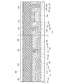
(実施の形態3)
本実施の形態では、本発明の一態様に係る半導体装置が透過型液晶表示領域を有する場合について説明する。なお本実施の形態において、実施の形態2と同じものは同じ符号で示し、その説明は省略する。
(Embodiment 3)
In this embodiment, the case where a semiconductor device according to one embodiment of the present invention includes a transmissive liquid crystal display region will be described. In the present embodiment, the same components as those in the second embodiment are denoted by the same reference numerals, and the description thereof is omitted.
受光素子の半導体層として非単結晶半導体層を、トランジスタの半導体層として酸化物半導体層を用いる透過型液晶表示装置の一例について、図5を用いて説明する。図5におけるA−Bまでの領域は、単位画素の一部分を、C−Dまでの領域は、光センサ回路の一部分を示している。なお、単位画素及び光センサ回路は該構成に限定されない。 An example of a transmissive liquid crystal display device using a non-single-crystal semiconductor layer as a semiconductor layer of a light-receiving element and an oxide semiconductor layer as a semiconductor layer of a transistor will be described with reference to FIGS. The area up to AB in FIG. 5 shows a part of the unit pixel, and the area up to CD shows a part of the photosensor circuit. Note that the unit pixel and the optical sensor circuit are not limited to this configuration.
図5に示す半導体装置の絶縁層241は、凹凸を設けず、平坦な面を有するように形成する。
The insulating
また図5に示す半導体装置では、図4の反射電極層242及び接続電極層243に代えて、透光性を有する導電膜にて、電極層262及び接続電極層263を形成する。アクティブマトリクス基板側に設けられたバックライトの光が受光素子106上の指などに反射し、反射した光が受光素子106に入射する。このようにして、光センサ回路によるセンシングを行うことができる。
In the semiconductor device illustrated in FIGS. 5A and 5B, the
以上説明したように、図5のような透光性を有する導電膜を画素電極とする半導体装置を得ることができる。 As described above, a semiconductor device in which a light-transmitting conductive film as illustrated in FIG. 5 is used as a pixel electrode can be obtained.
また、液晶層を挟む一対の電極を透光性を有する導電膜で形成し、当該一対の透光性を有する電極を、同一基板上に設けてもよい。これにより、IPSモード(In−Plane−Switching)などの横電界モードで液晶分子を駆動する半導体装置を得ることができる。 Alternatively, the pair of electrodes sandwiching the liquid crystal layer may be formed using a light-transmitting conductive film, and the pair of light-transmitting electrodes may be provided over the same substrate. Thus, a semiconductor device that drives liquid crystal molecules in a transverse electric field mode such as an IPS mode (In-Plane-Switching) can be obtained.
なお、本実施の形態は、本明細書で示す他の実施の形態と適宜組み合わせることができる。 Note that this embodiment can be combined with any of the other embodiments described in this specification as appropriate.
(実施の形態4)
本実施の形態では、画像表示を行う表示部を有する電気機器の一例を図6(A)及び図6(B)に示す。
(Embodiment 4)
In this embodiment, an example of an electric device including a display portion that performs image display is illustrated in FIGS.
図6に示す電気機器の構成例について説明する。電気機器1030の表示部1032はフォトセンサを用いるタッチ入力機能を有し、図6(A)に示すように表示部の領域1033にキーボードのボタン1031が複数表示される。表示部1032は表示領域全体を指しており、表示部の領域1033を含む。そして、使用者が所望のキーボードのボタンをタッチ入力し、表示部1032に入力結果の表示を行う。 A structural example of the electrical device illustrated in FIG. 6 will be described. The display portion 1032 of the electric device 1030 has a touch input function using a photosensor, and a plurality of keyboard buttons 1031 are displayed in the region 1033 of the display portion as illustrated in FIG. The display portion 1032 indicates the entire display area and includes a display portion area 1033. Then, the user touches and inputs a desired keyboard button, and the display unit 1032 displays the input result.
表示部の領域1033は静止画を表示しているため、書き込み時以外の期間では表示素子制御回路を非動作とすることで消費電力の節約ができる。 Since the display area 1033 displays a still image, power consumption can be saved by disabling the display element control circuit during a period other than writing.
電気機器1030を使用している様子の一例を示す。例えば、表示部の領域1033に表示されているキーボードボタンを使用者の指を用いて順次触れる、または非接触で文字入力を行い、その結果表示される文章を表示部の領域1033以外の領域に表示する。使用者が画面のキーボードから指をはずし、フォトセンサの出力信号の検出されない期間が一定時間経つと自動的に表示部の領域1033に表示されていたキーボード表示が消され、表示部の領域1033にも入力された文章の表示が行われ、画面一杯に入力された文章を使用者は確認することができる。再度入力する場合には、表示部1032に使用者の指を用いて触れる、または非接触でフォトセンサの出力信号を検出させることで再び表示部の領域1033にキーボードボタンを表示し、文字入力を行うことができる。 An example of a state in which the electric device 1030 is used is shown. For example, the keyboard buttons displayed in the area 1033 of the display unit are sequentially touched with a user's finger or non-contact character input is performed, and the resulting text is displayed in an area other than the area 1033 of the display unit. indicate. When the user removes his / her finger from the keyboard of the screen and a period in which the output signal of the photosensor is not detected passes for a certain period of time, the keyboard display that was displayed in the display area 1033 automatically disappears, and the display area 1033 The displayed text is also displayed, and the user can check the text that has been input to the full screen. When inputting again, the display unit 1032 is touched with a finger of the user, or the output signal of the photo sensor is detected in a non-contact manner so that the keyboard button is displayed again in the area 1033 of the display unit, and character input is performed. It can be carried out.
また、自動的ではなく、使用者が切り換えスイッチ1034を押すことによって、キーボード表示をなくし、図6(B)に示すように表示部1032の全体を静止画とすることもできる。また、電源スイッチ1035を押して電源を切っても、静止画を長時間維持することができる。また、キーボード表示スイッチ1036を押すことによってキーボードを表示し、タッチ入力可能な状態とすることができる。 Further, instead of automatically, the user can press the changeover switch 1034 to eliminate the keyboard display, and the entire display portion 1032 can be a still image as shown in FIG. 6B. Even if the power switch 1035 is pressed to turn off the power, the still image can be maintained for a long time. Further, the keyboard can be displayed by pressing the keyboard display switch 1036 so that touch input is possible.
また、切り換えスイッチ1034、電源スイッチ1035、及びキーボード表示スイッチ1036は、表示部1032にそれぞれスイッチボタンとして表示し、表示されたスイッチボタンに触れることで、各操作を行ってもよい。 The changeover switch 1034, the power switch 1035, and the keyboard display switch 1036 may be displayed as switch buttons on the display portion 1032 and may be operated by touching the displayed switch buttons.
また、表示部の領域1033は静止画を表示することに限定されず、一時的、または部分的に動画表示してもよい。例えば、キーボードボタンの表示位置を使用者の好みに合わせて一時的に変更する、または非接触で入力した場合に入力されたかどうかが分かるように対応するキーボードボタンのみに部分的に表示の変化を与えてもよい。 Further, the display area 1033 is not limited to displaying a still image, and may display a moving image temporarily or partially. For example, the display position of the keyboard button is temporarily changed according to the user's preference, or the display change is partially applied only to the corresponding keyboard button so that it can be known whether or not the input has been made when inputting without contact. May be given.
また、電気機器1030は少なくともバッテリを有し、データ情報を保存するためのメモリ(Flash Memory回路、SRAM回路、DRAM回路など)、CPU(中央演算処理回路)やLogic回路を備えた構成とすることが好ましい。CPUやメモリを備えることにより、様々なソフトウェアのインストールが行え、パーソナルコンピュータの機能の一部または全部の機能を持たせることができる。 In addition, the electric device 1030 includes at least a battery and includes a memory (Flash Memory circuit, SRAM circuit, DRAM circuit, or the like), a CPU (Central Processing Unit), and a Logic circuit for storing data information. Is preferred. By providing the CPU and memory, various software can be installed, and some or all of the functions of the personal computer can be provided.
また、電気機器1030に対して、ジャイロスコープ、または3軸加速度センサなどの傾き検出部を設け、傾き検出部からの信号に応じて、電気機器1030で使用する機能、特に表示部での表示及び入力に係る機能を、演算回路により切り替えることができる。そのため、備え付けの操作キーのように入力キーの種類、大きさ、または配置が予め定まったものとは異なり、使用者の利便性を向上させることができる。 In addition, a tilt detection unit such as a gyroscope or a three-axis acceleration sensor is provided for the electrical device 1030, and functions used in the electrical device 1030 according to a signal from the tilt detection unit, in particular, display on the display unit and Functions related to input can be switched by an arithmetic circuit. Therefore, unlike the case where the type, size, or arrangement of the input keys is predetermined as in the case of the provided operation keys, the convenience for the user can be improved.
上述した電気機器1030の表示部に、実施の形態1に示した回路構成を適用することにより、単位画素に対応するフォトセンサの面積を低減させ、単位画素の開口率を高めることができる。また、受光感度を高めても、単位画素に対応するフォトセンサの面積を低減させることができる。更に、電気機器1030におけるバックライトの消費電力を下げることができる。
By applying the circuit configuration described in
なお、本実施の形態は、本明細書で示す他の実施の形態と適宜組み合わせることができる。 Note that this embodiment can be combined with any of the other embodiments described in this specification as appropriate.
(実施の形態5)
本実施の形態では、実施の形態2で示した半導体装置とは異なる反射型液晶表示領域を有する半導体装置について、図7を用いて説明する。
(Embodiment 5)
In this embodiment, a semiconductor device having a reflective liquid crystal display region which is different from that of the semiconductor device described in Embodiment 2 will be described with reference to FIGS.
受光素子の半導体層としては、非単結晶半導体層を用いている。なお、図4では、受光素子106は、電極層273、非単結晶半導体層240、及び接続電極層278が順に積層された構成である。すなわち、受光素子の一対の電極が非単結晶半導体層の上下に接して設けられている。本実施の形態の受光素子は、図4の構成と異なり、受光素子の一対の電極が、非単結晶半導体層の同じ面に接して形成されている例について示す。
As the semiconductor layer of the light receiving element, a non-single crystal semiconductor layer is used. Note that in FIG. 4, the
図7は、図4と受光素子の周辺構造が異なるだけであるため、同一の箇所の説明はここでは省略することとする。 Since FIG. 7 is different from FIG. 4 only in the peripheral structure of the light receiving element, the description of the same portion is omitted here.
実施の形態2では、非単結晶半導体層240の上下に一対の電極を配置する例を示したが、本実施の形態では、非単結晶半導体層240の上方に一対の電極を配置する例である。
In Embodiment 2, an example in which a pair of electrodes is arranged above and below the non-single-
図7の断面構造を得る手順の一部を以下に示す。 A part of the procedure for obtaining the cross-sectional structure of FIG. 7 is shown below.
実施の形態2と同様の手順に従って、非単結晶半導体層240を形成する。そして、非単結晶半導体層240を覆う絶縁層241を形成した後、絶縁層241に非単結晶半導体層240に達する開口を複数形成する。そして、導電層を形成し、フォトリソグラフィ工程、及びエッチング工程を行うことで、非単結晶半導体層240上に接する接続電極層243と、非単結晶半導体層240上に接する接続電極層245とを形成する。また、接続電極層245は、絶縁層237に設けられた開口を介して、電極層273と電気的に接続されている。こうして、非単結晶半導体層240の上方に接続電極層243、及び接続電極層245を配置する受光素子を有する半導体装置が作製できる。
A non-single-
なお、図4に示す断面構造を得るための工程数と図7に示す断面構造を得るための工程数は同じであり、マスク数も同一である。ただし、図7に示す断面構造は、図4よりも開口の数は増加する。 The number of steps for obtaining the cross-sectional structure shown in FIG. 4 is the same as the number of steps for obtaining the cross-sectional structure shown in FIG. 7, and the number of masks is also the same. However, the number of openings in the cross-sectional structure shown in FIG. 7 is larger than that in FIG.
なお、本実施の形態は、本明細書で示す他の実施の形態と適宜組み合わせることができる。 Note that this embodiment can be combined with any of the other embodiments described in this specification as appropriate.
11 光センサ回路
12 アンプ回路部
13 受光部
14 デッドスペース
15 単位画素
100 表示部
101 画素回路
102 光センサ回路
103 アンプ回路部
104 単位画素
105 受光部
106 受光素子
107 転送トランジスタ
108 リセットトランジスタ
109 増幅トランジスタ
110 選択トランジスタ
111 トランジスタ
112 液晶素子
113 保持容量
201 電源線
204 選択信号線
207 信号線
208 信号線
209 グランド線
211 走査線
212 信号線
213 グランド線
214 ノード
221 トランジスタ
222 保持容量
223 液晶素子
224 容量配線
227 走査線
228 酸化物半導体層
230 基板
231 絶縁層
232 ゲート絶縁層
233 酸化物半導体層
234 電極層
237 絶縁層
240 非単結晶半導体層
241 絶縁層
242 反射電極層
243 接続電極層
244 配向膜
245 接続電極層
260 信号線
262 電極層
263 接続電極層
264 電源線
273 電極層
278 電極層
301 基板
302 遮光層
303 カラーフィルタ
304 導電膜
305 液晶層
306 配向膜
311 光センサ回路
312 アンプ回路部
313 受光部
315 単位画素
1030 電気機器
1031 ボタン
1032 表示部
1033 領域
1034 スイッチ
1035 電源スイッチ
1036 キーボード表示スイッチ
DESCRIPTION OF SYMBOLS 11 Photosensor circuit 12 Amplifier circuit part 13 Light receiving part 14 Dead space 15
Claims (7)
第1のトランジスタ及び第2のトランジスタを含むアンプ回路と、
非単結晶半導体層を含む複数の受光素子と、
各前記受光素子に対して設ける第3のトランジスタと、を有し、
前記第1のトランジスタの一方の端子と、前記第2のトランジスタのゲート端子と、ノードとは、電気的に接続され、
各前記第3のトランジスタの一方の端子と、前記ノードとは、電気的に接続され、
前記アンプ回路は、4個以上20個以下の前記画素に対して1個設ける
ことを特徴とする半導体装置。 A plurality of pixels including a liquid crystal element;
An amplifier circuit including a first transistor and a second transistor;
A plurality of light receiving elements including a non-single-crystal semiconductor layer;
A third transistor provided for each of the light receiving elements,
One terminal of the first transistor, a gate terminal of the second transistor, and a node are electrically connected,
One terminal of each of the third transistors and the node are electrically connected,
One amplifier circuit is provided for four or more and twenty or less pixels.
前記非単結晶半導体層は、アモルファスシリコン層である
ことを特徴とする半導体装置。 In claim 1,
The semiconductor device, wherein the non-single-crystal semiconductor layer is an amorphous silicon layer.
前記トランジスタの半導体層として、酸化物半導体材料を用いる
ことを特徴とする半導体装置。 In claim 1 or claim 2,
A semiconductor device using an oxide semiconductor material as a semiconductor layer of the transistor.
前記アンプ回路は、一方の端子が前記第2のトランジスタの一方の端子と電気的に接続され、他方の端子が出力信号線と電気的に接続される第4のトランジスタを含む
ことを特徴とする半導体装置。 In any one of Claims 1 thru | or 3,
The amplifier circuit includes a fourth transistor having one terminal electrically connected to one terminal of the second transistor and the other terminal electrically connected to an output signal line. Semiconductor device.
前記画素は、前記第1乃至第4のトランジスタと同一基板上に形成される第5のトランジスタと、保持容量とを有する
ことを特徴とする半導体装置。 In any one of Claims 1 thru | or 4,
The pixel includes a fifth transistor formed over the same substrate as the first to fourth transistors, and a storage capacitor.
前記半導体装置は、透過型液晶表示領域を有する
ことを特徴とする半導体装置。 In any one of Claims 1 thru | or 5,
The semiconductor device has a transmissive liquid crystal display region.
前記半導体装置は、反射型液晶表示領域を有する
ことを特徴とする半導体装置。 In any one of Claims 1 thru | or 6,
The semiconductor device has a reflective liquid crystal display region.
Priority Applications (1)
| Application Number | Priority Date | Filing Date | Title |
|---|---|---|---|
| JP2013112886A JP2014006518A (en) | 2012-05-29 | 2013-05-29 | Semiconductor device |
Applications Claiming Priority (3)
| Application Number | Priority Date | Filing Date | Title |
|---|---|---|---|
| JP2012122521 | 2012-05-29 | ||
| JP2012122521 | 2012-05-29 | ||
| JP2013112886A JP2014006518A (en) | 2012-05-29 | 2013-05-29 | Semiconductor device |
Publications (2)
| Publication Number | Publication Date |
|---|---|
| JP2014006518A true JP2014006518A (en) | 2014-01-16 |
| JP2014006518A5 JP2014006518A5 (en) | 2016-04-07 |
Family
ID=49669121
Family Applications (1)
| Application Number | Title | Priority Date | Filing Date |
|---|---|---|---|
| JP2013112886A Withdrawn JP2014006518A (en) | 2012-05-29 | 2013-05-29 | Semiconductor device |
Country Status (2)
| Country | Link |
|---|---|
| US (2) | US9147706B2 (en) |
| JP (1) | JP2014006518A (en) |
Cited By (2)
| Publication number | Priority date | Publication date | Assignee | Title |
|---|---|---|---|---|
| JP2021005088A (en) * | 2020-08-18 | 2021-01-14 | 株式会社ジャパンディスプレイ | Display with input function |
| JP2021158375A (en) * | 2015-10-09 | 2021-10-07 | 株式会社半導体エネルギー研究所 | Imaging device |
Families Citing this family (12)
| Publication number | Priority date | Publication date | Assignee | Title |
|---|---|---|---|---|
| US9153699B2 (en) * | 2012-06-15 | 2015-10-06 | Semiconductor Energy Laboratory Co., Ltd. | Thin film transistor with multiple oxide semiconductor layers |
| US9817520B2 (en) | 2013-05-20 | 2017-11-14 | Semiconductor Energy Laboratory Co., Ltd. | Imaging panel and imaging device |
| KR102092844B1 (en) * | 2013-10-25 | 2020-04-14 | 엘지디스플레이 주식회사 | Liquid crystal display device and method of manufacturing the same |
| KR102234434B1 (en) * | 2013-12-27 | 2021-04-02 | 삼성디스플레이 주식회사 | Display panel and method of manufacturing the same |
| US9881954B2 (en) | 2014-06-11 | 2018-01-30 | Semiconductor Energy Laboratory Co., Ltd. | Imaging device |
| JP6570417B2 (en) | 2014-10-24 | 2019-09-04 | 株式会社半導体エネルギー研究所 | Imaging apparatus and electronic apparatus |
| US10522693B2 (en) | 2015-01-16 | 2019-12-31 | Semiconductor Energy Laboratory Co., Ltd. | Memory device and electronic device |
| US10161031B2 (en) * | 2015-02-27 | 2018-12-25 | Jx Nippon Mining & Metals Corporation | Oxide sintered compact and sputtering target formed from said oxide sintered compact |
| JP2016173814A (en) * | 2015-03-17 | 2016-09-29 | 株式会社半導体エネルギー研究所 | Information processing device and program |
| WO2016152349A1 (en) * | 2015-03-23 | 2016-09-29 | Jx金属株式会社 | Oxide sintered body, and sputtering target comprising the oxide sintered body |
| US11036321B2 (en) * | 2018-07-27 | 2021-06-15 | Lg Display Co., Ltd. | Light control film and display apparatus including the same |
| US20200111815A1 (en) * | 2018-10-09 | 2020-04-09 | Innolux Corporation | Display device |
Citations (3)
| Publication number | Priority date | Publication date | Assignee | Title |
|---|---|---|---|---|
| JP2009271308A (en) * | 2008-05-07 | 2009-11-19 | Seiko Epson Corp | Display and electronic apparatus |
| JP2012034354A (en) * | 2010-07-01 | 2012-02-16 | Semiconductor Energy Lab Co Ltd | Solid-state image pickup device and semiconductor display device |
| US20120050196A1 (en) * | 2010-08-27 | 2012-03-01 | Semiconductor Energy Laboratory Co., Ltd. | Input/output device |
Family Cites Families (110)
| Publication number | Priority date | Publication date | Assignee | Title |
|---|---|---|---|---|
| JPS60198861A (en) | 1984-03-23 | 1985-10-08 | Fujitsu Ltd | Thin film transistor |
| JPH0244256B2 (en) | 1987-01-28 | 1990-10-03 | Kagaku Gijutsucho Mukizaishitsu Kenkyushocho | INGAZN2O5DESHIMESARERUROTSUHOSHOKEINOSOJOKOZOOJUSURUKAGOBUTSUOYOBISONOSEIZOHO |
| JPS63210023A (en) | 1987-02-24 | 1988-08-31 | Natl Inst For Res In Inorg Mater | Compound having laminar structure of hexagonal crystal system expressed by ingazn4o7 and its production |
| JPH0244260B2 (en) | 1987-02-24 | 1990-10-03 | Kagaku Gijutsucho Mukizaishitsu Kenkyushocho | INGAZN5O8DESHIMESARERUROTSUHOSHOKEINOSOJOKOZOOJUSURUKAGOBUTSUOYOBISONOSEIZOHO |
| JPH0244258B2 (en) | 1987-02-24 | 1990-10-03 | Kagaku Gijutsucho Mukizaishitsu Kenkyushocho | INGAZN3O6DESHIMESARERUROTSUHOSHOKEINOSOJOKOZOOJUSURUKAGOBUTSUOYOBISONOSEIZOHO |
| JPH0244262B2 (en) | 1987-02-27 | 1990-10-03 | Kagaku Gijutsucho Mukizaishitsu Kenkyushocho | INGAZN6O9DESHIMESARERUROTSUHOSHOKEINOSOJOKOZOOJUSURUKAGOBUTSUOYOBISONOSEIZOHO |
| JPH0244263B2 (en) | 1987-04-22 | 1990-10-03 | Kagaku Gijutsucho Mukizaishitsu Kenkyushocho | INGAZN7O10DESHIMESARERUROTSUHOSHOKEINOSOJOKOZOOJUSURUKAGOBUTSUOYOBISONOSEIZOHO |
| JPH05251705A (en) | 1992-03-04 | 1993-09-28 | Fuji Xerox Co Ltd | Thin-film transistor |
| JP3479375B2 (en) | 1995-03-27 | 2003-12-15 | 科学技術振興事業団 | Metal oxide semiconductor device in which a pn junction is formed with a thin film transistor made of a metal oxide semiconductor such as cuprous oxide, and methods for manufacturing the same |
| EP0820644B1 (en) | 1995-08-03 | 2005-08-24 | Koninklijke Philips Electronics N.V. | Semiconductor device provided with transparent switching element |
| JP3625598B2 (en) | 1995-12-30 | 2005-03-02 | 三星電子株式会社 | Manufacturing method of liquid crystal display device |
| US6195183B1 (en) * | 1997-07-15 | 2001-02-27 | Rohm Co., Ltd. | Image reading apparatus and image sensor chip thererfor |
| JP4170454B2 (en) | 1998-07-24 | 2008-10-22 | Hoya株式会社 | Article having transparent conductive oxide thin film and method for producing the same |
| US6972753B1 (en) | 1998-10-02 | 2005-12-06 | Semiconductor Energy Laboratory Co., Ltd. | Touch panel, display device provided with touch panel and electronic equipment provided with display device |
| JP2000150861A (en) | 1998-11-16 | 2000-05-30 | Tdk Corp | Oxide thin film |
| JP3276930B2 (en) | 1998-11-17 | 2002-04-22 | 科学技術振興事業団 | Transistor and semiconductor device |
| TW460731B (en) | 1999-09-03 | 2001-10-21 | Ind Tech Res Inst | Electrode structure and production method of wide viewing angle LCD |
| US6747638B2 (en) | 2000-01-31 | 2004-06-08 | Semiconductor Energy Laboratory Co., Ltd. | Adhesion type area sensor and display device having adhesion type area sensor |
| US7430025B2 (en) | 2000-08-23 | 2008-09-30 | Semiconductor Energy Laboratory Co., Ltd. | Portable electronic device |
| JP4089858B2 (en) | 2000-09-01 | 2008-05-28 | 国立大学法人東北大学 | Semiconductor device |
| KR20020038482A (en) | 2000-11-15 | 2002-05-23 | 모리시타 요이찌 | Thin film transistor array, method for producing the same, and display panel using the same |
| JP3997731B2 (en) | 2001-03-19 | 2007-10-24 | 富士ゼロックス株式会社 | Method for forming a crystalline semiconductor thin film on a substrate |
| JP2002289859A (en) | 2001-03-23 | 2002-10-04 | Minolta Co Ltd | Thin-film transistor |
| JP3925839B2 (en) | 2001-09-10 | 2007-06-06 | シャープ株式会社 | Semiconductor memory device and test method thereof |
| JP4090716B2 (en) | 2001-09-10 | 2008-05-28 | 雅司 川崎 | Thin film transistor and matrix display device |
| WO2003040441A1 (en) | 2001-11-05 | 2003-05-15 | Japan Science And Technology Agency | Natural superlattice homologous single crystal thin film, method for preparation thereof, and device using said single crystal thin film |
| JP4164562B2 (en) | 2002-09-11 | 2008-10-15 | 独立行政法人科学技術振興機構 | Transparent thin film field effect transistor using homologous thin film as active layer |
| JP4083486B2 (en) | 2002-02-21 | 2008-04-30 | 独立行政法人科学技術振興機構 | Method for producing LnCuO (S, Se, Te) single crystal thin film |
| US7049190B2 (en) | 2002-03-15 | 2006-05-23 | Sanyo Electric Co., Ltd. | Method for forming ZnO film, method for forming ZnO semiconductor layer, method for fabricating semiconductor device, and semiconductor device |
| JP3933591B2 (en) | 2002-03-26 | 2007-06-20 | 淳二 城戸 | Organic electroluminescent device |
| US7339187B2 (en) | 2002-05-21 | 2008-03-04 | State Of Oregon Acting By And Through The Oregon State Board Of Higher Education On Behalf Of Oregon State University | Transistor structures |
| JP2004022625A (en) | 2002-06-13 | 2004-01-22 | Murata Mfg Co Ltd | Manufacturing method of semiconductor device and its manufacturing method |
| US7105868B2 (en) | 2002-06-24 | 2006-09-12 | Cermet, Inc. | High-electron mobility transistor with zinc oxide |
| US7067843B2 (en) | 2002-10-11 | 2006-06-27 | E. I. Du Pont De Nemours And Company | Transparent oxide semiconductor thin film transistors |
| AU2003289448A1 (en) | 2003-01-08 | 2004-08-23 | Semiconductor Energy Laboratory Co., Ltd. | Semiconductor device and its fabricating method |
| JP4166105B2 (en) | 2003-03-06 | 2008-10-15 | シャープ株式会社 | Semiconductor device and manufacturing method thereof |
| JP2004273732A (en) | 2003-03-07 | 2004-09-30 | Sharp Corp | Active matrix substrate and its producing process |
| JP4108633B2 (en) | 2003-06-20 | 2008-06-25 | シャープ株式会社 | THIN FILM TRANSISTOR, MANUFACTURING METHOD THEREOF, AND ELECTRONIC DEVICE |
| US7262463B2 (en) | 2003-07-25 | 2007-08-28 | Hewlett-Packard Development Company, L.P. | Transistor including a deposited channel region having a doped portion |
| US7297977B2 (en) | 2004-03-12 | 2007-11-20 | Hewlett-Packard Development Company, L.P. | Semiconductor device |
| KR20070116888A (en) | 2004-03-12 | 2007-12-11 | 도꾸리쯔교세이호징 가가꾸 기쥬쯔 신꼬 기꼬 | Amorphous oxide and thin film transistor |
| US7145174B2 (en) | 2004-03-12 | 2006-12-05 | Hewlett-Packard Development Company, Lp. | Semiconductor device |
| US7282782B2 (en) | 2004-03-12 | 2007-10-16 | Hewlett-Packard Development Company, L.P. | Combined binary oxide semiconductor device |
| US7211825B2 (en) | 2004-06-14 | 2007-05-01 | Yi-Chi Shih | Indium oxide-based thin film transistors and circuits |
| JP2006100760A (en) | 2004-09-02 | 2006-04-13 | Casio Comput Co Ltd | Thin-film transistor and its manufacturing method |
| US7285501B2 (en) | 2004-09-17 | 2007-10-23 | Hewlett-Packard Development Company, L.P. | Method of forming a solution processed device |
| US7298084B2 (en) | 2004-11-02 | 2007-11-20 | 3M Innovative Properties Company | Methods and displays utilizing integrated zinc oxide row and column drivers in conjunction with organic light emitting diodes |
| US7863611B2 (en) | 2004-11-10 | 2011-01-04 | Canon Kabushiki Kaisha | Integrated circuits utilizing amorphous oxides |
| US7453065B2 (en) | 2004-11-10 | 2008-11-18 | Canon Kabushiki Kaisha | Sensor and image pickup device |
| JP5118811B2 (en) | 2004-11-10 | 2013-01-16 | キヤノン株式会社 | Light emitting device and display device |
| US7829444B2 (en) | 2004-11-10 | 2010-11-09 | Canon Kabushiki Kaisha | Field effect transistor manufacturing method |
| BRPI0517568B8 (en) | 2004-11-10 | 2022-03-03 | Canon Kk | field effect transistor |
| EP1815530B1 (en) | 2004-11-10 | 2021-02-17 | Canon Kabushiki Kaisha | Field effect transistor employing an amorphous oxide |
| US7791072B2 (en) | 2004-11-10 | 2010-09-07 | Canon Kabushiki Kaisha | Display |
| US7579224B2 (en) | 2005-01-21 | 2009-08-25 | Semiconductor Energy Laboratory Co., Ltd. | Method for manufacturing a thin film semiconductor device |
| TWI412138B (en) | 2005-01-28 | 2013-10-11 | Semiconductor Energy Lab | Semiconductor device, electronic device, and method of manufacturing semiconductor device |
| US7608531B2 (en) | 2005-01-28 | 2009-10-27 | Semiconductor Energy Laboratory Co., Ltd. | Semiconductor device, electronic device, and method of manufacturing semiconductor device |
| US7858451B2 (en) | 2005-02-03 | 2010-12-28 | Semiconductor Energy Laboratory Co., Ltd. | Electronic device, semiconductor device and manufacturing method thereof |
| US7948171B2 (en) | 2005-02-18 | 2011-05-24 | Semiconductor Energy Laboratory Co., Ltd. | Light emitting device |
| JP4609168B2 (en) | 2005-02-28 | 2011-01-12 | セイコーエプソン株式会社 | Driving method of electrophoretic display device |
| US20060197092A1 (en) | 2005-03-03 | 2006-09-07 | Randy Hoffman | System and method for forming conductive material on a substrate |
| US8681077B2 (en) | 2005-03-18 | 2014-03-25 | Semiconductor Energy Laboratory Co., Ltd. | Semiconductor device, and display device, driving method and electronic apparatus thereof |
| WO2006105077A2 (en) | 2005-03-28 | 2006-10-05 | Massachusetts Institute Of Technology | Low voltage thin film transistor with high-k dielectric material |
| US7645478B2 (en) | 2005-03-31 | 2010-01-12 | 3M Innovative Properties Company | Methods of making displays |
| US8300031B2 (en) | 2005-04-20 | 2012-10-30 | Semiconductor Energy Laboratory Co., Ltd. | Semiconductor device comprising transistor having gate and drain connected through a current-voltage conversion element |
| JP2006344849A (en) | 2005-06-10 | 2006-12-21 | Casio Comput Co Ltd | Thin film transistor |
| US7691666B2 (en) | 2005-06-16 | 2010-04-06 | Eastman Kodak Company | Methods of making thin film transistors comprising zinc-oxide-based semiconductor materials and transistors made thereby |
| US7402506B2 (en) | 2005-06-16 | 2008-07-22 | Eastman Kodak Company | Methods of making thin film transistors comprising zinc-oxide-based semiconductor materials and transistors made thereby |
| US7507618B2 (en) | 2005-06-27 | 2009-03-24 | 3M Innovative Properties Company | Method for making electronic devices using metal oxide nanoparticles |
| KR100711890B1 (en) | 2005-07-28 | 2007-04-25 | 삼성에스디아이 주식회사 | Organic Light Emitting Display and Fabrication Method for the same |
| JP2007059128A (en) | 2005-08-23 | 2007-03-08 | Canon Inc | Organic electroluminescent display device and manufacturing method thereof |
| JP4280736B2 (en) | 2005-09-06 | 2009-06-17 | キヤノン株式会社 | Semiconductor element |
| JP5116225B2 (en) | 2005-09-06 | 2013-01-09 | キヤノン株式会社 | Manufacturing method of oxide semiconductor device |
| JP4850457B2 (en) | 2005-09-06 | 2012-01-11 | キヤノン株式会社 | Thin film transistor and thin film diode |
| JP2007073705A (en) | 2005-09-06 | 2007-03-22 | Canon Inc | Oxide-semiconductor channel film transistor and its method of manufacturing same |
| EP1998375A3 (en) | 2005-09-29 | 2012-01-18 | Semiconductor Energy Laboratory Co, Ltd. | Semiconductor device having oxide semiconductor layer and manufacturing method |
| JP5037808B2 (en) | 2005-10-20 | 2012-10-03 | キヤノン株式会社 | Field effect transistor using amorphous oxide, and display device using the transistor |
| KR101358954B1 (en) | 2005-11-15 | 2014-02-06 | 가부시키가이샤 한도오따이 에네루기 켄큐쇼 | Diode and Active Matrix Display Device |
| TWI292281B (en) | 2005-12-29 | 2008-01-01 | Ind Tech Res Inst | Pixel structure of active organic light emitting diode and method of fabricating the same |
| US7867636B2 (en) | 2006-01-11 | 2011-01-11 | Murata Manufacturing Co., Ltd. | Transparent conductive film and method for manufacturing the same |
| JP4977478B2 (en) | 2006-01-21 | 2012-07-18 | 三星電子株式会社 | ZnO film and method of manufacturing TFT using the same |
| US7576394B2 (en) | 2006-02-02 | 2009-08-18 | Kochi Industrial Promotion Center | Thin film transistor including low resistance conductive thin films and manufacturing method thereof |
| US7977169B2 (en) | 2006-02-15 | 2011-07-12 | Kochi Industrial Promotion Center | Semiconductor device including active layer made of zinc oxide with controlled orientations and manufacturing method thereof |
| KR20070101595A (en) | 2006-04-11 | 2007-10-17 | 삼성전자주식회사 | Zno thin film transistor |
| US20070252928A1 (en) | 2006-04-28 | 2007-11-01 | Toppan Printing Co., Ltd. | Structure, transmission type liquid crystal display, reflection type display and manufacturing method thereof |
| JP5028033B2 (en) | 2006-06-13 | 2012-09-19 | キヤノン株式会社 | Oxide semiconductor film dry etching method |
| JP4999400B2 (en) | 2006-08-09 | 2012-08-15 | キヤノン株式会社 | Oxide semiconductor film dry etching method |
| JP4609797B2 (en) | 2006-08-09 | 2011-01-12 | Nec液晶テクノロジー株式会社 | Thin film device and manufacturing method thereof |
| JP4332545B2 (en) | 2006-09-15 | 2009-09-16 | キヤノン株式会社 | Field effect transistor and manufacturing method thereof |
| JP4274219B2 (en) | 2006-09-27 | 2009-06-03 | セイコーエプソン株式会社 | Electronic devices, organic electroluminescence devices, organic thin film semiconductor devices |
| JP5164357B2 (en) | 2006-09-27 | 2013-03-21 | キヤノン株式会社 | Semiconductor device and manufacturing method of semiconductor device |
| US7622371B2 (en) | 2006-10-10 | 2009-11-24 | Hewlett-Packard Development Company, L.P. | Fused nanocrystal thin film semiconductor and method |
| US7772021B2 (en) | 2006-11-29 | 2010-08-10 | Samsung Electronics Co., Ltd. | Flat panel displays comprising a thin-film transistor having a semiconductive oxide in its channel and methods of fabricating the same for use in flat panel displays |
| JP2008140684A (en) | 2006-12-04 | 2008-06-19 | Toppan Printing Co Ltd | Color el display, and its manufacturing method |
| KR101303578B1 (en) | 2007-01-05 | 2013-09-09 | 삼성전자주식회사 | Etching method of thin film |
| US8207063B2 (en) | 2007-01-26 | 2012-06-26 | Eastman Kodak Company | Process for atomic layer deposition |
| KR100851215B1 (en) | 2007-03-14 | 2008-08-07 | 삼성에스디아이 주식회사 | Thin film transistor and organic light-emitting dislplay device having the thin film transistor |
| US7795613B2 (en) | 2007-04-17 | 2010-09-14 | Toppan Printing Co., Ltd. | Structure with transistor |
| KR101325053B1 (en) | 2007-04-18 | 2013-11-05 | 삼성디스플레이 주식회사 | Thin film transistor substrate and manufacturing method thereof |
| KR20080094300A (en) | 2007-04-19 | 2008-10-23 | 삼성전자주식회사 | Thin film transistor and method of manufacturing the same and flat panel display comprising the same |
| KR101334181B1 (en) | 2007-04-20 | 2013-11-28 | 삼성전자주식회사 | Thin Film Transistor having selectively crystallized channel layer and method of manufacturing the same |
| WO2008133345A1 (en) | 2007-04-25 | 2008-11-06 | Canon Kabushiki Kaisha | Oxynitride semiconductor |
| KR101345376B1 (en) | 2007-05-29 | 2013-12-24 | 삼성전자주식회사 | Fabrication method of ZnO family Thin film transistor |
| JP4395622B2 (en) * | 2007-08-31 | 2010-01-13 | カシオ計算機株式会社 | Optical sensor and display device including the same |
| JP5215158B2 (en) | 2007-12-17 | 2013-06-19 | 富士フイルム株式会社 | Inorganic crystalline alignment film, method for manufacturing the same, and semiconductor device |
| JP4623179B2 (en) | 2008-09-18 | 2011-02-02 | ソニー株式会社 | Thin film transistor and manufacturing method thereof |
| JP5451280B2 (en) | 2008-10-09 | 2014-03-26 | キヤノン株式会社 | Wurtzite crystal growth substrate, manufacturing method thereof, and semiconductor device |
| TWI585955B (en) | 2008-11-28 | 2017-06-01 | 半導體能源研究所股份有限公司 | Photosensor and display device |
| KR101889382B1 (en) | 2010-01-20 | 2018-08-17 | 가부시키가이샤 한도오따이 에네루기 켄큐쇼 | Electronic device and electronic system |
| WO2011111504A1 (en) | 2010-03-08 | 2011-09-15 | Semiconductor Energy Laboratory Co., Ltd. | Electronic device and electronic system |
-
2013
- 2013-05-21 US US13/898,716 patent/US9147706B2/en active Active
- 2013-05-29 JP JP2013112886A patent/JP2014006518A/en not_active Withdrawn
-
2015
- 2015-08-17 US US14/827,567 patent/US9471182B2/en active Active
Patent Citations (3)
| Publication number | Priority date | Publication date | Assignee | Title |
|---|---|---|---|---|
| JP2009271308A (en) * | 2008-05-07 | 2009-11-19 | Seiko Epson Corp | Display and electronic apparatus |
| JP2012034354A (en) * | 2010-07-01 | 2012-02-16 | Semiconductor Energy Lab Co Ltd | Solid-state image pickup device and semiconductor display device |
| US20120050196A1 (en) * | 2010-08-27 | 2012-03-01 | Semiconductor Energy Laboratory Co., Ltd. | Input/output device |
Cited By (3)
| Publication number | Priority date | Publication date | Assignee | Title |
|---|---|---|---|---|
| JP2021158375A (en) * | 2015-10-09 | 2021-10-07 | 株式会社半導体エネルギー研究所 | Imaging device |
| JP2021005088A (en) * | 2020-08-18 | 2021-01-14 | 株式会社ジャパンディスプレイ | Display with input function |
| JP7095038B2 (en) | 2020-08-18 | 2022-07-04 | 株式会社ジャパンディスプレイ | Transparent display with input function |
Also Published As
| Publication number | Publication date |
|---|---|
| US20150355744A1 (en) | 2015-12-10 |
| US20130320333A1 (en) | 2013-12-05 |
| US9147706B2 (en) | 2015-09-29 |
| US9471182B2 (en) | 2016-10-18 |
Similar Documents
| Publication | Publication Date | Title |
|---|---|---|
| US9471182B2 (en) | Semiconductor device having sensor circuits with amplifier circuits and light-receiving elements | |
| JP6317412B2 (en) | Display device and method for manufacturing display device | |
| JP6538099B2 (en) | Electronics | |
| JP6154660B2 (en) | Touch panel | |
| JP5174988B2 (en) | Circuit board and display device | |
| US8619208B2 (en) | Display and method for manufacturing display | |
| US8803151B2 (en) | Semiconductor device | |
| CN102997993B (en) | Light sensing apparatus, driving method and optical touch screen device | |
| TWI453805B (en) | Display and manufacturing method thereof | |
| US20130088460A1 (en) | Optical touch screen apparatus and method of manufacturing the optical touch screen apparatus |
Legal Events
| Date | Code | Title | Description |
|---|---|---|---|
| A521 | Request for written amendment filed |
Free format text: JAPANESE INTERMEDIATE CODE: A523 Effective date: 20160218 |
|
| A621 | Written request for application examination |
Free format text: JAPANESE INTERMEDIATE CODE: A621 Effective date: 20160218 |
|
| A977 | Report on retrieval |
Free format text: JAPANESE INTERMEDIATE CODE: A971007 Effective date: 20161227 |
|
| A131 | Notification of reasons for refusal |
Free format text: JAPANESE INTERMEDIATE CODE: A131 Effective date: 20170110 |
|
| A521 | Request for written amendment filed |
Free format text: JAPANESE INTERMEDIATE CODE: A523 Effective date: 20170310 |
|
| A131 | Notification of reasons for refusal |
Free format text: JAPANESE INTERMEDIATE CODE: A131 Effective date: 20170822 |
|
| A601 | Written request for extension of time |
Free format text: JAPANESE INTERMEDIATE CODE: A601 Effective date: 20171020 |
|
| A521 | Request for written amendment filed |
Free format text: JAPANESE INTERMEDIATE CODE: A523 Effective date: 20171221 |
|
| A02 | Decision of refusal |
Free format text: JAPANESE INTERMEDIATE CODE: A02 Effective date: 20180327 |
|
| A761 | Written withdrawal of application |
Free format text: JAPANESE INTERMEDIATE CODE: A761 Effective date: 20180622 |