JP2012182765A - 振動デバイス、振動デバイスの製造方法、電子機器 - Google Patents
振動デバイス、振動デバイスの製造方法、電子機器 Download PDFInfo
- Publication number
- JP2012182765A JP2012182765A JP2011045999A JP2011045999A JP2012182765A JP 2012182765 A JP2012182765 A JP 2012182765A JP 2011045999 A JP2011045999 A JP 2011045999A JP 2011045999 A JP2011045999 A JP 2011045999A JP 2012182765 A JP2012182765 A JP 2012182765A
- Authority
- JP
- Japan
- Prior art keywords
- metal
- metal column
- column
- etching
- manufacturing
- Prior art date
- Legal status (The legal status is an assumption and is not a legal conclusion. Google has not performed a legal analysis and makes no representation as to the accuracy of the status listed.)
- Granted
Links
- 238000004519 manufacturing process Methods 0.000 title claims abstract description 61
- 229910052751 metal Inorganic materials 0.000 claims abstract description 431
- 239000002184 metal Substances 0.000 claims abstract description 431
- 239000000758 substrate Substances 0.000 claims abstract description 131
- 238000005530 etching Methods 0.000 claims description 118
- 238000007747 plating Methods 0.000 claims description 95
- 239000004065 semiconductor Substances 0.000 claims description 55
- 238000000034 method Methods 0.000 claims description 54
- 239000012212 insulator Substances 0.000 claims description 41
- 230000008569 process Effects 0.000 claims description 22
- 238000007789 sealing Methods 0.000 claims description 14
- 238000005304 joining Methods 0.000 claims description 13
- 230000015572 biosynthetic process Effects 0.000 claims description 9
- 238000007772 electroless plating Methods 0.000 claims description 8
- 238000005520 cutting process Methods 0.000 claims description 3
- 230000000873 masking effect Effects 0.000 claims description 2
- 238000009413 insulation Methods 0.000 abstract description 2
- 239000000463 material Substances 0.000 description 19
- 230000000694 effects Effects 0.000 description 15
- 230000004048 modification Effects 0.000 description 14
- 238000012986 modification Methods 0.000 description 14
- 239000000919 ceramic Substances 0.000 description 13
- PXHVJJICTQNCMI-UHFFFAOYSA-N Nickel Chemical compound [Ni] PXHVJJICTQNCMI-UHFFFAOYSA-N 0.000 description 10
- 239000010931 gold Substances 0.000 description 10
- 238000000206 photolithography Methods 0.000 description 9
- 238000013461 design Methods 0.000 description 8
- PCHJSUWPFVWCPO-UHFFFAOYSA-N gold Chemical compound [Au] PCHJSUWPFVWCPO-UHFFFAOYSA-N 0.000 description 8
- 229910000679 solder Inorganic materials 0.000 description 8
- VYPSYNLAJGMNEJ-UHFFFAOYSA-N Silicium dioxide Chemical compound O=[Si]=O VYPSYNLAJGMNEJ-UHFFFAOYSA-N 0.000 description 7
- 230000008859 change Effects 0.000 description 7
- 238000001514 detection method Methods 0.000 description 7
- 229920002120 photoresistant polymer Polymers 0.000 description 7
- 238000010586 diagram Methods 0.000 description 6
- 229910052737 gold Inorganic materials 0.000 description 6
- 239000010453 quartz Substances 0.000 description 6
- 230000002829 reductive effect Effects 0.000 description 6
- 230000001133 acceleration Effects 0.000 description 5
- 230000002411 adverse Effects 0.000 description 5
- 239000010949 copper Substances 0.000 description 5
- 239000013078 crystal Substances 0.000 description 5
- 238000010304 firing Methods 0.000 description 5
- 230000006870 function Effects 0.000 description 5
- XKRFYHLGVUSROY-UHFFFAOYSA-N Argon Chemical compound [Ar] XKRFYHLGVUSROY-UHFFFAOYSA-N 0.000 description 4
- 230000007257 malfunction Effects 0.000 description 4
- 230000036961 partial effect Effects 0.000 description 4
- 239000000243 solution Substances 0.000 description 4
- RYGMFSIKBFXOCR-UHFFFAOYSA-N Copper Chemical compound [Cu] RYGMFSIKBFXOCR-UHFFFAOYSA-N 0.000 description 3
- KDLHZDBZIXYQEI-UHFFFAOYSA-N Palladium Chemical compound [Pd] KDLHZDBZIXYQEI-UHFFFAOYSA-N 0.000 description 3
- 239000012670 alkaline solution Substances 0.000 description 3
- 230000001413 cellular effect Effects 0.000 description 3
- 229910052802 copper Inorganic materials 0.000 description 3
- 230000007797 corrosion Effects 0.000 description 3
- 238000005260 corrosion Methods 0.000 description 3
- 238000010438 heat treatment Methods 0.000 description 3
- 239000011261 inert gas Substances 0.000 description 3
- 229910052759 nickel Inorganic materials 0.000 description 3
- 238000012545 processing Methods 0.000 description 3
- IJGRMHOSHXDMSA-UHFFFAOYSA-N Atomic nitrogen Chemical compound N#N IJGRMHOSHXDMSA-UHFFFAOYSA-N 0.000 description 2
- RTAQQCXQSZGOHL-UHFFFAOYSA-N Titanium Chemical compound [Ti] RTAQQCXQSZGOHL-UHFFFAOYSA-N 0.000 description 2
- 229910052786 argon Inorganic materials 0.000 description 2
- 238000012937 correction Methods 0.000 description 2
- 230000002950 deficient Effects 0.000 description 2
- 238000009713 electroplating Methods 0.000 description 2
- 239000003822 epoxy resin Substances 0.000 description 2
- 230000005284 excitation Effects 0.000 description 2
- 229910000833 kovar Inorganic materials 0.000 description 2
- 229910052451 lead zirconate titanate Inorganic materials 0.000 description 2
- 150000002739 metals Chemical class 0.000 description 2
- 230000010355 oscillation Effects 0.000 description 2
- 238000000059 patterning Methods 0.000 description 2
- 229920002577 polybenzoxazole Polymers 0.000 description 2
- 229920000647 polyepoxide Polymers 0.000 description 2
- 229920001721 polyimide Polymers 0.000 description 2
- 239000009719 polyimide resin Substances 0.000 description 2
- 230000008707 rearrangement Effects 0.000 description 2
- 230000009467 reduction Effects 0.000 description 2
- 239000010936 titanium Substances 0.000 description 2
- 238000003466 welding Methods 0.000 description 2
- 238000001039 wet etching Methods 0.000 description 2
- WSMQKESQZFQMFW-UHFFFAOYSA-N 5-methyl-pyrazole-3-carboxylic acid Chemical compound CC1=CC(C(O)=O)=NN1 WSMQKESQZFQMFW-UHFFFAOYSA-N 0.000 description 1
- 239000004925 Acrylic resin Substances 0.000 description 1
- 229920000178 Acrylic resin Polymers 0.000 description 1
- PIGFYZPCRLYGLF-UHFFFAOYSA-N Aluminum nitride Chemical compound [Al]#N PIGFYZPCRLYGLF-UHFFFAOYSA-N 0.000 description 1
- 229910021578 Iron(III) chloride Inorganic materials 0.000 description 1
- 229910013641 LiNbO 3 Inorganic materials 0.000 description 1
- 235000014676 Phragmites communis Nutrition 0.000 description 1
- 229910052581 Si3N4 Inorganic materials 0.000 description 1
- 229910004298 SiO 2 Inorganic materials 0.000 description 1
- XUIMIQQOPSSXEZ-UHFFFAOYSA-N Silicon Chemical compound [Si] XUIMIQQOPSSXEZ-UHFFFAOYSA-N 0.000 description 1
- BQCADISMDOOEFD-UHFFFAOYSA-N Silver Chemical compound [Ag] BQCADISMDOOEFD-UHFFFAOYSA-N 0.000 description 1
- NRTOMJZYCJJWKI-UHFFFAOYSA-N Titanium nitride Chemical compound [Ti]#N NRTOMJZYCJJWKI-UHFFFAOYSA-N 0.000 description 1
- 239000000853 adhesive Substances 0.000 description 1
- 230000001070 adhesive effect Effects 0.000 description 1
- 229910045601 alloy Inorganic materials 0.000 description 1
- 239000000956 alloy Substances 0.000 description 1
- 229910052782 aluminium Inorganic materials 0.000 description 1
- XAGFODPZIPBFFR-UHFFFAOYSA-N aluminium Chemical compound [Al] XAGFODPZIPBFFR-UHFFFAOYSA-N 0.000 description 1
- PNEYBMLMFCGWSK-UHFFFAOYSA-N aluminium oxide Inorganic materials [O-2].[O-2].[O-2].[Al+3].[Al+3] PNEYBMLMFCGWSK-UHFFFAOYSA-N 0.000 description 1
- 230000008901 benefit Effects 0.000 description 1
- 239000011248 coating agent Substances 0.000 description 1
- 238000000576 coating method Methods 0.000 description 1
- PMHQVHHXPFUNSP-UHFFFAOYSA-M copper(1+);methylsulfanylmethane;bromide Chemical compound Br[Cu].CSC PMHQVHHXPFUNSP-UHFFFAOYSA-M 0.000 description 1
- 238000007872 degassing Methods 0.000 description 1
- PSHMSSXLYVAENJ-UHFFFAOYSA-N dilithium;[oxido(oxoboranyloxy)boranyl]oxy-oxoboranyloxyborinate Chemical compound [Li+].[Li+].O=BOB([O-])OB([O-])OB=O PSHMSSXLYVAENJ-UHFFFAOYSA-N 0.000 description 1
- 238000001312 dry etching Methods 0.000 description 1
- 239000012530 fluid Substances 0.000 description 1
- 239000011521 glass Substances 0.000 description 1
- 229910010272 inorganic material Inorganic materials 0.000 description 1
- 239000011147 inorganic material Substances 0.000 description 1
- 238000007689 inspection Methods 0.000 description 1
- 239000011810 insulating material Substances 0.000 description 1
- RBTARNINKXHZNM-UHFFFAOYSA-K iron trichloride Chemical compound Cl[Fe](Cl)Cl RBTARNINKXHZNM-UHFFFAOYSA-K 0.000 description 1
- JEIPFZHSYJVQDO-UHFFFAOYSA-N iron(III) oxide Inorganic materials O=[Fe]O[Fe]=O JEIPFZHSYJVQDO-UHFFFAOYSA-N 0.000 description 1
- 238000010030 laminating Methods 0.000 description 1
- HFGPZNIAWCZYJU-UHFFFAOYSA-N lead zirconate titanate Chemical compound [O-2].[O-2].[O-2].[O-2].[O-2].[Ti+4].[Zr+4].[Pb+2] HFGPZNIAWCZYJU-UHFFFAOYSA-N 0.000 description 1
- WABPQHHGFIMREM-UHFFFAOYSA-N lead(0) Chemical compound [Pb] WABPQHHGFIMREM-UHFFFAOYSA-N 0.000 description 1
- 239000007788 liquid Substances 0.000 description 1
- GQYHUHYESMUTHG-UHFFFAOYSA-N lithium niobate Chemical compound [Li+].[O-][Nb](=O)=O GQYHUHYESMUTHG-UHFFFAOYSA-N 0.000 description 1
- 238000001459 lithography Methods 0.000 description 1
- 230000005389 magnetism Effects 0.000 description 1
- 230000003287 optical effect Effects 0.000 description 1
- BPUBBGLMJRNUCC-UHFFFAOYSA-N oxygen(2-);tantalum(5+) Chemical compound [O-2].[O-2].[O-2].[O-2].[O-2].[Ta+5].[Ta+5] BPUBBGLMJRNUCC-UHFFFAOYSA-N 0.000 description 1
- 229910052763 palladium Inorganic materials 0.000 description 1
- 238000002161 passivation Methods 0.000 description 1
- 230000035515 penetration Effects 0.000 description 1
- 230000002093 peripheral effect Effects 0.000 description 1
- 239000005011 phenolic resin Substances 0.000 description 1
- 230000000704 physical effect Effects 0.000 description 1
- 229920001690 polydopamine Polymers 0.000 description 1
- 239000011347 resin Substances 0.000 description 1
- 229920005989 resin Polymers 0.000 description 1
- 230000004044 response Effects 0.000 description 1
- 230000000717 retained effect Effects 0.000 description 1
- 230000035945 sensitivity Effects 0.000 description 1
- 229910052710 silicon Inorganic materials 0.000 description 1
- 239000010703 silicon Substances 0.000 description 1
- LIVNPJMFVYWSIS-UHFFFAOYSA-N silicon monoxide Chemical compound [Si-]#[O+] LIVNPJMFVYWSIS-UHFFFAOYSA-N 0.000 description 1
- HQVNEWCFYHHQES-UHFFFAOYSA-N silicon nitride Chemical compound N12[Si]34N5[Si]62N3[Si]51N64 HQVNEWCFYHHQES-UHFFFAOYSA-N 0.000 description 1
- 229910052814 silicon oxide Inorganic materials 0.000 description 1
- 229910052709 silver Inorganic materials 0.000 description 1
- 239000004332 silver Substances 0.000 description 1
- 239000007921 spray Substances 0.000 description 1
- 238000004544 sputter deposition Methods 0.000 description 1
- 238000004381 surface treatment Methods 0.000 description 1
- PBCFLUZVCVVTBY-UHFFFAOYSA-N tantalum pentoxide Inorganic materials O=[Ta](=O)O[Ta](=O)=O PBCFLUZVCVVTBY-UHFFFAOYSA-N 0.000 description 1
- 229910052719 titanium Inorganic materials 0.000 description 1
- 238000009966 trimming Methods 0.000 description 1
- 238000007740 vapor deposition Methods 0.000 description 1
Images


Classifications
-
- H—ELECTRICITY
- H03—ELECTRONIC CIRCUITRY
- H03H—IMPEDANCE NETWORKS, e.g. RESONANT CIRCUITS; RESONATORS
- H03H9/00—Networks comprising electromechanical or electro-acoustic devices; Electromechanical resonators
- H03H9/02—Details
-
- H—ELECTRICITY
- H01—ELECTRIC ELEMENTS
- H01L—SEMICONDUCTOR DEVICES NOT COVERED BY CLASS H10
- H01L24/00—Arrangements for connecting or disconnecting semiconductor or solid-state bodies; Methods or apparatus related thereto
- H01L24/73—Means for bonding being of different types provided for in two or more of groups H01L24/10, H01L24/18, H01L24/26, H01L24/34, H01L24/42, H01L24/50, H01L24/63, H01L24/71
-
- H—ELECTRICITY
- H01—ELECTRIC ELEMENTS
- H01L—SEMICONDUCTOR DEVICES NOT COVERED BY CLASS H10
- H01L23/00—Details of semiconductor or other solid state devices
- H01L23/552—Protection against radiation, e.g. light or electromagnetic waves
-
- H—ELECTRICITY
- H03—ELECTRONIC CIRCUITRY
- H03H—IMPEDANCE NETWORKS, e.g. RESONANT CIRCUITS; RESONATORS
- H03H9/00—Networks comprising electromechanical or electro-acoustic devices; Electromechanical resonators
- H03H9/02—Details
- H03H9/05—Holders; Supports
- H03H9/10—Mounting in enclosures
- H03H9/1007—Mounting in enclosures for bulk acoustic wave [BAW] devices
- H03H9/1014—Mounting in enclosures for bulk acoustic wave [BAW] devices the enclosure being defined by a frame built on a substrate and a cap, the frame having no mechanical contact with the BAW device
-
- H—ELECTRICITY
- H01—ELECTRIC ELEMENTS
- H01L—SEMICONDUCTOR DEVICES NOT COVERED BY CLASS H10
- H01L2224/00—Indexing scheme for arrangements for connecting or disconnecting semiconductor or solid-state bodies and methods related thereto as covered by H01L24/00
- H01L2224/01—Means for bonding being attached to, or being formed on, the surface to be connected, e.g. chip-to-package, die-attach, "first-level" interconnects; Manufacturing methods related thereto
- H01L2224/02—Bonding areas; Manufacturing methods related thereto
- H01L2224/04—Structure, shape, material or disposition of the bonding areas prior to the connecting process
- H01L2224/05—Structure, shape, material or disposition of the bonding areas prior to the connecting process of an individual bonding area
- H01L2224/0554—External layer
- H01L2224/0555—Shape
- H01L2224/05552—Shape in top view
- H01L2224/05554—Shape in top view being square
-
- H—ELECTRICITY
- H01—ELECTRIC ELEMENTS
- H01L—SEMICONDUCTOR DEVICES NOT COVERED BY CLASS H10
- H01L2224/00—Indexing scheme for arrangements for connecting or disconnecting semiconductor or solid-state bodies and methods related thereto as covered by H01L24/00
- H01L2224/01—Means for bonding being attached to, or being formed on, the surface to be connected, e.g. chip-to-package, die-attach, "first-level" interconnects; Manufacturing methods related thereto
- H01L2224/26—Layer connectors, e.g. plate connectors, solder or adhesive layers; Manufacturing methods related thereto
- H01L2224/31—Structure, shape, material or disposition of the layer connectors after the connecting process
- H01L2224/32—Structure, shape, material or disposition of the layer connectors after the connecting process of an individual layer connector
- H01L2224/321—Disposition
- H01L2224/32151—Disposition the layer connector connecting between a semiconductor or solid-state body and an item not being a semiconductor or solid-state body, e.g. chip-to-substrate, chip-to-passive
- H01L2224/32221—Disposition the layer connector connecting between a semiconductor or solid-state body and an item not being a semiconductor or solid-state body, e.g. chip-to-substrate, chip-to-passive the body and the item being stacked
- H01L2224/32245—Disposition the layer connector connecting between a semiconductor or solid-state body and an item not being a semiconductor or solid-state body, e.g. chip-to-substrate, chip-to-passive the body and the item being stacked the item being metallic
-
- H—ELECTRICITY
- H01—ELECTRIC ELEMENTS
- H01L—SEMICONDUCTOR DEVICES NOT COVERED BY CLASS H10
- H01L2224/00—Indexing scheme for arrangements for connecting or disconnecting semiconductor or solid-state bodies and methods related thereto as covered by H01L24/00
- H01L2224/01—Means for bonding being attached to, or being formed on, the surface to be connected, e.g. chip-to-package, die-attach, "first-level" interconnects; Manufacturing methods related thereto
- H01L2224/42—Wire connectors; Manufacturing methods related thereto
- H01L2224/44—Structure, shape, material or disposition of the wire connectors prior to the connecting process
- H01L2224/45—Structure, shape, material or disposition of the wire connectors prior to the connecting process of an individual wire connector
- H01L2224/45001—Core members of the connector
- H01L2224/45099—Material
- H01L2224/451—Material with a principal constituent of the material being a metal or a metalloid, e.g. boron (B), silicon (Si), germanium (Ge), arsenic (As), antimony (Sb), tellurium (Te) and polonium (Po), and alloys thereof
- H01L2224/45138—Material with a principal constituent of the material being a metal or a metalloid, e.g. boron (B), silicon (Si), germanium (Ge), arsenic (As), antimony (Sb), tellurium (Te) and polonium (Po), and alloys thereof the principal constituent melting at a temperature of greater than or equal to 950°C and less than 1550°C
- H01L2224/45144—Gold (Au) as principal constituent
-
- H—ELECTRICITY
- H01—ELECTRIC ELEMENTS
- H01L—SEMICONDUCTOR DEVICES NOT COVERED BY CLASS H10
- H01L2224/00—Indexing scheme for arrangements for connecting or disconnecting semiconductor or solid-state bodies and methods related thereto as covered by H01L24/00
- H01L2224/01—Means for bonding being attached to, or being formed on, the surface to be connected, e.g. chip-to-package, die-attach, "first-level" interconnects; Manufacturing methods related thereto
- H01L2224/42—Wire connectors; Manufacturing methods related thereto
- H01L2224/47—Structure, shape, material or disposition of the wire connectors after the connecting process
- H01L2224/48—Structure, shape, material or disposition of the wire connectors after the connecting process of an individual wire connector
- H01L2224/4805—Shape
- H01L2224/4809—Loop shape
- H01L2224/48091—Arched
-
- H—ELECTRICITY
- H01—ELECTRIC ELEMENTS
- H01L—SEMICONDUCTOR DEVICES NOT COVERED BY CLASS H10
- H01L2224/00—Indexing scheme for arrangements for connecting or disconnecting semiconductor or solid-state bodies and methods related thereto as covered by H01L24/00
- H01L2224/01—Means for bonding being attached to, or being formed on, the surface to be connected, e.g. chip-to-package, die-attach, "first-level" interconnects; Manufacturing methods related thereto
- H01L2224/42—Wire connectors; Manufacturing methods related thereto
- H01L2224/47—Structure, shape, material or disposition of the wire connectors after the connecting process
- H01L2224/48—Structure, shape, material or disposition of the wire connectors after the connecting process of an individual wire connector
- H01L2224/481—Disposition
- H01L2224/48151—Connecting between a semiconductor or solid-state body and an item not being a semiconductor or solid-state body, e.g. chip-to-substrate, chip-to-passive
- H01L2224/48221—Connecting between a semiconductor or solid-state body and an item not being a semiconductor or solid-state body, e.g. chip-to-substrate, chip-to-passive the body and the item being stacked
- H01L2224/48245—Connecting between a semiconductor or solid-state body and an item not being a semiconductor or solid-state body, e.g. chip-to-substrate, chip-to-passive the body and the item being stacked the item being metallic
- H01L2224/48247—Connecting between a semiconductor or solid-state body and an item not being a semiconductor or solid-state body, e.g. chip-to-substrate, chip-to-passive the body and the item being stacked the item being metallic connecting the wire to a bond pad of the item
-
- H—ELECTRICITY
- H01—ELECTRIC ELEMENTS
- H01L—SEMICONDUCTOR DEVICES NOT COVERED BY CLASS H10
- H01L2224/00—Indexing scheme for arrangements for connecting or disconnecting semiconductor or solid-state bodies and methods related thereto as covered by H01L24/00
- H01L2224/01—Means for bonding being attached to, or being formed on, the surface to be connected, e.g. chip-to-package, die-attach, "first-level" interconnects; Manufacturing methods related thereto
- H01L2224/42—Wire connectors; Manufacturing methods related thereto
- H01L2224/47—Structure, shape, material or disposition of the wire connectors after the connecting process
- H01L2224/49—Structure, shape, material or disposition of the wire connectors after the connecting process of a plurality of wire connectors
- H01L2224/491—Disposition
- H01L2224/4912—Layout
- H01L2224/49171—Fan-out arrangements
-
- H—ELECTRICITY
- H01—ELECTRIC ELEMENTS
- H01L—SEMICONDUCTOR DEVICES NOT COVERED BY CLASS H10
- H01L2224/00—Indexing scheme for arrangements for connecting or disconnecting semiconductor or solid-state bodies and methods related thereto as covered by H01L24/00
- H01L2224/73—Means for bonding being of different types provided for in two or more of groups H01L2224/10, H01L2224/18, H01L2224/26, H01L2224/34, H01L2224/42, H01L2224/50, H01L2224/63, H01L2224/71
- H01L2224/732—Location after the connecting process
- H01L2224/73251—Location after the connecting process on different surfaces
- H01L2224/73253—Bump and layer connectors
-
- H—ELECTRICITY
- H01—ELECTRIC ELEMENTS
- H01L—SEMICONDUCTOR DEVICES NOT COVERED BY CLASS H10
- H01L2224/00—Indexing scheme for arrangements for connecting or disconnecting semiconductor or solid-state bodies and methods related thereto as covered by H01L24/00
- H01L2224/73—Means for bonding being of different types provided for in two or more of groups H01L2224/10, H01L2224/18, H01L2224/26, H01L2224/34, H01L2224/42, H01L2224/50, H01L2224/63, H01L2224/71
- H01L2224/732—Location after the connecting process
- H01L2224/73251—Location after the connecting process on different surfaces
- H01L2224/73265—Layer and wire connectors
-
- H—ELECTRICITY
- H01—ELECTRIC ELEMENTS
- H01L—SEMICONDUCTOR DEVICES NOT COVERED BY CLASS H10
- H01L23/00—Details of semiconductor or other solid state devices
- H01L23/02—Containers; Seals
- H01L23/04—Containers; Seals characterised by the shape of the container or parts, e.g. caps, walls
- H01L23/043—Containers; Seals characterised by the shape of the container or parts, e.g. caps, walls the container being a hollow construction and having a conductive base as a mounting as well as a lead for the semiconductor body
- H01L23/047—Containers; Seals characterised by the shape of the container or parts, e.g. caps, walls the container being a hollow construction and having a conductive base as a mounting as well as a lead for the semiconductor body the other leads being parallel to the base
-
- H—ELECTRICITY
- H01—ELECTRIC ELEMENTS
- H01L—SEMICONDUCTOR DEVICES NOT COVERED BY CLASS H10
- H01L23/00—Details of semiconductor or other solid state devices
- H01L23/48—Arrangements for conducting electric current to or from the solid state body in operation, e.g. leads, terminal arrangements ; Selection of materials therefor
- H01L23/488—Arrangements for conducting electric current to or from the solid state body in operation, e.g. leads, terminal arrangements ; Selection of materials therefor consisting of soldered or bonded constructions
- H01L23/495—Lead-frames or other flat leads
-
- H—ELECTRICITY
- H01—ELECTRIC ELEMENTS
- H01L—SEMICONDUCTOR DEVICES NOT COVERED BY CLASS H10
- H01L23/00—Details of semiconductor or other solid state devices
- H01L23/48—Arrangements for conducting electric current to or from the solid state body in operation, e.g. leads, terminal arrangements ; Selection of materials therefor
- H01L23/488—Arrangements for conducting electric current to or from the solid state body in operation, e.g. leads, terminal arrangements ; Selection of materials therefor consisting of soldered or bonded constructions
- H01L23/498—Leads, i.e. metallisations or lead-frames on insulating substrates, e.g. chip carriers
- H01L23/49861—Lead-frames fixed on or encapsulated in insulating substrates
-
- H—ELECTRICITY
- H01—ELECTRIC ELEMENTS
- H01L—SEMICONDUCTOR DEVICES NOT COVERED BY CLASS H10
- H01L2924/00—Indexing scheme for arrangements or methods for connecting or disconnecting semiconductor or solid-state bodies as covered by H01L24/00
- H01L2924/10—Details of semiconductor or other solid state devices to be connected
- H01L2924/11—Device type
- H01L2924/12—Passive devices, e.g. 2 terminal devices
- H01L2924/1204—Optical Diode
- H01L2924/12042—LASER
-
- H—ELECTRICITY
- H01—ELECTRIC ELEMENTS
- H01L—SEMICONDUCTOR DEVICES NOT COVERED BY CLASS H10
- H01L2924/00—Indexing scheme for arrangements or methods for connecting or disconnecting semiconductor or solid-state bodies as covered by H01L24/00
- H01L2924/10—Details of semiconductor or other solid state devices to be connected
- H01L2924/146—Mixed devices
- H01L2924/1461—MEMS
-
- H—ELECTRICITY
- H01—ELECTRIC ELEMENTS
- H01L—SEMICONDUCTOR DEVICES NOT COVERED BY CLASS H10
- H01L2924/00—Indexing scheme for arrangements or methods for connecting or disconnecting semiconductor or solid-state bodies as covered by H01L24/00
- H01L2924/15—Details of package parts other than the semiconductor or other solid state devices to be connected
- H01L2924/151—Die mounting substrate
- H01L2924/156—Material
- H01L2924/15786—Material with a principal constituent of the material being a non metallic, non metalloid inorganic material
- H01L2924/15787—Ceramics, e.g. crystalline carbides, nitrides or oxides
-
- H—ELECTRICITY
- H01—ELECTRIC ELEMENTS
- H01L—SEMICONDUCTOR DEVICES NOT COVERED BY CLASS H10
- H01L2924/00—Indexing scheme for arrangements or methods for connecting or disconnecting semiconductor or solid-state bodies as covered by H01L24/00
- H01L2924/15—Details of package parts other than the semiconductor or other solid state devices to be connected
- H01L2924/151—Die mounting substrate
- H01L2924/156—Material
- H01L2924/15786—Material with a principal constituent of the material being a non metallic, non metalloid inorganic material
- H01L2924/15788—Glasses, e.g. amorphous oxides, nitrides or fluorides
-
- H—ELECTRICITY
- H01—ELECTRIC ELEMENTS
- H01L—SEMICONDUCTOR DEVICES NOT COVERED BY CLASS H10
- H01L2924/00—Indexing scheme for arrangements or methods for connecting or disconnecting semiconductor or solid-state bodies as covered by H01L24/00
- H01L2924/30—Technical effects
- H01L2924/301—Electrical effects
- H01L2924/3025—Electromagnetic shielding
-
- H—ELECTRICITY
- H03—ELECTRONIC CIRCUITRY
- H03H—IMPEDANCE NETWORKS, e.g. RESONANT CIRCUITS; RESONATORS
- H03H3/00—Apparatus or processes specially adapted for the manufacture of impedance networks, resonating circuits, resonators
- H03H3/007—Apparatus or processes specially adapted for the manufacture of impedance networks, resonating circuits, resonators for the manufacture of electromechanical resonators or networks
- H03H3/02—Apparatus or processes specially adapted for the manufacture of impedance networks, resonating circuits, resonators for the manufacture of electromechanical resonators or networks for the manufacture of piezoelectric or electrostrictive resonators or networks
- H03H2003/026—Apparatus or processes specially adapted for the manufacture of impedance networks, resonating circuits, resonators for the manufacture of electromechanical resonators or networks for the manufacture of piezoelectric or electrostrictive resonators or networks the resonators or networks being of the tuning fork type
Abstract
【解決手段】センサーデバイス1は、第1の面2a及びその第1の面2aとは反対側を向く第2の面2bを有し、互いに電気的に独立して設けられた複数の金属支柱と、複数の金属支柱の第1の面2a及び第2の面2bとは異なる面の隙間に充填され複数の金属支柱を一体に固定する絶縁体33と、を備えた基板2と、能動面10aに電極パッド11を有し、第1の金属支柱3に固定されたICチップ10と、支持部21と振動部22とを有し、支持部21をICチップ10の能動面10aに接合することによりICチップ10に支持されたセンサー素子20と、電極パッド11と第2の金属支柱4A,4B,4A´,4B´とを電気的に接続するボンディングワイヤー99と、ICチップ10及びセンサー素子20を覆うように設けられた蓋体9と、を有する。
【選択図】図1
Description
例えば、特許文献1には、センサー素子としての振動ジャイロ素子(ジャイロ振動片)と、半導体回路素子としてのICチップとを備えたセンサーデバイスが基板としてのパッケージに収納されたモーションセンサーとしてのジャイロセンサーが開示されている。
しかしながら、セラミックパッケージは一般に高価であり、振動デバイスの低コスト化のネックとなっていた。特に、ICチップやセンサー素子の設計変更に際してパッケージを新規する際に比較的高いコストが掛かるという課題があった。
また、近年の電子機器への小型化のニーズの高まりに応えるための、小型化・微細化に対応可能なパッケージ製造メーカーが限られているために、小型化に対応するセラミックパッケージが入手し難いという課題を有している。
これによれば、エッチングマスクとして利用した第1めっき層を、半導体回路素子及び振動片と各金属支柱との電気的な接続を図る際の接点金属としてそのまま利用できるので、製造コストの低減に顕著な効果を奏する。
これによれば、各金属支柱の第2の面と共に、第2の面とは異なるエッチング面にもめっき層を形成することができるので、金属支柱のエッチング面が露出された場合に比して耐蝕性が向上する。
また、例えば、半田接合により振動デバイスを外部基板に実装する際に、半田が各金属支柱のエッチング面にまで濡れ広がって良好なフィレットを形成することができる。
したがって、信頼性の高い振動デバイスを提供することができる。
これにより、従来の振動デバイスで基板として用いるセラミック基板やセラミックパッケージに比して、基板に用いる材料が安価であると共に、半導体回路素子や振動片の設計変更に対して、フォトリソグラフィーのフォトマスクの変更のみで対応することができるので、振動デバイスの低コスト化を図ることができる。
また、例えば、半田接合により振動デバイスを外部基板に実装する際に、半田が各金属支柱のエッチング面にまで濡れ広がって良好なフィレットを形成することができる。
したがって、信頼性の高い振動デバイスを提供することができる。
例えば、絶縁体としてアルミナなどの焼成を必要とする材料を用いた場合に、その焼成する際の熱にめっき層が曝されることがない。
なお、金属または金属層を有する蓋体を使用することにより、シールド効果をより顕著に得ることができる。
〔センサーデバイス〕
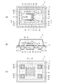
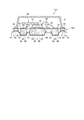
図1は、振動デバイスとしてのセンサーデバイスの一実施形態の概略構成を示す模式図であり、(a)は、半導体回路素子としてのICチップ側(上側)から俯瞰した平面図、(b)は、(a)のA−A線断面図、(c)は、底面側(下側)から俯瞰した平面図である。
図1において、センサーデバイス1は、複数の金属支柱と、それら金属支柱を互いに電気的に独立させた状態で一体に固定する絶縁体33と、を備えた基板2と、基板2に搭載されたICチップ10及び振動片としてのセンサー素子20と、ICチップ10及びセンサー素子20を覆うように設けられた蓋体9と、を有している。
これら複数の金属支柱、即ち、第1の金属支柱3、第2の金属支柱4A,4B,4A´,4B´、第4の金属支柱6A,6B、及び第3の金属支柱5は、互いに電気的に独立するように隙間を介して配置され、各金属支柱間の隙間には、絶縁体33が充填されて固化されている。これにより、筒状の第3の金属支柱5に囲まれて配置された第1の金属支柱3、第2の金属支柱4A,4B,4A´,4B´、及び第4の金属支柱6A,6Bが一体に固定された基板2が形成される。
ここで、一方の一対の第2の金属支柱4A´,4B´及び金属配線部7A,7Bの第2の面2bが、第1の金属支柱3、他方の一対の第2の金属支柱4A,4B、及び第4の金属支柱6A,6Bの第2の面2bよりも第1の面2a側にある。換言すると、一方の一対の第2の金属支柱4A´,4B´及び金属配線部7A,7Bの第1の面2aと第2の面2bとの間の距離は、第1の金属支柱3、他方の一対の第2の金属支柱4A,4B、及び第4の金属支柱6A,6Bの第1の面2aと第2の面2bとの合いだの距離より短い。即ち、第1の金属支柱3、他方の一対の第2の金属支柱4A,4B、及び第4の金属支柱6A,6Bの第2の面2bは、センサーデバイス1を外部基板に実装する際に、外部基板と接触して電気的な接続を図るための実装端子になっており、一方の一対の第2の金属支柱4A´,4B´及び金属配線部7A,7Bは、外部基板に接触しないようになっている。ICチップ10の電極パッド11とボンディングワイヤー99を介して電気的に接続された一方の一対の第2の金属支柱4A´,4B´は、金属配線部7A,7Bを経て電気的に接続された第4の金属支柱6A,6Bの第2の面2b(実装端子)により外部基板との接続を図るようになっている。
このような構成の第3の金属支柱5を有することにより、筒状の第3の金属支柱5内に複数の金属支柱が夫々電気的に独立した態様で絶縁体33により固定された基板2と、その基板2にICチップ10とセンサー素子とを搭載して蓋体9により封止したセンサーデバイス1を提供することができる。また、センサーデバイス1を外部基板に実装する際に電気的な接続には寄与しない第3の金属支柱5の第2の面2bが、外部基板との電気的な接続に供する第1の金属支柱3、第2の金属支柱4A,4B、及び第4の金属支柱6A,6Bの第2の面よりも第1の面2a側にあるため、第3の金属支柱5の第2の面2bが外部基板の配線に接触しないので、短絡するなどの不具合が回避でき、外部基板の配線レイアウトの自由度が増すという効果を奏する。
ICチップ10には、能動面10a側にトランジスターやメモリー素子などの半導体素子を含んで構成される集積回路(図示せず)が形成されている。この集積回路には、例えば、センサー素子20を駆動振動させるための駆動回路と、物理量が加わったときにセンサー素子20に生じる検出振動を検出する検出回路とが備えられている。
ICチップ10は、能動面10a側に設けられた複数の電極パッド11と、センサー素子20の上記外部接続端子と電気的に接続されるマウント電極とを備えている。
また、図示はしないが、ICチップ10の能動面10a上には、パッシベーション膜となる絶縁膜が形成されており、この絶縁膜には、電極パッド11とマウント電極とを外側に露出させる開口部が設けられている。絶縁膜は、酸化珪素(SiO2)、窒化珪素(Si3N4)などの無機絶縁材料や、ポリイミド樹脂、シリコーン変性ポリイミド樹脂、エポキシ樹脂、シリコーン変性エポキシ樹脂、アクリル樹脂、フェノール樹脂、BCB(benzocyclobutene)及びPBO(polybenzoxazole)などの樹脂を用いて形成することができる。
電極パッド11やその他の電極は、チタン(Ti)、窒化チタン(TiN)、アルミニウム(Al)、銅(Cu)、または、これらを含む合金などを用いて形成することができる。特に電極パッド11については、ワイヤーボンディングの際の接合性を高めるため、その表面にニッケル(Ni)、金(Au)のメッキを施しておくのが好ましい。このようにすることで、特にさびによる接触性、接合性の低下を防止することができる。
また、電極パッド11やその他の電極は、ハンダメッキ、ハンダプリコートなどの最表面処理を施したものとしてもよい。
接合部材97は、ICチップ10とセンサー素子20との間に隙間を設けるギャップ材としての厚みを有した導電性の接合部材97であり、例えば、銀(Ag)ペースト等の導電性接着剤や、金(Au)などにより形成されたスタッドバンプを用いることができる。スタッドバンプは、金ワイヤーを用いて放電加熱により金ボールを形成し、超音波を印加させるなどの方法により金ボールをICチップのマウント電極上に接合させることにより形成するものであり、ワイヤー径の小さい金ワイヤーを用いることによって微細なバンプを比較的容易に形成することができる。
水晶を用いて形成されるセンサー素子20は、水晶結晶軸において直交するX軸及びY軸で規定される平面に沿って切り出されて平板状に加工され、平面と直交するZ軸方向に所定の厚みを有している。なお、所定の厚みは、発振周波数(共振周波数)、外形サイズ、加工性などにより適宜設定される。
本実施形態のセンサー素子20は、支持部21と、支持部21から並行させて延出された一対の振動部(振動腕)22,22とを有する所謂音叉型の振動片である。このような形状のセンサー素子20は、フォトリソグラフィー技術を用いたエッチング(ウェットエッチングまたはドライエッチング)により形成されている。なお、センサー素子20は、1枚の水晶ウエハーから複数個取りすることが可能である。
蓋体9は、基板2の筒状の第3の金属支柱5の第1の面2a上にシームリングなどを介したシーム溶接などの接合方法により電気的な接続を図りながら接合されている。これにより、基板2と蓋体9とにより形成される空間が気密に封止される。このとき、ICチップ10及びセンサー素子20が収容された空間が、センサー素子20の振動が阻害されないように、真空状態(真空度が高い状態)あるいは不活性ガス雰囲気に保持されていることが望ましく、蓋体9を接合する封止工程では、前記空間から外部に脱気を行いながら封止したり、あるいは窒素(N2)やアルゴン(Ar)などの不活性ガスを注入して封止したりする。
これにより、従来のセンサーデバイス(振動デバイス)で基板として用いられるセラミック基板やセラミックパッケージに比して、基板に用いる材料が安価であると共に、ICチップやセンサー素子20の設計変更に対して、フォトリソグラフィーのフォトマスクの変更のみで対応することができるので、低コスト化が図られたセンサーデバイス1を提供することができる。
次に、上記第1の実施形態のセンサーデバイス1の製造方法について説明する。
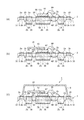
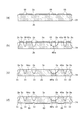
図2は、センサーデバイス1の製造方法を示すフローチャートである。
また、図3及び図4は、センサーデバイス1の製造方法において各工程の態様を模式的に説明する正断面図である。
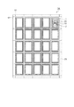
また、図5は、センサーデバイス1の製造方法において金属板シートに複数のセンサーデバイス1が縦横に並べて形成された過程を示す平面図である。
具体的には、まず、第1めっき工程にて、電解めっき法などにより、金属板シート2Aの第1の面全面に第1めっき層35を形成し、第2の面全面に第2めっき層36を形成する。第1めっき層35及び第2めっき層36を同時に形成することができる。
次に、フォトリソグラフィーを利用して第1めっき層35及び第2めっき層36の一部を除去することにより、図3(a)に示すように、複数の金属支柱を形成するためのエッチングマスクパターンとなる第1めっき層35と第2めっき層36とを、第1の面2aまたは第2の面2bに形成する(図2のステップS−1)。
なお、第1めっき層35及び第2めっき層36によるエッチングマスクパターンの形成は、金属板シート2Aの第1の面2a及び第2の面2bの夫々に、フォトリソフラフィーを用いて形成されたフォトレジストによるめっきマスクパターンを形成し、第1めっき層35および第2めっき層を選択的に形成した後にフォトレジストを剥離する方法によっても形成することができる。
なお、図3及び図4の断面では、第2の金属支柱4A,4B´、及び、第4の金属支柱6Aの夫々と対をなす第2の金属支柱4B,4A´、及び、第4の金属支柱6Bが図示されないが、これらの一部となる凸部も同時に形成され、以降の工程でも同時に加工が進められていく(以下、説明は省略する)。
また、この第1エッチング工程では、金属配線部7B、及びそれと対をなす金属配線部7A(図示されず)の一部も同時に形成される。
なお、第1めっき層35が例えばニッケル/パラジウム/金(Ni/Pd/Au)、又は、ニッケル/金(Ni/Au)からなる場合は、上記エッチング液にアルカリ溶液を用いることが好ましい。Niはアルカリ溶液に溶けにくいので、図3(b)に示すように、第1めっき層35は、各凸部3a,4Aa,4B´a,5a,6Aaの表面(第1の面2a)からそれぞれ外側へはみ出すように残って形成される。
なお、本実施形態のように、焼成することにより固化する絶縁体33を用いる場合は、焼成によって金属板シート2Aの物性が劣化しないように、比較的低い焼成温度の絶縁体33材料を用いることが好ましい。
ここで、第3の金属支柱5と、金属配線部7Bとの第2の面2bには第2めっき層36によるエッチングマスクパターンは形成されていないので、第3の金属支柱5、及び金属配線部7Bの第2の面2bは、上記したように、他の金属支柱の第2の面2bよりも第1の面2a側までエッチングされる。
これにより、図5に示すように、金属板シート2Aに平面視で縦横等間隔に並んで連結された複数のセンサーデバイス1が形成される。
次に、センサーデバイス1の外観的特性や電気的特性を検査する特性検査を行って、各特性が規格内に入っている良品と、規格外となる不良品とを選別して(図2のステップS11)、一連のセンサーデバイス1の製造を終了する。
このように、ICチップ10の電極パッド11と電気的に接続される第2の金属支柱4A´,4B´を、金属配線部7A,7Bを介して、外部基板との接続を図る第4の金属支柱6A,6Bに再配置する再配置配線を形成することにより、ICチップ10の電極パッドの配置の変更や外部基板の設計変更に対して比較的容易に対応することができる。これにより、複数の前記金属支柱は第4の金属支柱を含み、前記第2の金属支柱と前記第4の支柱とを電気的に接続する金属配線部を有し、前記金属配線部の前記第2の面が、前記第1の金属支柱、前記第2の金属支柱、及び前記第4の金属支柱の前記第2の面よりも前記第1の面側にあることを特徴とする。
これによれば、第1エッチング工程及び第2エッチング工程においてエッチングマスクとして利用した第1めっき層35及び第2めっき層36を、各金属支柱において、ICチップ10及びセンサー素子20、あるいは外部基板との電気的な接続を図る際の接点金属としてそのまま利用できるので、センサーデバイス1の低コスト化に顕著な効果を奏する。
これにより、ICチップ10やセンサー素子20を覆うように接合される蓋体9がシールド効果を奏して、外部の電磁波の影響によりICチップ10が誤動作したり、ICチップ10の不要な電磁波が外部に悪影響を及ぼしたりする不具合を回避することができる。
これにより、製造効率が向上して製造コストを顕著に低減することができる。
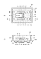
以下、センサーデバイスの第2の実施形態について説明する。
図6は、センサーデバイスの第2の実施形態の概略構成を示す模式図であり、図1における図1(b)と同じ断面を示す断面図である。
なお、第2の実施形態のセンサーデバイスは、基板の第1の面及び第2の面に形成されるめっき層以外の構成は、上記第1の実施形態のセンサーデバイス1と同じであるため、上記第1の実施形態との共通部分については同一符号を付して説明を省略する。
金属板を加工することにより形成された基板102は、上記第1の実施形態のセンサーデバイス1の基板2(図1、図3、図4を参照)と概ね同じ構成を有している。即ち、基板102は、第1の金属支柱3、二対の第2の金属支柱4A,4B´、第4の金属支柱6A、及び、第2の金属支柱4B´と第4の金属支柱6Aとを夫々電気的に接続する金属配線部7B、これらの金属支柱及び金属配線部を平面視で囲むように配置された筒状の第3の金属支柱5が、絶縁体33によって一体に固定されて形成されている。
これによれば、基板102の金属板の露出面の全てに第1めっき層85または第2めっき層が形成されているので、金属板の金属面が露出された場合に比して耐蝕性が向上する。
また、例えば、半田接合によりセンサーデバイス101を外部基板に実装する際に、半田などの接合部材が各金属支柱の第2の面2bだけでなく側面にまで濡れ広がって良好なフィレットを形成することができる。
したがって、接続信頼性の高いセンサーデバイス101を提供することができる。
図7は、第2の実施形態のセンサーデバイスの製造方法を示すフローチャートである。
また、図8及び図9は、第2の実施形態のセンサーデバイスの製造方法において各工程での態様を模式的に説明する正断面図である。
なお、本実施形態のセンサーデバイス101は、基板102以外の構成は上記第1の実施形態のセンサーデバイス1と同じであるため、上記実施形態と同じ工程については同一符号を付して説明を省略する。また、図7及び図8には基板の製造過程のみを示す。
次に、図8(c)に示すように、第1エッチング工程で凸部3a,4Aa,4B´a,5a,6Aaの形成に伴って形成される凹部に、絶縁体33を充填して固化させる絶縁体形成を行う(図2のステップS23)。
ここまでの工程により、金属板シート2Aに平面視で並んで連結された複数の基板102が形成される(図7のステップS26)。
以下、センサーデバイスの変形例について図面を参照して説明する。
図10は、センサーデバイスの変形例の概略構成を示す模式図であり、(a)は、ICチップ側(上側)から俯瞰した平面図、(b)は、(a)のB−B線断面図である。なお、上記実施形態との共通部分については同一符号を付して説明を省略し、上記実施形態と異なる構成を中心に説明する。
金属板を加工することにより形成された基板202は、上記第1の実施形態のセンサーデバイス1の基板2(図1、図3、図4を参照)と概ね同じ構成の複数の金属支柱を有している。即ち、基板202は、第1の金属支柱3、二対の第2の金属支柱4A,4B,4A´,4B´、第4の金属支柱6A,6B、及び、第2の金属支柱4A´,4B´と第4の金属支柱6A,6Bとを夫々電気的に接続する金属配線部7A,7B、これらの金属支柱及び金属配線部を平面視で囲むように配置された筒状の第3の金属支柱205が、絶縁体33によって一体に固定されて形成されている。
このような構成の基板202を形成するには、まず、上記実施形態で述べたセンサーデバイスの製造方法の基板の製造工程において(図2、図3を参照)、第1エッチング工程で金属支柱の第1の面2a側の一部(凸部)を形成する前に、第3の金属支柱205の第1の面202aとなる領域をマスクして金属板をハーフエッチングすることによって、第3の金属支柱205の上方の筒状の壁を形成する。その後で、上記実施形態のセンサーデバイスの製造方法に沿って基板202を形成し、その基板202上に上記第1の実施形態と同じ態様でICチップ10及びセンサー素子20を搭載する。そして、第3の金属支柱205の第1の面202aに平板状の蓋体209を接合してICチップ10及びセンサー素子を封止することにより、本変形例のセンサーデバイス201を製造することができる。
また、第3の金属支柱205によりICチップ10やセンサー素子20が囲まれることにより、第3の金属支柱205がシールド効果を奏して電磁波を遮蔽することができるので、外部の電磁波の影響によるICチップなどの誤動作や、ICチップ10の不要な電磁波が外部に及ぼす悪影響を回避することができる。
なお、この構成において、蓋体209に金属を用いるか、または金属層を有する構成とすることによって、シールド効果をより顕著に得ることができる。
〔電子機器〕
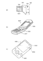
上記実施形態及び変形例に記載のセンサーデバイスを搭載した電子機器は、低コスト化及び信頼性の向上が可能である。
例えば、図11(a)は、デジタルビデオカメラへの適用例を示す。デジタルビデオカメラ240は、受像部241、操作部242、音声入力部243、及び表示ユニット1001を備えている。このようなデジタルビデオカメラ240に、上記実施形態のセンサーデバイス1を備えたセンサーを搭載することにより、所謂手ぶれ補正機能を搭載することができる。
また、図11(b)は、電子機器としての携帯電話機、図11(c)は、情報携帯端末(PDA:Personal Digital Assistants)への適用例をそれぞれ示すものである。
まず、図11(b)に示す携帯電話機3000は、複数の操作ボタン3001及びスクロールボタン3002、並びに表示ユニットと1002を備える。スクロールボタン3002を操作することによって、表示ユニット1002に表示される画面がスクロールされる。
また、図11(c)に示すPDA4000は、複数の操作ボタン4001及び電源スイッチ4002、並びに表示ユニット1003を備える。電源スイッチ4002を操作すると、住所録やスケジュール帳といった各種の情報が表示ユニット1003に表示される。
このような携帯電話機3000やPDA4000に、上記実施形態のセンサーデバイスを搭載することにより、様々な機能を付与することができる。例えば、図11(b)の携帯電話機3000に、図示しないカメラ機能を付与した場合に、携帯電話機3000に搭載されるセンサーデバイスとしてジャイロセンサーを用いることにより、手振れ補正を行うことができる。また、図11(b)の携帯電話機3000や、図11(c)のPDA4000にGPS(Global Positioning System)として広く知られる汎地球測位システムを具備した場合に、上記実施形態のセンサーデバイスを搭載することにより、GPSにおいて、携帯電話機3000やPDA4000の位置や姿勢を認識させることができる。
これらの電子機器は、上記実施形態および変形例のセンサーデバイスを用いているので、低コスト化、及び、信頼性の向上を図ることが可能である。
これに限らず、例えば、ICチップ10の集積回路のデーター書き込みが可能な回路素子から引き出された電極パッド11と、第2の金属支柱とを導電性部材(ボンディングワイヤー99)により接続し、この第2の金属支柱と金属配線部により接続された第4の金属支柱を、ユーザー用の書き込み端子として利用することができる。このとき、第4の金属支柱の第2の面を書き込み端子として利用することに限らず、例えば、複数の金属支柱を取り囲むように配置された第3の金属支柱の一部をエッチング加工及び絶縁体による固定によって電気的に独立させ、この第3の金属支柱の一部、即ちセンサーデバイスの側面にユーザー用の書き込み端子を配置して提供することもできる。
これに限らず、第1エッチングには第1の実施形態と同様に第1めっき層35をエッチングマスクとして利用して、第2エッチング後には金属板の第2の面2b側のみに無電解めっき法による第2めっき層を形成する構成としてもよい。
また、圧電体材料以外の材料を用いて振動片を形成することができる。例えば、シリコン半導体材料などを用いて振動素子を形成することもできる。
また、振動素子の駆動振動の励振方式や検出振動の検出方式は、圧電効果によるものだけに限らない。静電気力(クーロン力)を用いた静電駆動型や、磁力を利用したローレンツ駆動型などの振動片においても、本発明の構成及びその効果を発揮させることができる。
したがって、本発明のセンサーデバイスを利用したセンサーは、角速度を検出するジャイロセンサーや、角加速度、加速度、力、温度、磁気など、種々の物理量を検出するセンサーとして利用することができる。
Claims (16)
- 第1の面及び前記第1の面とは反対側の第2の面を有し、複数の金属支柱であって第1の金属支柱及び第2の金属支柱を含む前記金属支柱と、複数の前記金属支柱の前記第1の面及び前記第2の面とは異なる面の隙間に充填され複数の前記金属支柱を一体に固定する絶縁体と、を備えた基板と、
第3の面に電極を有し、前記第3の面とは反対側の第4の面を前記第1の金属支柱の前記第1の面に対向させて前記第1の金属支柱に固定された半導体回路素子と、
支持部と、前記支持部から延出された振動部とを有し、前記支持部を前記半導体回路素子の前記第3の面に接合することにより前記半導体回路素子に支持された振動片と、
前記電極と前記第2の金属支柱とを電気的に接続する導電性部材と、
前記半導体回路素子及び前記振動片を覆うように設けられた蓋体と、
を有することを特徴とする振動デバイス。 - 請求項1に記載の振動デバイスにおいて、
複数の前記金属支柱は、前記第1の金属支柱及び前記第2の金属支柱を平面視で囲むように配置された筒状の第3の金属支柱を含み、
前記絶縁体が前記第3の金属支柱の内壁面側に充填され、
前記蓋体が前記第3の金属支柱の前記第1の面に接合され、
前記第3の金属支柱の前記第1の面と前記第2の面との間の距離は、前記第1の金属支柱及び前記第2の金属支柱の前記第1の面と前記第2の面との間の距離より短いことを特徴とする振動デバイス。 - 請求項1または2に記載の振動デバイスにおいて、
複数の前記金属支柱は第4の金属支柱及び金属配線部を含み、
前記金属配線部は前記第2の金属支柱と前記第4の支柱とを電気的に接続し、
前記金属配線部の前記第1の面と前記第2の面との間の距離は、前記第1の金属支柱、前記第2の金属支柱、及び前記第4の金属支柱の前記第1の面と前記第2の面との間の距離より短いことを特徴とする振動デバイス。 - 請求項1〜3のいずれか一項に記載の振動デバイスにおいて、
複数の前記金属支柱の前記第1の面に第1のめっき層を備え、前記第1のめっき層は前記第1の面から外側へはみ出していることを特徴とする振動デバイス。 - 請求項1〜4のいずれか一項に記載の振動デバイスにおいて、
前記金属支柱の前記第2の面、及び、前記第2の面側の前記第2の面とは異なる面に第2のめっき層を備えていることを特徴とする振動デバイス。 - 請求項2に記載の振動デバイスにおいて、
前記第3の金属支柱の前記第1の面が、他の前記金属支柱の前記第1の面よりも高い位置にあることを特徴とする振動デバイス。 - 請求項6に記載の振動デバイスにおいて、
前記第3の金属支柱の前記第1の面が、前記振動片よりも高い位置にあることを特徴とする振動デバイス。 - 請求項1〜7のいずれか一項に記載の振動デバイスにおいて、
前記蓋体は金属部分を含み、前記蓋体と前記第3の金属支柱とが電気的に接続されていることを特徴とする振動デバイス。 - 第1の面及び前記第1の面とは反対側の第2の面を有する金属板を前記第1の面から部分的にエッチングして複数の凸部を形成する第1エッチング工程と、
前記第1エッチング工程で前記凸部の形成に伴って形成される凹部に絶縁体を充填して固着させる絶縁体形成工程と、
前記絶縁体形成工程の後で、前記金属板を前記第2の面から前記凹部と連通するように部分的にエッチングすることにより、前記凸部から前記第2の面に延びる金属支柱であって、第1の金属支柱及び第2の金属支柱を含む複数の前記金属支柱を形成する第2エッチング工程と、
前記第1の金属支柱の前記第1の面に、第3の面に電極を有する半導体回路素子の前記第3の面とは反対側の第4の面を対向させて接合する半導体回路素子接合工程と、
前記半導体回路素子の前記第3の面に振動片を固定する振動片固定工程と、
前記電極と前記第2の金属支柱とを導電性部材により電気的に接続するボンディング工程と、
前記半導体回路素子及び前記振動片を覆うように蓋体を設ける封止工程と、
を含むことを特徴とする振動デバイスの製造方法。 - 請求項9に記載の振動デバイスの製造方法において、
前記第1エッチング工程の前に前記第1の面に第1のめっき層を形成する第1めっき工程を含み、
前記第1エッチング工程では、前記第1めっき層をエッチングマスクとして利用することを特徴とする振動デバイスの製造方法。 - 請求項9または10に記載の振動デバイスの製造方法において、
前記第2エッチング工程の後に、無電解めっき法による第2めっき工程を有することを特徴とする振動デバイスの製造方法。 - 請求項9に記載の振動デバイスの製造方法において、
前記第2エッチング工程の後に、無電解めっき法により前記第1の面の前記第1めっき層及び前記第2の面の前記第2めっき層を同時に形成するめっき工程を有することを特徴とする振動デバイスの製造方法。 - 請求項9〜12のいずれか一項に記載の振動デバイスの製造方法において、
前記第1のエッチング工程及び前記第2のエッチング工程により、前記第1の金属支柱及び前記第2の金属支柱を平面視で囲むように配置され前記第2の面が前記第1の金属支柱及び前記第2の金属支柱の前記第2の面よりも前記第1の面側にある筒状の第3の金属支柱を形成し、
前記絶縁体形成工程では、前記絶縁体を前記第3の金属支柱の内壁面側に充填し、
前記封止工程では、前記蓋体を前記第3の金属支柱の前記第1の面に接合することを特徴とする振動デバイスの製造方法。 - 請求項13に記載の振動デバイスの製造方法において、
前記第1のエッチング工程の前に、
前記第3の金属支柱の前記第1の面となる領域をマスクして前記金属板を前記第1の面から所定量エッチングする工程を含むことを特徴とする振動デバイスの製造方法。 - 請求項9〜14のいずれか一項に記載の振動デバイスの製造方法において、
前記第1エッチング工程、前記絶縁体形成工程、及び前記第2エッチング工程では、複数の前記金属支柱を有する一個片の基板を一つの前記金属板に平面視で複数個並べて形成し、
前記半導体回路素子接合工程では、複数個の前記回路素子を、前記複数個の前記基板の夫々に平面視で並べて接合し、
前記振動片接続工程では、複数個の前記振動片を、前記複数個の半導体回路素子夫々の上に並べて接続し、
前記ボンディング工程では、前記複数個の半導体回路素子の前記電極と前記複数個の基板の前記第2の金属支柱とを前記導電性部材で夫々接続し、
前記封止工程では、前記複数個の基板ごとに接合された前記半導体回路素子及び前記振動片を複数の前記蓋体で一括して封止して、前記金属板に連結された複数の振動デバイスを形成し、
前記封止工程の後で、前記連結された複数の振動デバイスを個片に切り出すダイシング工程を有することを特徴とする振動デバイスの製造方法。 - 請求項1〜8のいずれか一項に記載の振動デバイス、または、請求項9〜14のいずれか一項に記載された製造方法により製造された振動デバイスを備えていることを特徴とする電子機器。
Priority Applications (3)
| Application Number | Priority Date | Filing Date | Title |
|---|---|---|---|
| JP2011045999A JP5678727B2 (ja) | 2011-03-03 | 2011-03-03 | 振動デバイス、振動デバイスの製造方法、電子機器 |
| US13/401,443 US9088262B2 (en) | 2011-03-03 | 2012-02-21 | Vibrating device, method for manufacturing vibrating device, and electronic apparatus |
| CN201210052291XA CN102655143A (zh) | 2011-03-03 | 2012-03-01 | 振动装置、振动装置的制造方法以及电子设备 |
Applications Claiming Priority (1)
| Application Number | Priority Date | Filing Date | Title |
|---|---|---|---|
| JP2011045999A JP5678727B2 (ja) | 2011-03-03 | 2011-03-03 | 振動デバイス、振動デバイスの製造方法、電子機器 |
Publications (2)
| Publication Number | Publication Date |
|---|---|
| JP2012182765A true JP2012182765A (ja) | 2012-09-20 |
| JP5678727B2 JP5678727B2 (ja) | 2015-03-04 |
Family
ID=46730741
Family Applications (1)
| Application Number | Title | Priority Date | Filing Date |
|---|---|---|---|
| JP2011045999A Expired - Fee Related JP5678727B2 (ja) | 2011-03-03 | 2011-03-03 | 振動デバイス、振動デバイスの製造方法、電子機器 |
Country Status (3)
| Country | Link |
|---|---|
| US (1) | US9088262B2 (ja) |
| JP (1) | JP5678727B2 (ja) |
| CN (1) | CN102655143A (ja) |
Cited By (3)
| Publication number | Priority date | Publication date | Assignee | Title |
|---|---|---|---|---|
| US9444466B2 (en) | 2014-03-27 | 2016-09-13 | Seiko Epson Corporation | Method of adjusting frequency of resonation device and method of manufacturing resonation device |
| US9954160B2 (en) | 2013-11-12 | 2018-04-24 | Seiko Epson Corporation | Wiring board, method of manufacturing the same, element housing package, electronic device, electronic apparatus, and moving object |
| JP7408886B2 (ja) | 2020-03-31 | 2024-01-09 | 長華科技股▲ふん▼有限公司 | 半導体素子搭載用基板 |
Families Citing this family (16)
| Publication number | Priority date | Publication date | Assignee | Title |
|---|---|---|---|---|
| JP6010968B2 (ja) * | 2012-03-29 | 2016-10-19 | セイコーエプソン株式会社 | 振動デバイス及び振動デバイスの製造方法 |
| JP6136349B2 (ja) * | 2013-02-22 | 2017-05-31 | セイコーエプソン株式会社 | 電子デバイス、電子機器及び移動体 |
| US9659855B2 (en) | 2013-08-27 | 2017-05-23 | Ubotic Company Limited | Cavity package with pre-molded substrate |
| US9257370B2 (en) | 2013-08-27 | 2016-02-09 | Ubotic Company Limited | Cavity package with pre-molded cavity leadframe |
| JP6357758B2 (ja) * | 2013-11-25 | 2018-07-18 | セイコーエプソン株式会社 | 物理量センサー、電子機器および移動体 |
| CN103812470B (zh) * | 2014-02-22 | 2016-07-06 | 烟台明德亨电子科技有限公司 | 一种簧片、石英晶体谐振器及加工方法 |
| JP6017492B2 (ja) * | 2014-04-24 | 2016-11-02 | Towa株式会社 | 樹脂封止電子部品の製造方法、突起電極付き板状部材、及び樹脂封止電子部品 |
| JP6508217B2 (ja) * | 2015-01-16 | 2019-05-08 | 株式会社村田製作所 | 基板、基板の製造方法及び弾性波装置 |
| US9887687B2 (en) * | 2015-01-28 | 2018-02-06 | Analog Devices Global | Method of trimming a component and a component trimmed by such a method |
| CN107924877B (zh) * | 2015-08-11 | 2020-08-28 | 株式会社村田制作所 | 高频模块及其制造方法 |
| CN108463928B (zh) * | 2016-01-30 | 2020-07-14 | 伊雷克托科学工业股份有限公司 | 系统隔离和光学隔间密封 |
| JP6724502B2 (ja) * | 2016-04-06 | 2020-07-15 | セイコーエプソン株式会社 | 超音波装置 |
| JP7102113B2 (ja) * | 2017-09-11 | 2022-07-19 | ファスフォードテクノロジ株式会社 | ダイボンディング装置および半導体装置の製造方法 |
| KR101999594B1 (ko) * | 2018-02-23 | 2019-10-01 | 해성디에스 주식회사 | 반도체 패키지 기판 제조방법, 이를 이용하여 제조된 반도체 패키지 기판, 반도체 패키지 제조방법 및 이를 이용하여 제조된 반도체 패키지 |
| JP2022043369A (ja) * | 2018-12-26 | 2022-03-16 | ソニーセミコンダクタソリューションズ株式会社 | 半導体装置および電子機器 |
| CN112701211B (zh) * | 2020-12-29 | 2023-04-28 | 上海烨映微电子科技股份有限公司 | 红外热电堆封装结构及方法 |
Citations (2)
| Publication number | Priority date | Publication date | Assignee | Title |
|---|---|---|---|---|
| JPH0738334A (ja) * | 1993-07-22 | 1995-02-07 | Seikosha Co Ltd | 水晶発振器 |
| WO2010035499A1 (ja) * | 2008-09-29 | 2010-04-01 | 凸版印刷株式会社 | リードフレーム基板とその製造方法ならびに半導体装置 |
Family Cites Families (16)
| Publication number | Priority date | Publication date | Assignee | Title |
|---|---|---|---|---|
| US4520413A (en) * | 1982-04-13 | 1985-05-28 | Minnesota Mining And Manufacturing Company | Integrated magnetostrictive-piezoelectric-metal oxide semiconductor magnetic playback head |
| JP3018542B2 (ja) * | 1991-04-03 | 2000-03-13 | セイコーエプソン株式会社 | リードフレーム及びその製造方法 |
| JP3235606B2 (ja) | 1999-11-01 | 2001-12-04 | セイコーエプソン株式会社 | リードフレーム及びその製造方法、並びに半導体装置 |
| JP2002118423A (ja) | 2000-10-06 | 2002-04-19 | Seiko Epson Corp | 圧電デバイス及びその製造方法 |
| JP2005292079A (ja) | 2004-04-05 | 2005-10-20 | Seiko Epson Corp | 圧電デバイス、及び圧電発振器 |
| US7157836B2 (en) * | 2004-10-19 | 2007-01-02 | Seiko Epson Corporation | Piezoelectric device |
| JP4638800B2 (ja) * | 2005-10-27 | 2011-02-23 | 株式会社日立ハイテクノロジーズ | 走査電子顕微鏡装置における機差管理システムおよびその方法 |
| JP4270282B2 (ja) | 2007-01-23 | 2009-05-27 | セイコーエプソン株式会社 | 半導体装置の製造方法 |
| US7807498B2 (en) | 2007-07-31 | 2010-10-05 | Seiko Epson Corporation | Substrate, substrate fabrication, semiconductor device, and semiconductor device fabrication |
| JP5131206B2 (ja) | 2009-01-13 | 2013-01-30 | セイコーエプソン株式会社 | 半導体装置 |
| JP5278166B2 (ja) | 2009-05-28 | 2013-09-04 | セイコーエプソン株式会社 | 電子デバイスの製造方法及び電子デバイス |
| JP2011139024A (ja) * | 2009-12-04 | 2011-07-14 | Seiko Epson Corp | パッケージ、および、それを用いた振動デバイス |
| JP2011133299A (ja) | 2009-12-24 | 2011-07-07 | Seiko Epson Corp | センサーデバイス、センサーデバイスの製造方法、モーションセンサー及びモーションセンサーの製造方法 |
| JP2011149789A (ja) | 2010-01-21 | 2011-08-04 | Seiko Epson Corp | モーションセンサーの製造方法、およびモーションセンサー |
| US8502363B2 (en) * | 2011-07-06 | 2013-08-06 | Advanced Semiconductor Engineering, Inc. | Semiconductor device packages with solder joint enhancement element and related methods |
| US8674487B2 (en) * | 2012-03-15 | 2014-03-18 | Advanced Semiconductor Engineering, Inc. | Semiconductor packages with lead extensions and related methods |
-
2011
- 2011-03-03 JP JP2011045999A patent/JP5678727B2/ja not_active Expired - Fee Related
-
2012
- 2012-02-21 US US13/401,443 patent/US9088262B2/en not_active Expired - Fee Related
- 2012-03-01 CN CN201210052291XA patent/CN102655143A/zh active Pending
Patent Citations (2)
| Publication number | Priority date | Publication date | Assignee | Title |
|---|---|---|---|---|
| JPH0738334A (ja) * | 1993-07-22 | 1995-02-07 | Seikosha Co Ltd | 水晶発振器 |
| WO2010035499A1 (ja) * | 2008-09-29 | 2010-04-01 | 凸版印刷株式会社 | リードフレーム基板とその製造方法ならびに半導体装置 |
Cited By (3)
| Publication number | Priority date | Publication date | Assignee | Title |
|---|---|---|---|---|
| US9954160B2 (en) | 2013-11-12 | 2018-04-24 | Seiko Epson Corporation | Wiring board, method of manufacturing the same, element housing package, electronic device, electronic apparatus, and moving object |
| US9444466B2 (en) | 2014-03-27 | 2016-09-13 | Seiko Epson Corporation | Method of adjusting frequency of resonation device and method of manufacturing resonation device |
| JP7408886B2 (ja) | 2020-03-31 | 2024-01-09 | 長華科技股▲ふん▼有限公司 | 半導体素子搭載用基板 |
Also Published As
| Publication number | Publication date |
|---|---|
| US20120223622A1 (en) | 2012-09-06 |
| JP5678727B2 (ja) | 2015-03-04 |
| CN102655143A (zh) | 2012-09-05 |
| US9088262B2 (en) | 2015-07-21 |
Similar Documents
| Publication | Publication Date | Title |
|---|---|---|
| JP5678727B2 (ja) | 振動デバイス、振動デバイスの製造方法、電子機器 | |
| JP5838543B2 (ja) | センサーデバイス、モーションセンサー、および電子機器 | |
| JP5737848B2 (ja) | センサーデバイス、センサーデバイスの製造方法、モーションセンサー及びモーションセンサーの製造方法 | |
| JP5970698B2 (ja) | 振動片、センサーユニット、電子機器 | |
| JP2006279872A (ja) | 圧電振動子及びその製造方法並びにその圧電振動子を用いた圧電発振器の製造方法 | |
| JP2012193971A (ja) | センサーモジュール、センサーデバイス、センサーデバイスの製造方法及び電子機器 | |
| JP2013002938A (ja) | センサーデバイス、およびその製造方法 | |
| US8669819B2 (en) | Electronic component package sealing member, electronic component package, and method for manufacturing electronic component package sealing member | |
| JP5682361B2 (ja) | 振動デバイス、振動デバイスの製造方法、モーションセンサー、および電子機器 | |
| JP5987426B2 (ja) | 振動片、振動片の製造方法、センサーユニット、電子機器 | |
| JP2013046167A (ja) | 振動デバイス、及び振動デバイスの製造方法 | |
| US7876168B2 (en) | Piezoelectric oscillator and method for manufacturing the same | |
| JP5030135B2 (ja) | 圧電単結晶振動子および圧電振動ジャイロ | |
| JP5440148B2 (ja) | 圧電デバイスの製造方法 | |
| JP5716557B2 (ja) | 振動片、ジャイロセンサー、電子機器、振動片の製造方法 | |
| JP2013046168A (ja) | 振動デバイスの製造方法 | |
| JP2009232449A (ja) | 圧電振動子及び発振器 | |
| JP5838694B2 (ja) | 物理量検出器、物理量検出デバイス及び電子機器 | |
| JP2011117859A (ja) | 物理量検出装置 | |
| JP2005241380A (ja) | 圧電デバイスならびに圧電デバイスを利用した携帯電話装置および圧電デバイスを利用した電子機器 | |
| JP2012167941A (ja) | センサーデバイス、モーションセンサー、電子機器 | |
| JP2008003017A (ja) | 圧電単結晶振動子および圧電振動ジャイロ | |
| JP2011182306A (ja) | 圧電デバイスおよびその製造方法 | |
| JP2007142947A (ja) | 表面実装型圧電発振器 | |
| JP6187658B2 (ja) | センサーデバイス及びセンサー |
Legal Events
| Date | Code | Title | Description |
|---|---|---|---|
| A621 | Written request for application examination |
Free format text: JAPANESE INTERMEDIATE CODE: A621 Effective date: 20131213 |
|
| A977 | Report on retrieval |
Free format text: JAPANESE INTERMEDIATE CODE: A971007 Effective date: 20140718 |
|
| A131 | Notification of reasons for refusal |
Free format text: JAPANESE INTERMEDIATE CODE: A131 Effective date: 20140729 |
|
| A521 | Request for written amendment filed |
Free format text: JAPANESE INTERMEDIATE CODE: A523 Effective date: 20140924 |
|
| TRDD | Decision of grant or rejection written | ||
| A01 | Written decision to grant a patent or to grant a registration (utility model) |
Free format text: JAPANESE INTERMEDIATE CODE: A01 Effective date: 20141209 |
|
| A61 | First payment of annual fees (during grant procedure) |
Free format text: JAPANESE INTERMEDIATE CODE: A61 Effective date: 20141222 |
|
| R150 | Certificate of patent or registration of utility model |
Ref document number: 5678727 Country of ref document: JP Free format text: JAPANESE INTERMEDIATE CODE: R150 |
|
| S531 | Written request for registration of change of domicile |
Free format text: JAPANESE INTERMEDIATE CODE: R313531 |
|
| R350 | Written notification of registration of transfer |
Free format text: JAPANESE INTERMEDIATE CODE: R350 |
|
| LAPS | Cancellation because of no payment of annual fees |