JP2012156362A - 伝送線路、集積回路搭載装置および通信機モジュール - Google Patents
伝送線路、集積回路搭載装置および通信機モジュール Download PDFInfo
- Publication number
- JP2012156362A JP2012156362A JP2011015215A JP2011015215A JP2012156362A JP 2012156362 A JP2012156362 A JP 2012156362A JP 2011015215 A JP2011015215 A JP 2011015215A JP 2011015215 A JP2011015215 A JP 2011015215A JP 2012156362 A JP2012156362 A JP 2012156362A
- Authority
- JP
- Japan
- Prior art keywords
- line
- lines
- integrated circuit
- tapered
- parallel
- Prior art date
- Legal status (The legal status is an assumption and is not a legal conclusion. Google has not performed a legal analysis and makes no representation as to the accuracy of the status listed.)
- Pending
Links
Images


Classifications
-
- H—ELECTRICITY
- H01—ELECTRIC ELEMENTS
- H01P—WAVEGUIDES; RESONATORS, LINES, OR OTHER DEVICES OF THE WAVEGUIDE TYPE
- H01P5/00—Coupling devices of the waveguide type
- H01P5/02—Coupling devices of the waveguide type with invariable factor of coupling
-
- H—ELECTRICITY
- H01—ELECTRIC ELEMENTS
- H01P—WAVEGUIDES; RESONATORS, LINES, OR OTHER DEVICES OF THE WAVEGUIDE TYPE
- H01P5/00—Coupling devices of the waveguide type
- H01P5/12—Coupling devices having more than two ports
-
- H—ELECTRICITY
- H01—ELECTRIC ELEMENTS
- H01L—SEMICONDUCTOR DEVICES NOT COVERED BY CLASS H10
- H01L23/00—Details of semiconductor or other solid state devices
- H01L23/58—Structural electrical arrangements for semiconductor devices not otherwise provided for, e.g. in combination with batteries
- H01L23/64—Impedance arrangements
- H01L23/66—High-frequency adaptations
-
- H—ELECTRICITY
- H01—ELECTRIC ELEMENTS
- H01P—WAVEGUIDES; RESONATORS, LINES, OR OTHER DEVICES OF THE WAVEGUIDE TYPE
- H01P3/00—Waveguides; Transmission lines of the waveguide type
- H01P3/02—Waveguides; Transmission lines of the waveguide type with two longitudinal conductors
- H01P3/08—Microstrips; Strip lines
-
- H—ELECTRICITY
- H03—ELECTRONIC CIRCUITRY
- H03F—AMPLIFIERS
- H03F3/00—Amplifiers with only discharge tubes or only semiconductor devices as amplifying elements
- H03F3/60—Amplifiers in which coupling networks have distributed constants, e.g. with waveguide resonators
- H03F3/602—Combinations of several amplifiers
-
- H—ELECTRICITY
- H03—ELECTRONIC CIRCUITRY
- H03H—IMPEDANCE NETWORKS, e.g. RESONANT CIRCUITS; RESONATORS
- H03H7/00—Multiple-port networks comprising only passive electrical elements as network components
- H03H7/38—Impedance-matching networks
-
- H—ELECTRICITY
- H04—ELECTRIC COMMUNICATION TECHNIQUE
- H04B—TRANSMISSION
- H04B1/00—Details of transmission systems, not covered by a single one of groups H04B3/00 - H04B13/00; Details of transmission systems not characterised by the medium used for transmission
-
- H—ELECTRICITY
- H01—ELECTRIC ELEMENTS
- H01L—SEMICONDUCTOR DEVICES NOT COVERED BY CLASS H10
- H01L2223/00—Details relating to semiconductor or other solid state devices covered by the group H01L23/00
- H01L2223/58—Structural electrical arrangements for semiconductor devices not otherwise provided for
- H01L2223/64—Impedance arrangements
- H01L2223/66—High-frequency adaptations
- H01L2223/6605—High-frequency electrical connections
- H01L2223/6627—Waveguides, e.g. microstrip line, strip line, coplanar line
-
- H—ELECTRICITY
- H01—ELECTRIC ELEMENTS
- H01L—SEMICONDUCTOR DEVICES NOT COVERED BY CLASS H10
- H01L2223/00—Details relating to semiconductor or other solid state devices covered by the group H01L23/00
- H01L2223/58—Structural electrical arrangements for semiconductor devices not otherwise provided for
- H01L2223/64—Impedance arrangements
- H01L2223/66—High-frequency adaptations
- H01L2223/6644—Packaging aspects of high-frequency amplifiers
- H01L2223/6655—Matching arrangements, e.g. arrangement of inductive and capacitive components
-
- H—ELECTRICITY
- H01—ELECTRIC ELEMENTS
- H01L—SEMICONDUCTOR DEVICES NOT COVERED BY CLASS H10
- H01L2224/00—Indexing scheme for arrangements for connecting or disconnecting semiconductor or solid-state bodies and methods related thereto as covered by H01L24/00
- H01L2224/01—Means for bonding being attached to, or being formed on, the surface to be connected, e.g. chip-to-package, die-attach, "first-level" interconnects; Manufacturing methods related thereto
- H01L2224/42—Wire connectors; Manufacturing methods related thereto
- H01L2224/47—Structure, shape, material or disposition of the wire connectors after the connecting process
- H01L2224/49—Structure, shape, material or disposition of the wire connectors after the connecting process of a plurality of wire connectors
- H01L2224/491—Disposition
- H01L2224/4912—Layout
- H01L2224/49175—Parallel arrangements
-
- H—ELECTRICITY
- H01—ELECTRIC ELEMENTS
- H01L—SEMICONDUCTOR DEVICES NOT COVERED BY CLASS H10
- H01L2924/00—Indexing scheme for arrangements or methods for connecting or disconnecting semiconductor or solid-state bodies as covered by H01L24/00
- H01L2924/30—Technical effects
- H01L2924/301—Electrical effects
- H01L2924/30107—Inductance
-
- H—ELECTRICITY
- H01—ELECTRIC ELEMENTS
- H01L—SEMICONDUCTOR DEVICES NOT COVERED BY CLASS H10
- H01L2924/00—Indexing scheme for arrangements or methods for connecting or disconnecting semiconductor or solid-state bodies as covered by H01L24/00
- H01L2924/30—Technical effects
- H01L2924/301—Electrical effects
- H01L2924/3011—Impedance
- H01L2924/30111—Impedance matching
Landscapes
- Engineering & Computer Science (AREA)
- Power Engineering (AREA)
- Physics & Mathematics (AREA)
- Condensed Matter Physics & Semiconductors (AREA)
- General Physics & Mathematics (AREA)
- Computer Hardware Design (AREA)
- Microelectronics & Electronic Packaging (AREA)
- Computer Networks & Wireless Communication (AREA)
- Signal Processing (AREA)
- Microwave Amplifiers (AREA)
- Amplifiers (AREA)
Abstract
【解決手段】テーパー状の平面形状を有する並列に配置された2本のテーパー線路32AA,32AB;32BA,32BBと、2本のテーパー線路の幅の狭い側に対向して設けられた対向線路34A,34Bと、2本のテーパー線路の幅の狭い側と、前記対向線路を接続するワイヤボンディング38AA,38AB;38BA,38BBと、を有し、並列に配置された2本のテーパー線路の幅の狭い側の2つの外側のエッジ間の幅は、2本のテーパー線路の幅の狭い側に対向する対向線路の対向側の外側のエッジ間の幅より大きい伝送線路。
【選択図】図4
Description
(付記1)
テーパー状の平面形状を有する並列に配置された2本のテーパー線路と、
前記2本のテーパー線路の幅の狭い側に対向して設けられた対向線路と、
前記2本のテーパー線路の幅の狭い側と、前記対向線路を接続するワイヤボンディングと、を備え、
並列に配置された前記2本のテーパー線路の幅の狭い側の2つの外側のエッジ間の幅は、前記2本のテーパー線路の幅の狭い側に対向する前記対向線路の対向側の外側のエッジ間の幅より大きいことを特徴とする伝送線路。
(付記2)
前記対向線路は、1本の対向線路であり、
並列に配置された前記2本のテーパー線路の幅の狭い側の2つの外側のエッジ間の幅は、前記1本の対向線路の前記対向側の幅より大きい付記1記載の伝送線路。
(付記3)
前記対向線路は、2本の対向線路であり、
並列に配置された前記2本のテーパー線路の幅の狭い側の2つの外側のエッジ間の幅は、前記2本の対向線路の前記対向側の2つの外側のエッジ間の幅より大きい付記1記載の伝送線路。
(付記4)
前記対向線路は、長方形の平面形状を有する付記1から3のいずれか記載の伝送線路。
(付記5)
前記対向線路は、テーパー状の平面形状を有する付記1から3のいずれか記載の伝送線路。
(付記6)
前記ワイヤボンディングは、第1の組と第2の組を備え、
前記第1の組の複数のワイヤは、前記対向線路の平面に投影した時に互いに平行な方向に伸び、
前記第2の組の複数のワイヤは、前記対向線路の平面に投影した時に、前記第1の組の複数のワイヤの伸びる方向と異なる方向に、互いに平行に伸びる付記1から5のいずれか記載の伝送線路。
(付記7)
前記2本のテーパー線路は、低誘電率基板上に形成され、
前記対向線路は、高誘電率基板上に形成された低インピーダンス線路である付記1から6のいずれか記載の伝送線路。
(付記8)
前記2本のテーパー線路は、高誘電率基板上に形成され、
前記対向線路は、高誘電率基板上に形成された低インピーダンス線路である付記1から6のいずれか記載の伝送線路。
(付記9)
前記対向線路が形成される前記高誘電率基板よりも誘電率の低い誘電率基板上に形成され、前記対向線路が接続される高インピーダンス線路をさらに備え、
前記対向線路は、前記高インピーダンス線路に接続され、
当該伝送線路は、インピーダンス変換回路を形成する付記7または8記載の伝送線路。
(付記10)
2本の第1の線路と、
第2の線路と、
前記2本の第1の線路と、前記第2の線路を接続するワイヤボンディングと、を備え、
前記ワイヤボンディングは、第1の組と第2の組を備え、
前記第1の組の複数のワイヤは、前記線路の平面に投影した時に互いに平行な方向に伸び、
前記第2の組の複数のワイヤは、前記線路の平面に投影した時に、前記第1の組の複数のワイヤの伸びる方向と異なる方向に、互いに平行に伸びることを特徴とする伝送線路。
(付記11)
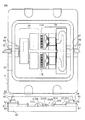
集積回路と、
付記1から9のいずれか1つ記載の伝送線路と、を備えることを特徴とする集積回路搭載装置。
(付記12)
前記伝送線路は、前記集積回路の出力側に設けられ、
前記集積回路の出力と、前記伝送線路の前記2本のテーパー線路の幅の広い側を接続するワイヤボンディングを備える付記11記載の集積回路搭載装置。
(付記13)
前記伝送線路は、前記集積回路の入力側と出力側の両方に設けられ、
前記集積回路の入力および出力と、前記伝送線路の前記2本のテーパー線路の幅の広い側を接続するワイヤボンディングを備える付記11記載の集積回路搭載装置。
(付記14)
前記集積回路は、前記伝送線路の前記2本のテーパー線路の幅の広い側に平行に配列された複数のトランジスタを備える付記11から13のいずれか記載の集積回路搭載装置。
(付記15)
付記11から14のいずれか記載の集積回路搭載装置を備える通信機モジュール。
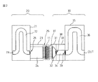
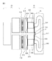
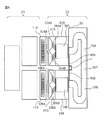
20 入力整合回路
30 出力整合回路
31A、31B、51 低誘電率基板
32AA、32AB、32BA、32BB テーパー線路
33A、33B 高誘電率基板
34A、34B 低インピーダンス線路
38AA、38AB、38BA、38BB ワイヤボンディング
42A、42B 抵抗
Claims (8)
- テーパー状の平面形状を有する並列に配置された2本のテーパー線路と、
前記2本のテーパー線路の幅の狭い側に対向して設けられた対向線路と、
前記2本のテーパー線路の幅の狭い側と、前記対向線路を接続するワイヤボンディングと、を備え、
並列に配置された前記2本のテーパー線路の幅の狭い側の2つの外側のエッジ間の幅は、前記2本のテーパー線路の幅の狭い側に対向する前記対向線路の対向側の外側のエッジ間の幅より大きいことを特徴とする伝送線路。 - 前記対向線路は、1本の対向線路であり、
並列に配置された前記2本のテーパー線路の幅の狭い側の2つの外側のエッジ間の幅は、前記1本の対向線路の前記対向側の幅より大きい請求項1記載の伝送線路。 - 前記対向線路は、2本の対向線路であり、
並列に配置された前記2本のテーパー線路の幅の狭い側の2つの外側のエッジ間の幅は、前記2本の対向線路の前記対向側の2つの外側のエッジ間の幅より大きい請求項1記載の伝送線路。 - 前記ワイヤボンディングは、第1の組と第2の組を備え、
前記第1の組の複数のワイヤは、前記対向線路の平面に投影した時に互いに平行な方向に伸び、
前記第2の組の複数のワイヤは、前記対向線路の平面に投影した時に、前記第1の組の複数のワイヤの伸びる方向と異なる方向に、互いに平行に伸びる請求項1から3のいずれか1項記載の伝送線路。 - 2本の第1の線路と、
第2の線路と、
前記2本の第1の線路と、前記第2の線路を接続するワイヤボンディングと、を備え、
前記ワイヤボンディングは、第1の組と第2の組を備え、
前記第1の組の複数のワイヤは、前記線路の平面に投影した時に互いに平行な方向に伸び、
前記第2の組の複数のワイヤは、前記線路の平面に投影した時に、前記第1の組の複数のワイヤの伸びる方向と異なる方向に、互いに平行に伸びることを特徴とする伝送線路。 - 集積回路と、
請求項1から5のいずれか1項記載の伝送線路と、を備えることを特徴とする集積回路搭載装置。 - 前記集積回路は、前記伝送線路の前記2本のテーパー線路の幅の広い側に平行に配列された複数のトランジスタを備える請求項6記載の集積回路搭載装置。
- 請求項6または7記載の集積回路搭載装置を備える通信機モジュール。
Priority Applications (6)
| Application Number | Priority Date | Filing Date | Title |
|---|---|---|---|
| JP2011015215A JP2012156362A (ja) | 2011-01-27 | 2011-01-27 | 伝送線路、集積回路搭載装置および通信機モジュール |
| EP11190255.7A EP2493008B1 (en) | 2011-01-27 | 2011-11-23 | Transmission line, impedance transformer, integrated circuit mounted device, and communication device module |
| CN201110384574.XA CN102623863B (zh) | 2011-01-27 | 2011-11-28 | 传输线、阻抗变换器、集成电路安装装置和通信装置模块 |
| TW100143705A TWI505542B (zh) | 2011-01-27 | 2011-11-29 | 傳輸線、阻抗轉換器、安裝有積體電路之裝置及通訊裝置模組 |
| KR1020110125693A KR101330853B1 (ko) | 2011-01-27 | 2011-11-29 | 전송 선로, 집적 회로 탑재 장치 및 통신기 모듈 |
| US13/306,641 US9007152B2 (en) | 2011-01-27 | 2011-11-29 | Transmission line, impedance transformer, integrated circuit mounted device, and communication device module |
Applications Claiming Priority (1)
| Application Number | Priority Date | Filing Date | Title |
|---|---|---|---|
| JP2011015215A JP2012156362A (ja) | 2011-01-27 | 2011-01-27 | 伝送線路、集積回路搭載装置および通信機モジュール |
Related Child Applications (1)
| Application Number | Title | Priority Date | Filing Date |
|---|---|---|---|
| JP2016145689A Division JP6354803B2 (ja) | 2016-07-25 | 2016-07-25 | 集積回路搭載装置および通信機モジュール |
Publications (1)
| Publication Number | Publication Date |
|---|---|
| JP2012156362A true JP2012156362A (ja) | 2012-08-16 |
Family
ID=45033855
Family Applications (1)
| Application Number | Title | Priority Date | Filing Date |
|---|---|---|---|
| JP2011015215A Pending JP2012156362A (ja) | 2011-01-27 | 2011-01-27 | 伝送線路、集積回路搭載装置および通信機モジュール |
Country Status (6)
| Country | Link |
|---|---|
| US (1) | US9007152B2 (ja) |
| EP (1) | EP2493008B1 (ja) |
| JP (1) | JP2012156362A (ja) |
| KR (1) | KR101330853B1 (ja) |
| CN (1) | CN102623863B (ja) |
| TW (1) | TWI505542B (ja) |
Families Citing this family (10)
| Publication number | Priority date | Publication date | Assignee | Title |
|---|---|---|---|---|
| US9570222B2 (en) * | 2013-05-28 | 2017-02-14 | Tdk Corporation | Vector inductor having multiple mutually coupled metalization layers providing high quality factor |
| CN103647131B (zh) * | 2013-12-11 | 2016-05-25 | 华为技术有限公司 | 一种改善微波电路耦合度波动的方法以及微波电路 |
| US9735752B2 (en) | 2014-12-03 | 2017-08-15 | Tdk Corporation | Apparatus and methods for tunable filters |
| KR102520393B1 (ko) * | 2015-11-11 | 2023-04-12 | 삼성전자주식회사 | 디지털 신호의 분기에 따른 반사 손실을 감소시키는 임피던스 매칭 소자 및 이를 포함하는 테스트 시스템 |
| KR102579321B1 (ko) * | 2016-06-28 | 2023-09-14 | 한국전자기술연구원 | 세라믹 기술을 이용한 내부 정합 및 내부 결합구조가 직접된 GaN 파워 트랜지스터 패키지 |
| US10978411B2 (en) * | 2016-11-18 | 2021-04-13 | Infineon Technologies Ag | RF power package having planar tuning lines |
| US11894322B2 (en) | 2018-05-29 | 2024-02-06 | Analog Devices, Inc. | Launch structures for radio frequency integrated device packages |
| US11424196B2 (en) | 2018-06-01 | 2022-08-23 | Analog Devices, Inc. | Matching circuit for integrated circuit die |
| US11417615B2 (en) * | 2018-11-27 | 2022-08-16 | Analog Devices, Inc. | Transition circuitry for integrated circuit die |
| US11744021B2 (en) | 2022-01-21 | 2023-08-29 | Analog Devices, Inc. | Electronic assembly |
Citations (2)
| Publication number | Priority date | Publication date | Assignee | Title |
|---|---|---|---|---|
| JPS57138422U (ja) * | 1981-02-25 | 1982-08-30 | ||
| JP2002335136A (ja) * | 2001-05-11 | 2002-11-22 | Matsushita Electric Ind Co Ltd | 高周波半導体装置 |
Family Cites Families (14)
| Publication number | Priority date | Publication date | Assignee | Title |
|---|---|---|---|---|
| JPS5737903A (en) | 1980-08-14 | 1982-03-02 | Nec Corp | Distribution constant type matching circuit |
| US4386324A (en) * | 1980-12-05 | 1983-05-31 | Hughes Aircraft Company | Planar chip-level power combiner |
| JPS6399604A (ja) * | 1986-10-15 | 1988-04-30 | Mitsubishi Electric Corp | 高周波半導体装置 |
| JPH0298503U (ja) * | 1989-01-24 | 1990-08-06 | ||
| US5132641A (en) * | 1991-05-01 | 1992-07-21 | Fujitsu Limited | Apparatus and method for dividing/combining microwave power from an odd number of transistor chips |
| JPH06104613A (ja) * | 1992-09-17 | 1994-04-15 | Mitsubishi Electric Corp | 高周波半導体装置 |
| JPH07283668A (ja) * | 1994-04-04 | 1995-10-27 | Mitsubishi Electric Corp | 高周波増幅器 |
| JPH07297609A (ja) * | 1994-04-28 | 1995-11-10 | Nec Yamagata Ltd | 半導体装置 |
| JP3566024B2 (ja) | 1997-03-31 | 2004-09-15 | 三菱電機株式会社 | アンテナ給電回路 |
| US5973567A (en) * | 1997-06-16 | 1999-10-26 | Hughes Electronics Corporation | Tunable impedance matching network for a mic power amplifier module |
| JPH11122009A (ja) | 1997-10-20 | 1999-04-30 | Fujitsu General Ltd | インピーダンス変換器 |
| JPH11238851A (ja) * | 1998-02-23 | 1999-08-31 | Hitachi Ltd | 集積回路装置およびそれを用いた通信機 |
| JP3303845B2 (ja) | 1999-05-26 | 2002-07-22 | 日本電気株式会社 | 内部整合型出力fet |
| JP5589428B2 (ja) * | 2010-02-19 | 2014-09-17 | 富士通株式会社 | 伝送線路、インピーダンス変換器、集積回路搭載装置および通信機モジュール |
-
2011
- 2011-01-27 JP JP2011015215A patent/JP2012156362A/ja active Pending
- 2011-11-23 EP EP11190255.7A patent/EP2493008B1/en active Active
- 2011-11-28 CN CN201110384574.XA patent/CN102623863B/zh active Active
- 2011-11-29 US US13/306,641 patent/US9007152B2/en active Active
- 2011-11-29 KR KR1020110125693A patent/KR101330853B1/ko active IP Right Grant
- 2011-11-29 TW TW100143705A patent/TWI505542B/zh active
Patent Citations (2)
| Publication number | Priority date | Publication date | Assignee | Title |
|---|---|---|---|---|
| JPS57138422U (ja) * | 1981-02-25 | 1982-08-30 | ||
| JP2002335136A (ja) * | 2001-05-11 | 2002-11-22 | Matsushita Electric Ind Co Ltd | 高周波半導体装置 |
Also Published As
| Publication number | Publication date |
|---|---|
| EP2493008A1 (en) | 2012-08-29 |
| US9007152B2 (en) | 2015-04-14 |
| KR101330853B1 (ko) | 2013-11-18 |
| CN102623863B (zh) | 2014-12-10 |
| US20120193771A1 (en) | 2012-08-02 |
| EP2493008B1 (en) | 2016-07-13 |
| TWI505542B (zh) | 2015-10-21 |
| TW201232912A (en) | 2012-08-01 |
| KR20120087072A (ko) | 2012-08-06 |
| CN102623863A (zh) | 2012-08-01 |
Similar Documents
| Publication | Publication Date | Title |
|---|---|---|
| KR101330853B1 (ko) | 전송 선로, 집적 회로 탑재 장치 및 통신기 모듈 | |
| US7952434B2 (en) | Semiconductor device | |
| JP5648295B2 (ja) | インピーダンス変換器、集積回路装置、増幅器および通信機モジュール | |
| US7768456B2 (en) | Antenna device and radio communication device | |
| JP5589428B2 (ja) | 伝送線路、インピーダンス変換器、集積回路搭載装置および通信機モジュール | |
| JP2011055241A (ja) | 高周波電力増幅器 | |
| US20220021404A1 (en) | Radio-frequency module and communication device | |
| JP6354803B2 (ja) | 集積回路搭載装置および通信機モジュール | |
| US20240154575A1 (en) | High frequency amplifier | |
| JP5812158B2 (ja) | 伝送線路、インピーダンス変換器、集積回路搭載装置および通信機モジュール | |
| JP2006528854A (ja) | 小型インピーダンス変換回路 | |
| JP5181424B2 (ja) | 高出力増幅器 | |
| JP2021069068A (ja) | 半導体装置 | |
| US11688916B2 (en) | Impedance converter and electronic device | |
| JP2011171576A (ja) | 集積回路装置、増幅器および通信機モジュール |
Legal Events
| Date | Code | Title | Description |
|---|---|---|---|
| A621 | Written request for application examination |
Free format text: JAPANESE INTERMEDIATE CODE: A621 Effective date: 20131007 |
|
| A977 | Report on retrieval |
Free format text: JAPANESE INTERMEDIATE CODE: A971007 Effective date: 20140725 |
|
| A131 | Notification of reasons for refusal |
Free format text: JAPANESE INTERMEDIATE CODE: A131 Effective date: 20140826 |
|
| A02 | Decision of refusal |
Free format text: JAPANESE INTERMEDIATE CODE: A02 Effective date: 20150428 |
|
| A521 | Written amendment |
Free format text: JAPANESE INTERMEDIATE CODE: A523 Effective date: 20150728 |
|
| A911 | Transfer to examiner for re-examination before appeal (zenchi) |
Free format text: JAPANESE INTERMEDIATE CODE: A911 Effective date: 20150806 |
|
| A912 | Re-examination (zenchi) completed and case transferred to appeal board |
Free format text: JAPANESE INTERMEDIATE CODE: A912 Effective date: 20151204 |
|
| A521 | Written amendment |
Free format text: JAPANESE INTERMEDIATE CODE: A523 Effective date: 20160725 |