JP2010282998A - 太陽電池、太陽電池の製造方法 - Google Patents
太陽電池、太陽電池の製造方法 Download PDFInfo
- Publication number
- JP2010282998A JP2010282998A JP2009132840A JP2009132840A JP2010282998A JP 2010282998 A JP2010282998 A JP 2010282998A JP 2009132840 A JP2009132840 A JP 2009132840A JP 2009132840 A JP2009132840 A JP 2009132840A JP 2010282998 A JP2010282998 A JP 2010282998A
- Authority
- JP
- Japan
- Prior art keywords
- layer
- electrode layer
- semiconductor layer
- solar cell
- electrode
- Prior art date
- Legal status (The legal status is an assumption and is not a legal conclusion. Google has not performed a legal analysis and makes no representation as to the accuracy of the status listed.)
- Withdrawn
Links
- 238000004519 manufacturing process Methods 0.000 title description 10
- 238000000034 method Methods 0.000 title description 9
- 239000004065 semiconductor Substances 0.000 claims abstract description 83
- 239000000758 substrate Substances 0.000 claims abstract description 34
- 239000010949 copper Substances 0.000 claims description 20
- RYGMFSIKBFXOCR-UHFFFAOYSA-N Copper Chemical compound [Cu] RYGMFSIKBFXOCR-UHFFFAOYSA-N 0.000 claims description 17
- 229910052802 copper Inorganic materials 0.000 claims description 17
- 239000000463 material Substances 0.000 claims description 14
- 238000010438 heat treatment Methods 0.000 claims description 8
- 150000001875 compounds Chemical class 0.000 claims description 7
- GYHNNYVSQQEPJS-UHFFFAOYSA-N Gallium Chemical compound [Ga] GYHNNYVSQQEPJS-UHFFFAOYSA-N 0.000 claims description 5
- 229910052733 gallium Inorganic materials 0.000 claims description 5
- 229910052738 indium Inorganic materials 0.000 claims description 5
- APFVFJFRJDLVQX-UHFFFAOYSA-N indium atom Chemical compound [In] APFVFJFRJDLVQX-UHFFFAOYSA-N 0.000 claims description 5
- 239000011669 selenium Substances 0.000 claims description 5
- BUGBHKTXTAQXES-UHFFFAOYSA-N Selenium Chemical compound [Se] BUGBHKTXTAQXES-UHFFFAOYSA-N 0.000 claims description 4
- 229910052711 selenium Inorganic materials 0.000 claims description 4
- 238000006243 chemical reaction Methods 0.000 abstract description 3
- 230000001747 exhibiting effect Effects 0.000 abstract 1
- 239000010408 film Substances 0.000 description 11
- XLOMVQKBTHCTTD-UHFFFAOYSA-N Zinc monoxide Chemical compound [Zn]=O XLOMVQKBTHCTTD-UHFFFAOYSA-N 0.000 description 9
- 239000010409 thin film Substances 0.000 description 8
- 230000004048 modification Effects 0.000 description 5
- 238000012986 modification Methods 0.000 description 5
- 229910052751 metal Inorganic materials 0.000 description 4
- 239000002184 metal Substances 0.000 description 4
- 239000011787 zinc oxide Substances 0.000 description 4
- WUPHOULIZUERAE-UHFFFAOYSA-N 3-(oxolan-2-yl)propanoic acid Chemical compound OC(=O)CCC1CCCO1 WUPHOULIZUERAE-UHFFFAOYSA-N 0.000 description 3
- 230000015572 biosynthetic process Effects 0.000 description 3
- 229910052980 cadmium sulfide Inorganic materials 0.000 description 3
- 230000000694 effects Effects 0.000 description 3
- 230000008569 process Effects 0.000 description 3
- 238000004544 sputter deposition Methods 0.000 description 3
- 229910001220 stainless steel Inorganic materials 0.000 description 3
- 239000010935 stainless steel Substances 0.000 description 3
- XKRFYHLGVUSROY-UHFFFAOYSA-N Argon Chemical compound [Ar] XKRFYHLGVUSROY-UHFFFAOYSA-N 0.000 description 2
- IJGRMHOSHXDMSA-UHFFFAOYSA-N Atomic nitrogen Chemical compound N#N IJGRMHOSHXDMSA-UHFFFAOYSA-N 0.000 description 2
- ZOKXTWBITQBERF-UHFFFAOYSA-N Molybdenum Chemical compound [Mo] ZOKXTWBITQBERF-UHFFFAOYSA-N 0.000 description 2
- 239000005357 flat glass Substances 0.000 description 2
- 239000007789 gas Substances 0.000 description 2
- 239000011521 glass Substances 0.000 description 2
- 239000010931 gold Substances 0.000 description 2
- 239000011261 inert gas Substances 0.000 description 2
- SHXXPRJOPFJRHA-UHFFFAOYSA-K iron(iii) fluoride Chemical compound F[Fe](F)F SHXXPRJOPFJRHA-UHFFFAOYSA-K 0.000 description 2
- BDAGIHXWWSANSR-UHFFFAOYSA-N methanoic acid Natural products OC=O BDAGIHXWWSANSR-UHFFFAOYSA-N 0.000 description 2
- 229910052750 molybdenum Inorganic materials 0.000 description 2
- 239000011733 molybdenum Substances 0.000 description 2
- 239000002243 precursor Substances 0.000 description 2
- OSWFIVFLDKOXQC-UHFFFAOYSA-N 4-(3-methoxyphenyl)aniline Chemical compound COC1=CC=CC(C=2C=CC(N)=CC=2)=C1 OSWFIVFLDKOXQC-UHFFFAOYSA-N 0.000 description 1
- YCKRFDGAMUMZLT-UHFFFAOYSA-N Fluorine atom Chemical compound [F] YCKRFDGAMUMZLT-UHFFFAOYSA-N 0.000 description 1
- UFHFLCQGNIYNRP-UHFFFAOYSA-N Hydrogen Chemical compound [H][H] UFHFLCQGNIYNRP-UHFFFAOYSA-N 0.000 description 1
- 239000004642 Polyimide Substances 0.000 description 1
- 229910004298 SiO 2 Inorganic materials 0.000 description 1
- VYPSYNLAJGMNEJ-UHFFFAOYSA-N Silicium dioxide Chemical compound O=[Si]=O VYPSYNLAJGMNEJ-UHFFFAOYSA-N 0.000 description 1
- XUIMIQQOPSSXEZ-UHFFFAOYSA-N Silicon Chemical compound [Si] XUIMIQQOPSSXEZ-UHFFFAOYSA-N 0.000 description 1
- BQCADISMDOOEFD-UHFFFAOYSA-N Silver Chemical compound [Ag] BQCADISMDOOEFD-UHFFFAOYSA-N 0.000 description 1
- 229910052786 argon Inorganic materials 0.000 description 1
- 230000008901 benefit Effects 0.000 description 1
- 230000008859 change Effects 0.000 description 1
- HPDFFVBPXCTEDN-UHFFFAOYSA-N copper manganese Chemical compound [Mn].[Cu] HPDFFVBPXCTEDN-UHFFFAOYSA-N 0.000 description 1
- 238000009792 diffusion process Methods 0.000 description 1
- 230000002708 enhancing effect Effects 0.000 description 1
- 239000011737 fluorine Substances 0.000 description 1
- 229910052731 fluorine Inorganic materials 0.000 description 1
- 235000019253 formic acid Nutrition 0.000 description 1
- PCHJSUWPFVWCPO-UHFFFAOYSA-N gold Chemical compound [Au] PCHJSUWPFVWCPO-UHFFFAOYSA-N 0.000 description 1
- 229910052737 gold Inorganic materials 0.000 description 1
- 239000001257 hydrogen Substances 0.000 description 1
- 229910052739 hydrogen Inorganic materials 0.000 description 1
- 238000009413 insulation Methods 0.000 description 1
- 239000010445 mica Substances 0.000 description 1
- 229910052618 mica group Inorganic materials 0.000 description 1
- 229910052757 nitrogen Inorganic materials 0.000 description 1
- 229920001721 polyimide Polymers 0.000 description 1
- 230000009467 reduction Effects 0.000 description 1
- SPVXKVOXSXTJOY-UHFFFAOYSA-N selane Chemical compound [SeH2] SPVXKVOXSXTJOY-UHFFFAOYSA-N 0.000 description 1
- 229910000058 selane Inorganic materials 0.000 description 1
- 229940065287 selenium compound Drugs 0.000 description 1
- 229910052710 silicon Inorganic materials 0.000 description 1
- 239000010703 silicon Substances 0.000 description 1
- 229910052814 silicon oxide Inorganic materials 0.000 description 1
- 229910052709 silver Inorganic materials 0.000 description 1
- 239000004332 silver Substances 0.000 description 1
- GKCNVZWZCYIBPR-UHFFFAOYSA-N sulfanylideneindium Chemical compound [In]=S GKCNVZWZCYIBPR-UHFFFAOYSA-N 0.000 description 1
Images


Classifications
-
- H—ELECTRICITY
- H01—ELECTRIC ELEMENTS
- H01L—SEMICONDUCTOR DEVICES NOT COVERED BY CLASS H10
- H01L31/00—Semiconductor devices sensitive to infrared radiation, light, electromagnetic radiation of shorter wavelength or corpuscular radiation and specially adapted either for the conversion of the energy of such radiation into electrical energy or for the control of electrical energy by such radiation; Processes or apparatus specially adapted for the manufacture or treatment thereof or of parts thereof; Details thereof
- H01L31/04—Semiconductor devices sensitive to infrared radiation, light, electromagnetic radiation of shorter wavelength or corpuscular radiation and specially adapted either for the conversion of the energy of such radiation into electrical energy or for the control of electrical energy by such radiation; Processes or apparatus specially adapted for the manufacture or treatment thereof or of parts thereof; Details thereof adapted as photovoltaic [PV] conversion devices
- H01L31/06—Semiconductor devices sensitive to infrared radiation, light, electromagnetic radiation of shorter wavelength or corpuscular radiation and specially adapted either for the conversion of the energy of such radiation into electrical energy or for the control of electrical energy by such radiation; Processes or apparatus specially adapted for the manufacture or treatment thereof or of parts thereof; Details thereof adapted as photovoltaic [PV] conversion devices characterised by at least one potential-jump barrier or surface barrier
- H01L31/072—Semiconductor devices sensitive to infrared radiation, light, electromagnetic radiation of shorter wavelength or corpuscular radiation and specially adapted either for the conversion of the energy of such radiation into electrical energy or for the control of electrical energy by such radiation; Processes or apparatus specially adapted for the manufacture or treatment thereof or of parts thereof; Details thereof adapted as photovoltaic [PV] conversion devices characterised by at least one potential-jump barrier or surface barrier the potential barriers being only of the PN heterojunction type
- H01L31/0749—Semiconductor devices sensitive to infrared radiation, light, electromagnetic radiation of shorter wavelength or corpuscular radiation and specially adapted either for the conversion of the energy of such radiation into electrical energy or for the control of electrical energy by such radiation; Processes or apparatus specially adapted for the manufacture or treatment thereof or of parts thereof; Details thereof adapted as photovoltaic [PV] conversion devices characterised by at least one potential-jump barrier or surface barrier the potential barriers being only of the PN heterojunction type including a AIBIIICVI compound, e.g. CdS/CulnSe2 [CIS] heterojunction solar cells
-
- H—ELECTRICITY
- H01—ELECTRIC ELEMENTS
- H01L—SEMICONDUCTOR DEVICES NOT COVERED BY CLASS H10
- H01L31/00—Semiconductor devices sensitive to infrared radiation, light, electromagnetic radiation of shorter wavelength or corpuscular radiation and specially adapted either for the conversion of the energy of such radiation into electrical energy or for the control of electrical energy by such radiation; Processes or apparatus specially adapted for the manufacture or treatment thereof or of parts thereof; Details thereof
- H01L31/02—Details
- H01L31/0224—Electrodes
- H01L31/022408—Electrodes for devices characterised by at least one potential jump barrier or surface barrier
- H01L31/022425—Electrodes for devices characterised by at least one potential jump barrier or surface barrier for solar cells
-
- H—ELECTRICITY
- H01—ELECTRIC ELEMENTS
- H01L—SEMICONDUCTOR DEVICES NOT COVERED BY CLASS H10
- H01L31/00—Semiconductor devices sensitive to infrared radiation, light, electromagnetic radiation of shorter wavelength or corpuscular radiation and specially adapted either for the conversion of the energy of such radiation into electrical energy or for the control of electrical energy by such radiation; Processes or apparatus specially adapted for the manufacture or treatment thereof or of parts thereof; Details thereof
- H01L31/0248—Semiconductor devices sensitive to infrared radiation, light, electromagnetic radiation of shorter wavelength or corpuscular radiation and specially adapted either for the conversion of the energy of such radiation into electrical energy or for the control of electrical energy by such radiation; Processes or apparatus specially adapted for the manufacture or treatment thereof or of parts thereof; Details thereof characterised by their semiconductor bodies
- H01L31/036—Semiconductor devices sensitive to infrared radiation, light, electromagnetic radiation of shorter wavelength or corpuscular radiation and specially adapted either for the conversion of the energy of such radiation into electrical energy or for the control of electrical energy by such radiation; Processes or apparatus specially adapted for the manufacture or treatment thereof or of parts thereof; Details thereof characterised by their semiconductor bodies characterised by their crystalline structure or particular orientation of the crystalline planes
- H01L31/0392—Semiconductor devices sensitive to infrared radiation, light, electromagnetic radiation of shorter wavelength or corpuscular radiation and specially adapted either for the conversion of the energy of such radiation into electrical energy or for the control of electrical energy by such radiation; Processes or apparatus specially adapted for the manufacture or treatment thereof or of parts thereof; Details thereof characterised by their semiconductor bodies characterised by their crystalline structure or particular orientation of the crystalline planes including thin films deposited on metallic or insulating substrates ; characterised by specific substrate materials or substrate features or by the presence of intermediate layers, e.g. barrier layers, on the substrate
- H01L31/03923—Semiconductor devices sensitive to infrared radiation, light, electromagnetic radiation of shorter wavelength or corpuscular radiation and specially adapted either for the conversion of the energy of such radiation into electrical energy or for the control of electrical energy by such radiation; Processes or apparatus specially adapted for the manufacture or treatment thereof or of parts thereof; Details thereof characterised by their semiconductor bodies characterised by their crystalline structure or particular orientation of the crystalline planes including thin films deposited on metallic or insulating substrates ; characterised by specific substrate materials or substrate features or by the presence of intermediate layers, e.g. barrier layers, on the substrate including AIBIIICVI compound materials, e.g. CIS, CIGS
-
- H—ELECTRICITY
- H01—ELECTRIC ELEMENTS
- H01L—SEMICONDUCTOR DEVICES NOT COVERED BY CLASS H10
- H01L31/00—Semiconductor devices sensitive to infrared radiation, light, electromagnetic radiation of shorter wavelength or corpuscular radiation and specially adapted either for the conversion of the energy of such radiation into electrical energy or for the control of electrical energy by such radiation; Processes or apparatus specially adapted for the manufacture or treatment thereof or of parts thereof; Details thereof
- H01L31/0248—Semiconductor devices sensitive to infrared radiation, light, electromagnetic radiation of shorter wavelength or corpuscular radiation and specially adapted either for the conversion of the energy of such radiation into electrical energy or for the control of electrical energy by such radiation; Processes or apparatus specially adapted for the manufacture or treatment thereof or of parts thereof; Details thereof characterised by their semiconductor bodies
- H01L31/036—Semiconductor devices sensitive to infrared radiation, light, electromagnetic radiation of shorter wavelength or corpuscular radiation and specially adapted either for the conversion of the energy of such radiation into electrical energy or for the control of electrical energy by such radiation; Processes or apparatus specially adapted for the manufacture or treatment thereof or of parts thereof; Details thereof characterised by their semiconductor bodies characterised by their crystalline structure or particular orientation of the crystalline planes
- H01L31/0392—Semiconductor devices sensitive to infrared radiation, light, electromagnetic radiation of shorter wavelength or corpuscular radiation and specially adapted either for the conversion of the energy of such radiation into electrical energy or for the control of electrical energy by such radiation; Processes or apparatus specially adapted for the manufacture or treatment thereof or of parts thereof; Details thereof characterised by their semiconductor bodies characterised by their crystalline structure or particular orientation of the crystalline planes including thin films deposited on metallic or insulating substrates ; characterised by specific substrate materials or substrate features or by the presence of intermediate layers, e.g. barrier layers, on the substrate
- H01L31/03925—Semiconductor devices sensitive to infrared radiation, light, electromagnetic radiation of shorter wavelength or corpuscular radiation and specially adapted either for the conversion of the energy of such radiation into electrical energy or for the control of electrical energy by such radiation; Processes or apparatus specially adapted for the manufacture or treatment thereof or of parts thereof; Details thereof characterised by their semiconductor bodies characterised by their crystalline structure or particular orientation of the crystalline planes including thin films deposited on metallic or insulating substrates ; characterised by specific substrate materials or substrate features or by the presence of intermediate layers, e.g. barrier layers, on the substrate including AIIBVI compound materials, e.g. CdTe, CdS
-
- H—ELECTRICITY
- H01—ELECTRIC ELEMENTS
- H01L—SEMICONDUCTOR DEVICES NOT COVERED BY CLASS H10
- H01L31/00—Semiconductor devices sensitive to infrared radiation, light, electromagnetic radiation of shorter wavelength or corpuscular radiation and specially adapted either for the conversion of the energy of such radiation into electrical energy or for the control of electrical energy by such radiation; Processes or apparatus specially adapted for the manufacture or treatment thereof or of parts thereof; Details thereof
- H01L31/04—Semiconductor devices sensitive to infrared radiation, light, electromagnetic radiation of shorter wavelength or corpuscular radiation and specially adapted either for the conversion of the energy of such radiation into electrical energy or for the control of electrical energy by such radiation; Processes or apparatus specially adapted for the manufacture or treatment thereof or of parts thereof; Details thereof adapted as photovoltaic [PV] conversion devices
- H01L31/042—PV modules or arrays of single PV cells
- H01L31/0445—PV modules or arrays of single PV cells including thin film solar cells, e.g. single thin film a-Si, CIS or CdTe solar cells
- H01L31/046—PV modules composed of a plurality of thin film solar cells deposited on the same substrate
-
- Y—GENERAL TAGGING OF NEW TECHNOLOGICAL DEVELOPMENTS; GENERAL TAGGING OF CROSS-SECTIONAL TECHNOLOGIES SPANNING OVER SEVERAL SECTIONS OF THE IPC; TECHNICAL SUBJECTS COVERED BY FORMER USPC CROSS-REFERENCE ART COLLECTIONS [XRACs] AND DIGESTS
- Y02—TECHNOLOGIES OR APPLICATIONS FOR MITIGATION OR ADAPTATION AGAINST CLIMATE CHANGE
- Y02E—REDUCTION OF GREENHOUSE GAS [GHG] EMISSIONS, RELATED TO ENERGY GENERATION, TRANSMISSION OR DISTRIBUTION
- Y02E10/00—Energy generation through renewable energy sources
- Y02E10/50—Photovoltaic [PV] energy
- Y02E10/541—CuInSe2 material PV cells
-
- Y—GENERAL TAGGING OF NEW TECHNOLOGICAL DEVELOPMENTS; GENERAL TAGGING OF CROSS-SECTIONAL TECHNOLOGIES SPANNING OVER SEVERAL SECTIONS OF THE IPC; TECHNICAL SUBJECTS COVERED BY FORMER USPC CROSS-REFERENCE ART COLLECTIONS [XRACs] AND DIGESTS
- Y02—TECHNOLOGIES OR APPLICATIONS FOR MITIGATION OR ADAPTATION AGAINST CLIMATE CHANGE
- Y02P—CLIMATE CHANGE MITIGATION TECHNOLOGIES IN THE PRODUCTION OR PROCESSING OF GOODS
- Y02P70/00—Climate change mitigation technologies in the production process for final industrial or consumer products
- Y02P70/50—Manufacturing or production processes characterised by the final manufactured product
Landscapes
- Engineering & Computer Science (AREA)
- Microelectronics & Electronic Packaging (AREA)
- Physics & Mathematics (AREA)
- Condensed Matter Physics & Semiconductors (AREA)
- Electromagnetism (AREA)
- General Physics & Mathematics (AREA)
- Computer Hardware Design (AREA)
- Power Engineering (AREA)
- Life Sciences & Earth Sciences (AREA)
- Sustainable Development (AREA)
- Sustainable Energy (AREA)
- Chemical & Material Sciences (AREA)
- Crystallography & Structural Chemistry (AREA)
- Photovoltaic Devices (AREA)
Abstract
【課題】変換効率の高い太陽電池を提供する。
【解決手段】基板と、前記基板上に形成された第1電極層と、前記第1電極層上に形成された半導体層と、前記半導体層上に形成された第2電極層と、を有し、前記半導体層の一部には、前記第1電極層から前記第2電極層に至る溝部が設けられ、前記溝部には、導電性を有するコンタクト層が形成された。
【選択図】図1
【解決手段】基板と、前記基板上に形成された第1電極層と、前記第1電極層上に形成された半導体層と、前記半導体層上に形成された第2電極層と、を有し、前記半導体層の一部には、前記第1電極層から前記第2電極層に至る溝部が設けられ、前記溝部には、導電性を有するコンタクト層が形成された。
【選択図】図1
Description
本発明は、太陽電池、太陽電池の製造方法に関する。
太陽電池は、光エネルギーを電気エネルギーに変換するものであり、使用される半導体によって様々な種類の構成が提案されている。近年では、製造工程が簡単で、高い変換効率が期待できるCIGS型の太陽電池が注目されている。CIGS型の太陽電池は、例えば、基板上に形成された第1電極膜と、第1電極膜上に形成された化合物半導体(銅−インジウム−ガリウム−セレン化合物)層を含む薄膜と、当該薄膜上に形成された第2電極膜と、で構成されている。そして、薄膜の一部が除去された溝内に第2電極膜が形成されており、第1電極膜と第2電極膜とが電気的に接続されている。(例えば、特許文献1参照)。
ところで、上記薄膜(化合物半導体層)の溝は、レーザー光照射や金属針等を用いて、薄膜の一部を除去することによって形成される。この際、上記溝内に薄膜の残渣が付着してしまうと、薄膜の残渣自体の抵抗が高いため、溝内に第2電極膜を形成して、第1電極膜と第2電極膜とを接続した際、第1電極膜と接続第2電極膜の間の電気的抵抗が高くなってしまうという、課題があった。
本発明は、上記課題の少なくとも一部を解決するためになされたものであり、以下の形態又は適用例として実現することが可能である。
[適用例1]本適用例にかかる太陽電池は、基板と、前記基板上に形成された第1電極層と、前記第1電極層上に形成された半導体層と、前記半導体層上に形成された第2電極層と、を有し、前記半導体層の一部には、前記第1電極層から前記第2電極層に至る溝部が設けられ、前記溝部には、導電性を有するコンタクト層が形成されたことを特徴とする。
この構成によれば、第1電極層と第2電極層は、半導体層の溝部に形成されたコンタクト層によって電気的に接続される。従って、容易に第1電極層と第2電極層との電気的接続性を確保することができる。
[適用例2]上記適用例にかかる太陽電池の前記コンタクト層は、前記第1電極層及び前記第2電極層よりも、電気抵抗率が低い材料で形成されたことを特徴とする。
この構成によれば、コンタクト層は、第1電極層及び第2電極層よりも、電気抵抗率が低くなるので、第1電極層と第2電極層との間における電気的抵抗を下げることができる。
[適用例3]上記適用例にかかる太陽電池の前記コンタクト層は、銅を主成分とする材料で形成されたことを特徴とする。
この構成によれば、コンタクト層は、比抵抗が小さい材料で形成されるので、第1電極層と第2電極層との間を低抵抗化させることができる。
[適用例4]上記適用例にかかる太陽電池の前記半導体層は、銅、インジウム、ガリウム、セレンを含む化合物半導体層を有し、前記コンタクト層は加熱処理により形成されることを特徴とする。
この構成によれば、半導体層は、銅、インジウム、ガリウム、セレンを含む化合物半導体(CIGS)層を有し、コンタクト層は、銅を主成分とする材料である。ここで、例えば、レーザー光照射や金属針等を用いて、化合物半導体層の一部を除去して溝部を形成すると、溝部内に化合物半導体層の残渣が付着してしまうことが考えられる。そこで、溝部内に銅を主成分とする材料を用い、加熱処理によってコンタクト層を形成することにより、加熱処理中に、残渣物を銅のコンタクト層に拡散させることができる。これにより、第1電極層と第2電極層との間における電気的抵抗を下げることができる。特に、第1電極層とコンタクト層との界面抵抗を下げることができる。
[適用例5]上記適用例にかかる太陽電池の前記コンタクト層は、前記半導体層の前記第2電極層方向の面と同一の高さとなるように、前記溝部に形成されたことを特徴とする。
この構成によれば、コンタクト層と半導体層との面が一の均一な面となる。すなわち、半導体層とコンタクト層の面には、段差等がない状態となる。従って、コンタクト層と第2電極層は、一平坦面で接続されるので、接続性を向上させることができる。
[適用例6]本適用例にかかる太陽電池の製造方法は、基板上に第1電極層を形成する第1電極層形成工程と、前記第1電極層上に半導体層を形成する半導体層形成工程と、前記半導体層の一部を厚み方向に除去し、前記第1電極層に至る溝部を形成する溝部形成工程と、前記溝部に導電性を有するコンタクト層を形成するコンタクト層形成工程と、前記半導体層および前記コンタクト層上に第2電極層を形成する第2電極層形成工程と、を含むことを特徴とする。
この構成によれば、第1電極層と第2電極層は、半導体層の溝部内に形成されたコンタクト層によって電気的に接続される。従って、容易に第1電極層と第2電極層との電気的接続性を確保することができる。
以下、本発明を具体化した実施形態について図面に従って説明する。なお、各図面における各部材は、各図面上で認識可能な程度の大きさとするため、各部材ごとに縮小を異ならせて図示している。
(太陽電池の構成)
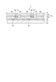
まず、太陽電池の構成について説明する。なお、本実施形態では、CIGS型の太陽電池の構成について説明する。図1は、本実施形態にかかる太陽電池の構成を示す断面図である。
まず、太陽電池の構成について説明する。なお、本実施形態では、CIGS型の太陽電池の構成について説明する。図1は、本実施形態にかかる太陽電池の構成を示す断面図である。
図1に示すように、太陽電池1は、基板10と、基板10上に形成された下地層11と、下地層11上に形成された第1電極層12と、第1電極層12上に形成された半導体層13と、半導体層13上に形成された第2電極層14と、第1電極層12と第2電極層14とを電気的に接続するコンタクト層17からなるセル40の集合体で構成されている。
隣接するセル40間は、第3分割溝33によって分割されている。また、第1電極層12は、第1分割溝31によってセル40単位で分割され、隣接するセル40間を跨ぐように形成されている。そして、半導体層13の一部に設けられた溝部としての第2分割溝32内にコンタクト層17が形成されており、第1電極層12と第2電極層14とが、コンタクト層17を介して接続される。そして、各セル40の第2電極層14が、隣接する他のセル40の第1電極層12と接続されることによって、各セル40が直列接続されている。このように、直列接続されたセル40の数を適宜設定することにより、太陽電池1における所望の電圧を任意に設計変更することが可能となる。
基板10は、少なくとも第1電極層12側の表面が絶縁性を有した基板である。具体的には、例えば、ガラス(青板ガラス等)基板、ステンレス基板、ポリイミド基板、雲母基板等を用いることができる。
下地層11は、基板10上に形成された絶縁性を有する層であり、例えば、SiO2(酸化珪素)を主成分とする絶縁層やフッ化鉄層を設けることができる。当該下地層11は、絶縁性を有するとともに、基板10と基板10上に形成された第1電極層12との密着性を確保する機能、および、基板が青板ガラスの場合は、ガラス基板10から第1電極層12へのNa拡散を防止する機能を併せ持つ。なお、基板10自体に上記特性を有している場合には、下地層11を省略することもできる。
第1電極層12は、下地層11上に形成された導電性を有する層であり、例えば、モリブデン(Mo)を用いることができる。
半導体層13は、第1半導体層13aと第2半導体層13bとで構成されている。第1半導体層13aは、第1電極層12上に形成され、銅(Cu)・インジウム(In)・ガリウム(Ga)・セレン(Se)を含むp型半導体層(CIGS半導体層)である。
第2半導体層13bは、第1半導体層13a上に形成され、硫化カドミウム(CdS)、酸化亜鉛(ZnO)、硫化インジウム(InS)等のn型半導体層である。
第2電極層14は、第2半導体層13b上に形成された透明性を有する電極層であり、例えば、AZO(Alドープ酸化亜鉛)等の透明電極体(TCO:Transparent Conducting Oxides)等である。
コンタクト層17は、導電性を有する層であり、第1電極層12及び第2電極層14よりも電気低効率が低い材料で形成されている。具体的には、銅(Cu)や銅を主成分とする材料が用いられる。なお、その他、金(Au)、銀(Ag)、銅−マンガン化合物等を用いることもできる。このように、電気抵抗率が低い材料を用いることにより、第1電極層12と第2電極層14との抵抗を下げることができる。また、本実施形態では、半導体層13に第2分割溝32が形成されており、当該第2分割溝32内にコンタクト層17が形成されている。さらに、コンタクト層17は、半導体層13の面と同一の高さとなるように形成される事がより望ましい。換言すれば、半導体層13の上面とコンタクト層17の上面が一の平坦面を形成し、当該平坦面上に第2電極層14が形成されることが望ましい。
上記のように構成されたCIGS型の太陽電池1に、太陽光等の光が入射されると、半導体層13内で電子(−)と正孔(+)の対が発生し、電子(−)と正孔(+)は、p型半導体(第1半導体層13a)とn型半導体(第2半導体層13b)との接合面で、電子(−)がn型半導体に集まり、正孔(+)がp型半導体に集まる。その結果、n型半導体とp型半導体との間に起電力が発生する。この状態で、第1電極層12と第2電極層14に外部導電線を接続することにより、電流を外部に取り出すことができる。
(太陽電池の製造方法)
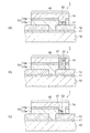
次に、太陽電池の製造方法について説明する。なお、本実施形態では、CIGS型の太陽電池の製造方法について説明する。図2及び図3は、本実施形態にかかる太陽電池の製造方法を示す工程図である。
次に、太陽電池の製造方法について説明する。なお、本実施形態では、CIGS型の太陽電池の製造方法について説明する。図2及び図3は、本実施形態にかかる太陽電池の製造方法を示す工程図である。
図2(a)の下地層形成工程では、ステンレスの基板10の一方面に下地層11を形成する。フッ化鉄からなる下地層11は、熱処理によって、ステンレスの基板10とフッ素含有ガスを反応させることにより形成することができる。本下地層11は、絶縁性を確保するとともに、第1電極層12と基板10間の密着力を高める効果を併せ持つ。なお、基板10自体に上記下地層効果を有している場合には、下地層形成工程を省略することができる。
図2(b)の第1電極層形成工程では、下地層11上に第1電極層12を形成する。具体的には、スパッタ法によって第1電極層12となるモリブデン(Mo)層を形成する。
図2(c)の第1分割工程では、第1電極層12の一部をレーザー光照射等によって除去し、第1電極層12を厚み方向に分割する。レーザー光照射等によって第1電極層12が除去された部分には、第1分割溝31が形成される。
図2(d)の第1半導体層形成工程では、まず、第1電極層12上および第1分割溝31内に、銅(Cu)、インジウム(In)およびガリウム(Ga)をスパッタ法等で付着させ、プリカーサーを形成する。そして、当該プリカーサーをセレン化水素雰囲気で加熱(セレン化)して、第1半導体層13aとなるp型の半導体層(CIGS)を形成する。
図2(e)の第2半導体層形成工程では、第1半導体層13a上にCdS、ZnOやInS等により第2半導体層13bとなるn型の半導体層を形成する。第2半導体層13bは、スパッタ法等によって形成することができる。
図3(f)の溝部形成工程(第2分割工程)では、レーザー光照射や金属針等により、半導体層13の一部を除去し、半導体層13を厚み方向に分割する。レーザー光照射等によって半導体層13が除去された部分には、溝部としての第2分割溝32が形成される。
図3(g)のコンタクト層形成工程では、第2分割溝32内にコンタクト層17を形成する。コンタクト層17の形成には、第1電極層12及び第2電極層14よりも電気抵抗率が低い材料を用いる。具体的には、銅を主成分とする材料を用いる。そして、印刷法やインクジェット法等によって、第2分割溝32内に銅を主成分とする材料を塗布し、窒素、もしくは、アルゴン等の不活性ガス雰囲気下、もしくは水素、蟻酸等の還元能をもつ成分を前記不活性ガスと混合した還元性ガス雰囲気下での熱処理等によって焼成する。これにより、コンタクト層17を形成することができる。また、コンタクト層17は、半導体層13の第2電極層14方向の底面と同一の高さ面となるように形成することが望ましい。半導体層13の第2電極層14の底面を同一の高さとした場合、半導体層13とコンタクト層17の面には、段差等の無い平坦面となる。
図3(h)の第2電極層形成工程では、半導体層13及びコンタクト層17上に第2電極層14を形成する。例えば、第2電極層となるAZO(ALドープ酸化亜鉛)等の透明電極(TCO)をスパッタ法等で形成する。
図3(i)の第3分割工程では、レーザー光照射や金属針等により、第2電極層14、半導体層13の一部を除去し、第2電極層14および半導体層13を厚み方向に分割する。レーザー光照射等によって第2電極層14および半導体層13が除去された部分には、第3分割溝33が形成され、一のセル40が形成される。
上記の工程を経ることより、複数のセル40が直列接続されたCIGS型の太陽電池1が形成される。
従って、上記の実施形態によれば、以下に示す効果がある。
(1)溝部としての第2分割溝32にコンタクト層17を形成し、当該コンタクト層17を介して第1電極層12と第2電極層14とを接続した。コンタクト層は、電気的効率の低い銅を主成分とする材料を用いた。これにより、第1電極層12と第2電極層14との間の抵抗を低減することができる。
(2)コンタクト層17は、半導体層13と同一面となるように形成した。これにより、コンタクト層17と第2電極層14との接続面に段差等がないので、接続性を向上させることができる。
(3)溝部形成(第2分割形成)工程の後に、コンタクト層17となる銅を第2分割溝32に塗布し、熱処理によってコンタクト層17を形成した。これにより、溝部形成(第2分割形成)工程において、第1半導体層13a(CIGS)の残渣が第2分割溝32に付着していたとしても、熱処理によって、残渣分が銅に拡散するため、第1電極層12とコンタクト層17の接続界面における界面抵抗を低減させることができる。
なお、上記の実施形態に限定されるものではなく、以下のような変形例が挙げられる。
(変形例1)上記実施形態では、半導体層13の面と均一になるように、かつ、第2分割溝32の内部全体にコンタクト層17を形成したが、これに限定されない。例えば、図4(a)に示すように、半導体層13の面よりも、コンタクト層17の面が低くなるように形成してもよいし、同図(b)に示すように、半導体層13の面よりも、コンタクト層17の面が高くなるように形成してもよい。さらには、同図(c)に示すように、第2分割溝32の内部の一部にコンタクト層17を設けてもよい。このようにしても、第1電極層12と第2電極層14との間の抵抗を低くすることができる。
(変形例2)上記実施形態では、第2電極層14側から光を受光する片面受光のCIGS型太陽電池1の構成等について説明したが、第2電極層14側からに加え、基板10側からも受光可能な両面受光のCIGS型太陽電池1であってもよい。なお、この場合、基板10は、透明性を有する基板を用いる。例えば、ガラス基板、PET、有機系透明基板等である。また、第1電極層12は、透明性を有する電極層とし、例えば、AZO(ALドープ酸化亜鉛)等の透明電極(TCO:Transparent Conducting Oxides)層とする。透明性を有する基板10を用い、かつ、第1電極層12に透明電極を用いることにより、基板10側からの入射した光は、第1電極層12を透過して半導体層13に到達し、光電変換に寄与する事が可能となる。上記両面受光のCIGS型太陽電池1でも、コンタクト層17を介して第1電極層12と第2電極層14とを電気的に接続することで、電極間の直列抵抗を低減することができる。
(変形例3)上記実施形態では、コンタクト層17をCIGS型の太陽電池に適用して説明したが、これに限定されない。例えば、薄膜シリコン型の太陽電池における電極接続構造に適用してもよい。このようにしても、電極間の直列抵抗を低減させることができる。
1…太陽電池、10…基板、11…下地層、12…第1電極層、13…半導体層、13a…第1半導体層、13b…第2半導体層、14…第2電極層、17…コンタクト層、31…第1分割溝、32…溝部としての第2分割溝、33…第3分割溝、40…セル。
Claims (6)
- 基板と、
前記基板上に形成された第1電極層と、
前記第1電極層上に形成された半導体層と、
前記半導体層上に形成された第2電極層と、を有し、
前記半導体層の一部には、前記第1電極層から前記第2電極層に至る溝部が設けられ、前記溝部には、導電性を有するコンタクト層が形成されたことを特徴とする太陽電池。 - 請求項1に記載の太陽電池において、
前記コンタクト層は、前記第1電極層及び前記第2電極層よりも、電気抵抗率が低い材料で形成されたことを特徴とする太陽電池。 - 請求項2に記載の太陽電池において、
前記コンタクト層は、銅を主成分とする材料で形成されたことを特徴とする太陽電池。 - 請求項3に記載の太陽電池において、
前記半導体層は、銅、インジウム、ガリウム、セレンを含む化合物半導体層を有し、前記コンタクト層は加熱処理により形成されることを特徴とする太陽電池。 - 請求項1〜4のいずれか一項に記載の太陽電池において、
前記コンタクト層は、前記半導体層の前記第2電極層方向の面と同一の高さとなるように、前記溝部に形成されたことを特徴とする太陽電池。 - 基板上に第1電極層を形成する第1電極層形成工程と、
前記第1電極層上に半導体層を形成する半導体層形成工程と、
前記半導体層の一部を厚み方向に除去し、前記第1電極層に至る溝部を形成する溝部形成工程と、
前記溝部に導電性を有するコンタクト層を形成するコンタクト層形成工程と、
前記半導体層および前記コンタクト層上に第2電極層を形成する第2電極層形成工程と、を含むことを特徴とする太陽電池の製造方法。
Priority Applications (3)
| Application Number | Priority Date | Filing Date | Title |
|---|---|---|---|
| JP2009132840A JP2010282998A (ja) | 2009-06-02 | 2009-06-02 | 太陽電池、太陽電池の製造方法 |
| US12/789,089 US20100300526A1 (en) | 2009-06-02 | 2010-05-27 | Solar cell and method for manufacturing solar cell |
| CN2010101964896A CN101908566A (zh) | 2009-06-02 | 2010-06-02 | 太阳电池及其制造方法 |
Applications Claiming Priority (1)
| Application Number | Priority Date | Filing Date | Title |
|---|---|---|---|
| JP2009132840A JP2010282998A (ja) | 2009-06-02 | 2009-06-02 | 太陽電池、太陽電池の製造方法 |
Publications (1)
| Publication Number | Publication Date |
|---|---|
| JP2010282998A true JP2010282998A (ja) | 2010-12-16 |
Family
ID=43218842
Family Applications (1)
| Application Number | Title | Priority Date | Filing Date |
|---|---|---|---|
| JP2009132840A Withdrawn JP2010282998A (ja) | 2009-06-02 | 2009-06-02 | 太陽電池、太陽電池の製造方法 |
Country Status (3)
| Country | Link |
|---|---|
| US (1) | US20100300526A1 (ja) |
| JP (1) | JP2010282998A (ja) |
| CN (1) | CN101908566A (ja) |
Families Citing this family (7)
| Publication number | Priority date | Publication date | Assignee | Title |
|---|---|---|---|---|
| TW201246560A (en) * | 2011-03-16 | 2012-11-16 | Stion Corp | A method for forming a bifacial thin film photovoltaic cell and a thin film solar device |
| US20130133732A1 (en) * | 2011-11-30 | 2013-05-30 | Taiwan Semiconductor Manufacturing Co., Ltd. | Method for forming interconnect in solar cell |
| FR2985607B1 (fr) * | 2012-01-11 | 2018-01-26 | Commissariat A L'energie Atomique Et Aux Energies Alternatives | Procede pour realiser un module photovoltaique avec deux etapes de gravure p1 et p3 et module photovoltaique correspondant. |
| FR2989224B1 (fr) * | 2012-04-06 | 2014-12-26 | Commissariat Energie Atomique | Procede pour realiser un module photovoltaique avec une etape de gravure p3 et une eventuelle etape p2. |
| FR2989223B1 (fr) | 2012-04-06 | 2014-12-26 | Commissariat Energie Atomique | Procede pour realiser un module photovoltaique avec une etape de gravure p3 et une eventuelle etape p1. |
| US9190322B2 (en) * | 2014-01-24 | 2015-11-17 | Infineon Technologies Ag | Method for producing a copper layer on a semiconductor body using a printing process |
| JP6955915B2 (ja) * | 2016-08-03 | 2021-10-27 | パナソニック株式会社 | 太陽電池モジュールおよびその製造方法 |
Citations (6)
| Publication number | Priority date | Publication date | Assignee | Title |
|---|---|---|---|---|
| JPH0494174A (ja) * | 1990-08-10 | 1992-03-26 | Fuji Electric Co Ltd | 化合物薄膜太陽電池およびその製造方法 |
| JPH09500236A (ja) * | 1993-07-20 | 1997-01-07 | シーメンス アクチエンゲゼルシヤフト | 薄膜太陽電池用の統合集積化レーザ構造化方法 |
| JP2002373995A (ja) * | 2001-06-15 | 2002-12-26 | Honda Motor Co Ltd | 太陽電池の製造方法 |
| JP2006528420A (ja) * | 2003-07-22 | 2006-12-14 | アクゾ ノーベル ナムローゼ フェンノートシャップ | 仮基板を用いた太陽電池箔の製造方法 |
| JP2007201304A (ja) * | 2006-01-30 | 2007-08-09 | Honda Motor Co Ltd | 太陽電池およびその製造方法 |
| JP2007317885A (ja) * | 2006-05-25 | 2007-12-06 | Honda Motor Co Ltd | 太陽電池およびその製造方法 |
Family Cites Families (9)
| Publication number | Priority date | Publication date | Assignee | Title |
|---|---|---|---|---|
| US8455753B2 (en) * | 2005-01-14 | 2013-06-04 | Semiconductor Energy Laboratory Co., Ltd. | Solar cell and semiconductor device, and manufacturing method thereof |
| US20070186971A1 (en) * | 2005-01-20 | 2007-08-16 | Nanosolar, Inc. | High-efficiency solar cell with insulated vias |
| JP4340246B2 (ja) * | 2005-03-07 | 2009-10-07 | シャープ株式会社 | 薄膜太陽電池およびその製造方法 |
| WO2006107154A1 (en) * | 2005-03-16 | 2006-10-12 | Korea Advanced Institute Of Science And Technology | Integrated thin-film solar cells and method of manufacturing thereof and processing method of transparent electrode for integrated thin-film solar cells and structure thereof, and transparent substrate having processed transparent electrode |
| EP1724844A2 (en) * | 2005-05-20 | 2006-11-22 | Semiconductor Energy Laboratory Co., Ltd. | Photoelectric conversion device, manufacturing method thereof and semiconductor device |
| KR20070101917A (ko) * | 2006-04-12 | 2007-10-18 | 엘지전자 주식회사 | 박막형 태양전지와 그의 제조방법 |
| JP4439492B2 (ja) * | 2006-05-25 | 2010-03-24 | 本田技研工業株式会社 | カルコパイライト型太陽電池およびその製造方法 |
| EP2234172A4 (en) * | 2008-01-15 | 2017-01-04 | Affinity Co., Ltd. | Solar cell module and method for manufacturing the same |
| US20090229666A1 (en) * | 2008-03-14 | 2009-09-17 | Jason Stephan Corneille | Smoothing a metallic substrate for a solar cell |
-
2009
- 2009-06-02 JP JP2009132840A patent/JP2010282998A/ja not_active Withdrawn
-
2010
- 2010-05-27 US US12/789,089 patent/US20100300526A1/en not_active Abandoned
- 2010-06-02 CN CN2010101964896A patent/CN101908566A/zh active Pending
Patent Citations (6)
| Publication number | Priority date | Publication date | Assignee | Title |
|---|---|---|---|---|
| JPH0494174A (ja) * | 1990-08-10 | 1992-03-26 | Fuji Electric Co Ltd | 化合物薄膜太陽電池およびその製造方法 |
| JPH09500236A (ja) * | 1993-07-20 | 1997-01-07 | シーメンス アクチエンゲゼルシヤフト | 薄膜太陽電池用の統合集積化レーザ構造化方法 |
| JP2002373995A (ja) * | 2001-06-15 | 2002-12-26 | Honda Motor Co Ltd | 太陽電池の製造方法 |
| JP2006528420A (ja) * | 2003-07-22 | 2006-12-14 | アクゾ ノーベル ナムローゼ フェンノートシャップ | 仮基板を用いた太陽電池箔の製造方法 |
| JP2007201304A (ja) * | 2006-01-30 | 2007-08-09 | Honda Motor Co Ltd | 太陽電池およびその製造方法 |
| JP2007317885A (ja) * | 2006-05-25 | 2007-12-06 | Honda Motor Co Ltd | 太陽電池およびその製造方法 |
Also Published As
| Publication number | Publication date |
|---|---|
| CN101908566A (zh) | 2010-12-08 |
| US20100300526A1 (en) | 2010-12-02 |
Similar Documents
| Publication | Publication Date | Title |
|---|---|---|
| JP2010282997A (ja) | 太陽電池、太陽電池の製造方法 | |
| JP2010282998A (ja) | 太陽電池、太陽電池の製造方法 | |
| JP2013510426A (ja) | 太陽電池及びその製造方法 | |
| JPWO2010001473A1 (ja) | 光起電力装置およびその製造方法 | |
| JP2011023442A (ja) | 太陽電池、太陽電池の製造方法 | |
| KR101283072B1 (ko) | 태양광 발전장치 및 이의 제조방법 | |
| KR101091375B1 (ko) | 태양 전지 및 이의 제조 방법 | |
| KR101091379B1 (ko) | 태양전지 및 이의 제조방법 | |
| KR101380540B1 (ko) | 태양전지의 금속전극 형성방법 | |
| CN104272470A (zh) | 太阳能电池及其制造方法 | |
| JP2011023622A (ja) | 太陽電池、太陽電池の製造方法 | |
| KR101241467B1 (ko) | 태양전지 및 이의 제조방법 | |
| KR101067807B1 (ko) | 태양전지 셀 및 그의 전극 형성 방법 | |
| KR101091359B1 (ko) | 태양전지 및 이의 제조방법 | |
| KR101154571B1 (ko) | 태양전지 모듈 및 이의 제조방법 | |
| KR20130136739A (ko) | 태양전지 및 이의 제조방법 | |
| JP2011023443A (ja) | 太陽電池、太陽電池の製造方法 | |
| KR20120086447A (ko) | 태양전지 및 이의 제조방법 | |
| CN104067398A (zh) | 太阳能电池及其制造方法 | |
| KR101220015B1 (ko) | 태양전지 및 이의 제조방법 | |
| JP2011066045A (ja) | 太陽電池の製造方法 | |
| KR20130059976A (ko) | 태양전지 및 이의 제조방법 | |
| KR101765922B1 (ko) | 태양전지 및 이의 제조방법 | |
| KR101020941B1 (ko) | 태양전지 및 이의 제조방법 | |
| KR101273123B1 (ko) | 태양전지 및 이의 제조방법 |
Legal Events
| Date | Code | Title | Description |
|---|---|---|---|
| A621 | Written request for application examination |
Free format text: JAPANESE INTERMEDIATE CODE: A621 Effective date: 20120406 |
|
| A977 | Report on retrieval |
Free format text: JAPANESE INTERMEDIATE CODE: A971007 Effective date: 20130327 |
|
| A131 | Notification of reasons for refusal |
Free format text: JAPANESE INTERMEDIATE CODE: A131 Effective date: 20130507 |
|
| A761 | Written withdrawal of application |
Free format text: JAPANESE INTERMEDIATE CODE: A761 Effective date: 20130626 |