JP2010199528A - ボンディングワイヤ - Google Patents
ボンディングワイヤInfo
- Publication number
- JP2010199528A JP2010199528A JP2009094065A JP2009094065A JP2010199528A JP 2010199528 A JP2010199528 A JP 2010199528A JP 2009094065 A JP2009094065 A JP 2009094065A JP 2009094065 A JP2009094065 A JP 2009094065A JP 2010199528 A JP2010199528 A JP 2010199528A
- Authority
- JP
- Japan
- Prior art keywords
- wire
- coating layer
- bonding
- copper
- bonding wire
- Prior art date
- Legal status (The legal status is an assumption and is not a legal conclusion. Google has not performed a legal analysis and makes no representation as to the accuracy of the status listed.)
- Pending
Links
Images

Classifications
-
- H—ELECTRICITY
- H10—SEMICONDUCTOR DEVICES; ELECTRIC SOLID-STATE DEVICES NOT OTHERWISE PROVIDED FOR
- H10W—GENERIC PACKAGES, INTERCONNECTIONS, CONNECTORS OR OTHER CONSTRUCTIONAL DETAILS OF DEVICES COVERED BY CLASS H10
- H10W72/00—Interconnections or connectors in packages
- H10W72/071—Connecting or disconnecting
- H10W72/075—Connecting or disconnecting of bond wires
-
- H—ELECTRICITY
- H10—SEMICONDUCTOR DEVICES; ELECTRIC SOLID-STATE DEVICES NOT OTHERWISE PROVIDED FOR
- H10W—GENERIC PACKAGES, INTERCONNECTIONS, CONNECTORS OR OTHER CONSTRUCTIONAL DETAILS OF DEVICES COVERED BY CLASS H10
- H10W72/00—Interconnections or connectors in packages
- H10W72/01—Manufacture or treatment
- H10W72/015—Manufacture or treatment of bond wires
- H10W72/01551—Changing the shapes of bond wires
-
- H—ELECTRICITY
- H10—SEMICONDUCTOR DEVICES; ELECTRIC SOLID-STATE DEVICES NOT OTHERWISE PROVIDED FOR
- H10W—GENERIC PACKAGES, INTERCONNECTIONS, CONNECTORS OR OTHER CONSTRUCTIONAL DETAILS OF DEVICES COVERED BY CLASS H10
- H10W72/00—Interconnections or connectors in packages
- H10W72/01—Manufacture or treatment
- H10W72/015—Manufacture or treatment of bond wires
- H10W72/01565—Thermally treating
-
- H—ELECTRICITY
- H10—SEMICONDUCTOR DEVICES; ELECTRIC SOLID-STATE DEVICES NOT OTHERWISE PROVIDED FOR
- H10W—GENERIC PACKAGES, INTERCONNECTIONS, CONNECTORS OR OTHER CONSTRUCTIONAL DETAILS OF DEVICES COVERED BY CLASS H10
- H10W72/00—Interconnections or connectors in packages
- H10W72/071—Connecting or disconnecting
- H10W72/0711—Apparatus therefor
- H10W72/07141—Means for applying energy, e.g. ovens or lasers
-
- H—ELECTRICITY
- H10—SEMICONDUCTOR DEVICES; ELECTRIC SOLID-STATE DEVICES NOT OTHERWISE PROVIDED FOR
- H10W—GENERIC PACKAGES, INTERCONNECTIONS, CONNECTORS OR OTHER CONSTRUCTIONAL DETAILS OF DEVICES COVERED BY CLASS H10
- H10W72/00—Interconnections or connectors in packages
- H10W72/071—Connecting or disconnecting
- H10W72/075—Connecting or disconnecting of bond wires
- H10W72/07511—Treating the bonding area before connecting, e.g. by applying flux or cleaning
-
- H—ELECTRICITY
- H10—SEMICONDUCTOR DEVICES; ELECTRIC SOLID-STATE DEVICES NOT OTHERWISE PROVIDED FOR
- H10W—GENERIC PACKAGES, INTERCONNECTIONS, CONNECTORS OR OTHER CONSTRUCTIONAL DETAILS OF DEVICES COVERED BY CLASS H10
- H10W72/00—Interconnections or connectors in packages
- H10W72/071—Connecting or disconnecting
- H10W72/075—Connecting or disconnecting of bond wires
- H10W72/07521—Aligning
-
- H—ELECTRICITY
- H10—SEMICONDUCTOR DEVICES; ELECTRIC SOLID-STATE DEVICES NOT OTHERWISE PROVIDED FOR
- H10W—GENERIC PACKAGES, INTERCONNECTIONS, CONNECTORS OR OTHER CONSTRUCTIONAL DETAILS OF DEVICES COVERED BY CLASS H10
- H10W72/00—Interconnections or connectors in packages
- H10W72/071—Connecting or disconnecting
- H10W72/075—Connecting or disconnecting of bond wires
- H10W72/07531—Techniques
- H10W72/07532—Compression bonding, e.g. thermocompression bonding
- H10W72/07533—Ultrasonic bonding, e.g. thermosonic bonding
-
- H—ELECTRICITY
- H10—SEMICONDUCTOR DEVICES; ELECTRIC SOLID-STATE DEVICES NOT OTHERWISE PROVIDED FOR
- H10W—GENERIC PACKAGES, INTERCONNECTIONS, CONNECTORS OR OTHER CONSTRUCTIONAL DETAILS OF DEVICES COVERED BY CLASS H10
- H10W72/00—Interconnections or connectors in packages
- H10W72/071—Connecting or disconnecting
- H10W72/075—Connecting or disconnecting of bond wires
- H10W72/07551—Connecting or disconnecting of bond wires characterised by changes in properties of the bond wires during the connecting
- H10W72/07553—Connecting or disconnecting of bond wires characterised by changes in properties of the bond wires during the connecting changes in shapes
-
- H—ELECTRICITY
- H10—SEMICONDUCTOR DEVICES; ELECTRIC SOLID-STATE DEVICES NOT OTHERWISE PROVIDED FOR
- H10W—GENERIC PACKAGES, INTERCONNECTIONS, CONNECTORS OR OTHER CONSTRUCTIONAL DETAILS OF DEVICES COVERED BY CLASS H10
- H10W72/00—Interconnections or connectors in packages
- H10W72/50—Bond wires
- H10W72/521—Structures or relative sizes of bond wires
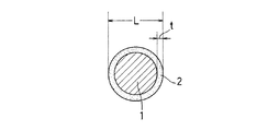
- H10W72/522—Multilayered bond wires, e.g. having a coating concentric around a core
-
- H—ELECTRICITY
- H10—SEMICONDUCTOR DEVICES; ELECTRIC SOLID-STATE DEVICES NOT OTHERWISE PROVIDED FOR
- H10W—GENERIC PACKAGES, INTERCONNECTIONS, CONNECTORS OR OTHER CONSTRUCTIONAL DETAILS OF DEVICES COVERED BY CLASS H10
- H10W72/00—Interconnections or connectors in packages
- H10W72/50—Bond wires
- H10W72/531—Shapes of wire connectors
- H10W72/5363—Shapes of wire connectors the connected ends being wedge-shaped
-
- H—ELECTRICITY
- H10—SEMICONDUCTOR DEVICES; ELECTRIC SOLID-STATE DEVICES NOT OTHERWISE PROVIDED FOR
- H10W—GENERIC PACKAGES, INTERCONNECTIONS, CONNECTORS OR OTHER CONSTRUCTIONAL DETAILS OF DEVICES COVERED BY CLASS H10
- H10W72/00—Interconnections or connectors in packages
- H10W72/50—Bond wires
- H10W72/531—Shapes of wire connectors
- H10W72/5366—Shapes of wire connectors the bond wires having kinks
-
- H—ELECTRICITY
- H10—SEMICONDUCTOR DEVICES; ELECTRIC SOLID-STATE DEVICES NOT OTHERWISE PROVIDED FOR
- H10W—GENERIC PACKAGES, INTERCONNECTIONS, CONNECTORS OR OTHER CONSTRUCTIONAL DETAILS OF DEVICES COVERED BY CLASS H10
- H10W72/00—Interconnections or connectors in packages
- H10W72/50—Bond wires
- H10W72/551—Materials of bond wires
- H10W72/552—Materials of bond wires comprising metals or metalloids, e.g. silver
- H10W72/5522—Materials of bond wires comprising metals or metalloids, e.g. silver comprising gold [Au]
-
- H—ELECTRICITY
- H10—SEMICONDUCTOR DEVICES; ELECTRIC SOLID-STATE DEVICES NOT OTHERWISE PROVIDED FOR
- H10W—GENERIC PACKAGES, INTERCONNECTIONS, CONNECTORS OR OTHER CONSTRUCTIONAL DETAILS OF DEVICES COVERED BY CLASS H10
- H10W72/00—Interconnections or connectors in packages
- H10W72/50—Bond wires
- H10W72/551—Materials of bond wires
- H10W72/552—Materials of bond wires comprising metals or metalloids, e.g. silver
- H10W72/5525—Materials of bond wires comprising metals or metalloids, e.g. silver comprising copper [Cu]
-
- H—ELECTRICITY
- H10—SEMICONDUCTOR DEVICES; ELECTRIC SOLID-STATE DEVICES NOT OTHERWISE PROVIDED FOR
- H10W—GENERIC PACKAGES, INTERCONNECTIONS, CONNECTORS OR OTHER CONSTRUCTIONAL DETAILS OF DEVICES COVERED BY CLASS H10
- H10W72/00—Interconnections or connectors in packages
- H10W72/50—Bond wires
- H10W72/551—Materials of bond wires
- H10W72/555—Materials of bond wires of outermost layers of multilayered bond wires, e.g. material of a coating
Landscapes
- Wire Bonding (AREA)
Priority Applications (3)
| Application Number | Priority Date | Filing Date | Title |
|---|---|---|---|
| JP2009094065A JP2010199528A (ja) | 2009-01-27 | 2009-04-08 | ボンディングワイヤ |
| PCT/JP2009/065735 WO2010087053A1 (ja) | 2009-01-27 | 2009-09-09 | ボンディングワイヤ |
| TW099102279A TW201037777A (en) | 2009-01-27 | 2010-01-27 | Bonding wire |
Applications Claiming Priority (2)
| Application Number | Priority Date | Filing Date | Title |
|---|---|---|---|
| JP2009015265 | 2009-01-27 | ||
| JP2009094065A JP2010199528A (ja) | 2009-01-27 | 2009-04-08 | ボンディングワイヤ |
Publications (2)
| Publication Number | Publication Date |
|---|---|
| JP2010199528A true JP2010199528A (ja) | 2010-09-09 |
| JP2010199528A5 JP2010199528A5 (https=) | 2011-05-12 |
Family
ID=42395321
Family Applications (1)
| Application Number | Title | Priority Date | Filing Date |
|---|---|---|---|
| JP2009094065A Pending JP2010199528A (ja) | 2009-01-27 | 2009-04-08 | ボンディングワイヤ |
Country Status (3)
| Country | Link |
|---|---|
| JP (1) | JP2010199528A (https=) |
| TW (1) | TW201037777A (https=) |
| WO (1) | WO2010087053A1 (https=) |
Cited By (37)
| Publication number | Priority date | Publication date | Assignee | Title |
|---|---|---|---|---|
| JP2014513439A (ja) * | 2011-05-03 | 2014-05-29 | テッセラ,インコーポレイテッド | 封止表面に至るワイヤボンドを有するパッケージ・オン・パッケージアセンブリ |
| US9391008B2 (en) | 2012-07-31 | 2016-07-12 | Invensas Corporation | Reconstituted wafer-level package DRAM |
| US9412714B2 (en) | 2014-05-30 | 2016-08-09 | Invensas Corporation | Wire bond support structure and microelectronic package including wire bonds therefrom |
| US9502390B2 (en) | 2012-08-03 | 2016-11-22 | Invensas Corporation | BVA interposer |
| US9553076B2 (en) | 2010-07-19 | 2017-01-24 | Tessera, Inc. | Stackable molded microelectronic packages with area array unit connectors |
| US9570416B2 (en) | 2004-11-03 | 2017-02-14 | Tessera, Inc. | Stacked packaging improvements |
| US9570382B2 (en) | 2010-07-19 | 2017-02-14 | Tessera, Inc. | Stackable molded microelectronic packages |
| US9583411B2 (en) | 2014-01-17 | 2017-02-28 | Invensas Corporation | Fine pitch BVA using reconstituted wafer with area array accessible for testing |
| US9601454B2 (en) | 2013-02-01 | 2017-03-21 | Invensas Corporation | Method of forming a component having wire bonds and a stiffening layer |
| US9615456B2 (en) | 2012-12-20 | 2017-04-04 | Invensas Corporation | Microelectronic assembly for microelectronic packaging with bond elements to encapsulation surface |
| US9659848B1 (en) | 2015-11-18 | 2017-05-23 | Invensas Corporation | Stiffened wires for offset BVA |
| US9685365B2 (en) | 2013-08-08 | 2017-06-20 | Invensas Corporation | Method of forming a wire bond having a free end |
| US9691679B2 (en) | 2012-02-24 | 2017-06-27 | Invensas Corporation | Method for package-on-package assembly with wire bonds to encapsulation surface |
| US9728527B2 (en) | 2013-11-22 | 2017-08-08 | Invensas Corporation | Multiple bond via arrays of different wire heights on a same substrate |
| US9735084B2 (en) | 2014-12-11 | 2017-08-15 | Invensas Corporation | Bond via array for thermal conductivity |
| US9761558B2 (en) | 2011-10-17 | 2017-09-12 | Invensas Corporation | Package-on-package assembly with wire bond vias |
| US9761554B2 (en) | 2015-05-07 | 2017-09-12 | Invensas Corporation | Ball bonding metal wire bond wires to metal pads |
| US9812402B2 (en) | 2015-10-12 | 2017-11-07 | Invensas Corporation | Wire bond wires for interference shielding |
| US9842745B2 (en) | 2012-02-17 | 2017-12-12 | Invensas Corporation | Heat spreading substrate with embedded interconnects |
| US9852969B2 (en) | 2013-11-22 | 2017-12-26 | Invensas Corporation | Die stacks with one or more bond via arrays of wire bond wires and with one or more arrays of bump interconnects |
| US9888579B2 (en) | 2015-03-05 | 2018-02-06 | Invensas Corporation | Pressing of wire bond wire tips to provide bent-over tips |
| US9911718B2 (en) | 2015-11-17 | 2018-03-06 | Invensas Corporation | ‘RDL-First’ packaged microelectronic device for a package-on-package device |
| US9935075B2 (en) | 2016-07-29 | 2018-04-03 | Invensas Corporation | Wire bonding method and apparatus for electromagnetic interference shielding |
| US9953914B2 (en) | 2012-05-22 | 2018-04-24 | Invensas Corporation | Substrate-less stackable package with wire-bond interconnect |
| US9984901B2 (en) | 2005-12-23 | 2018-05-29 | Tessera, Inc. | Method for making a microelectronic assembly having conductive elements |
| US9984992B2 (en) | 2015-12-30 | 2018-05-29 | Invensas Corporation | Embedded wire bond wires for vertical integration with separate surface mount and wire bond mounting surfaces |
| US10008477B2 (en) | 2013-09-16 | 2018-06-26 | Invensas Corporation | Microelectronic element with bond elements to encapsulation surface |
| US10008469B2 (en) | 2015-04-30 | 2018-06-26 | Invensas Corporation | Wafer-level packaging using wire bond wires in place of a redistribution layer |
| US10026717B2 (en) | 2013-11-22 | 2018-07-17 | Invensas Corporation | Multiple bond via arrays of different wire heights on a same substrate |
| US10181457B2 (en) | 2015-10-26 | 2019-01-15 | Invensas Corporation | Microelectronic package for wafer-level chip scale packaging with fan-out |
| CN109411591A (zh) * | 2018-09-14 | 2019-03-01 | 汕头市骏码凯撒有限公司 | 一种led封装用银合金线及其制作方法 |
| US10299368B2 (en) | 2016-12-21 | 2019-05-21 | Invensas Corporation | Surface integrated waveguides and circuit structures therefor |
| US10332854B2 (en) | 2015-10-23 | 2019-06-25 | Invensas Corporation | Anchoring structure of fine pitch bva |
| US10381326B2 (en) | 2014-05-28 | 2019-08-13 | Invensas Corporation | Structure and method for integrated circuits packaging with increased density |
| US10460958B2 (en) | 2013-08-07 | 2019-10-29 | Invensas Corporation | Method of manufacturing embedded packaging with preformed vias |
| US10490528B2 (en) | 2015-10-12 | 2019-11-26 | Invensas Corporation | Embedded wire bond wires |
| JP2021093473A (ja) * | 2019-12-12 | 2021-06-17 | ローム株式会社 | 半導体装置および半導体装置の製造方法 |
Families Citing this family (5)
| Publication number | Priority date | Publication date | Assignee | Title |
|---|---|---|---|---|
| CN102130068B (zh) * | 2011-01-07 | 2012-09-05 | 四川威纳尔特种电子材料有限公司 | 一种表面有复合镀层的合金型键合丝 |
| JP4860004B1 (ja) * | 2011-02-28 | 2012-01-25 | タツタ電線株式会社 | ボンディングワイヤ及びその製造方法 |
| CN102324392B (zh) * | 2011-10-19 | 2013-03-27 | 广东佳博电子科技有限公司 | 一种防氧化的铜基键合丝的制备工艺 |
| CN103219247B (zh) * | 2013-03-01 | 2015-11-25 | 溧阳市虹翔机械制造有限公司 | 一种镀银键合铜丝的制造方法 |
| CN103219246B (zh) * | 2013-03-01 | 2015-11-25 | 溧阳市虹翔机械制造有限公司 | 一种镀钯镀银的双镀层键合铜丝的制造方法 |
Citations (2)
| Publication number | Priority date | Publication date | Assignee | Title |
|---|---|---|---|---|
| JPS6297360A (ja) * | 1985-10-24 | 1987-05-06 | Mitsubishi Metal Corp | 半導体装置のボンデイングワイヤ用表面被覆高純度銅極細線 |
| JP2004064033A (ja) * | 2001-10-23 | 2004-02-26 | Sumitomo Electric Wintec Inc | ボンディングワイヤー |
Family Cites Families (4)
| Publication number | Priority date | Publication date | Assignee | Title |
|---|---|---|---|---|
| JPS6278863A (ja) * | 1985-09-30 | 1987-04-11 | Tanaka Denshi Kogyo Kk | 半導体素子のボンデイング用銅線 |
| JPH0786325A (ja) * | 1993-09-14 | 1995-03-31 | Hitachi Cable Ltd | 電子機器用銅線 |
| MY137479A (en) * | 2000-09-18 | 2009-01-30 | Nippon Steel Corp | Bonding wire for semiconductor device and method for producing the same |
| JP2003133361A (ja) * | 2001-10-23 | 2003-05-09 | Sumiden Magnet Wire Kk | ボンディングワイヤー |
-
2009
- 2009-04-08 JP JP2009094065A patent/JP2010199528A/ja active Pending
- 2009-09-09 WO PCT/JP2009/065735 patent/WO2010087053A1/ja not_active Ceased
-
2010
- 2010-01-27 TW TW099102279A patent/TW201037777A/zh unknown
Patent Citations (2)
| Publication number | Priority date | Publication date | Assignee | Title |
|---|---|---|---|---|
| JPS6297360A (ja) * | 1985-10-24 | 1987-05-06 | Mitsubishi Metal Corp | 半導体装置のボンデイングワイヤ用表面被覆高純度銅極細線 |
| JP2004064033A (ja) * | 2001-10-23 | 2004-02-26 | Sumitomo Electric Wintec Inc | ボンディングワイヤー |
Cited By (66)
| Publication number | Priority date | Publication date | Assignee | Title |
|---|---|---|---|---|
| US9570416B2 (en) | 2004-11-03 | 2017-02-14 | Tessera, Inc. | Stacked packaging improvements |
| US9984901B2 (en) | 2005-12-23 | 2018-05-29 | Tessera, Inc. | Method for making a microelectronic assembly having conductive elements |
| US10128216B2 (en) | 2010-07-19 | 2018-11-13 | Tessera, Inc. | Stackable molded microelectronic packages |
| US9553076B2 (en) | 2010-07-19 | 2017-01-24 | Tessera, Inc. | Stackable molded microelectronic packages with area array unit connectors |
| US9570382B2 (en) | 2010-07-19 | 2017-02-14 | Tessera, Inc. | Stackable molded microelectronic packages |
| JP2014513439A (ja) * | 2011-05-03 | 2014-05-29 | テッセラ,インコーポレイテッド | 封止表面に至るワイヤボンドを有するパッケージ・オン・パッケージアセンブリ |
| JP2017041643A (ja) * | 2011-05-03 | 2017-02-23 | テッセラ,インコーポレイテッド | 封止表面に至るワイヤボンドを有するパッケージ・オン・パッケージアセンブリ |
| US11424211B2 (en) | 2011-05-03 | 2022-08-23 | Tessera Llc | Package-on-package assembly with wire bonds to encapsulation surface |
| US10062661B2 (en) | 2011-05-03 | 2018-08-28 | Tessera, Inc. | Package-on-package assembly with wire bonds to encapsulation surface |
| US10593643B2 (en) | 2011-05-03 | 2020-03-17 | Tessera, Inc. | Package-on-package assembly with wire bonds to encapsulation surface |
| US9691731B2 (en) | 2011-05-03 | 2017-06-27 | Tessera, Inc. | Package-on-package assembly with wire bonds to encapsulation surface |
| US11735563B2 (en) | 2011-10-17 | 2023-08-22 | Invensas Llc | Package-on-package assembly with wire bond vias |
| US11189595B2 (en) | 2011-10-17 | 2021-11-30 | Invensas Corporation | Package-on-package assembly with wire bond vias |
| US9761558B2 (en) | 2011-10-17 | 2017-09-12 | Invensas Corporation | Package-on-package assembly with wire bond vias |
| US10756049B2 (en) | 2011-10-17 | 2020-08-25 | Invensas Corporation | Package-on-package assembly with wire bond vias |
| US9842745B2 (en) | 2012-02-17 | 2017-12-12 | Invensas Corporation | Heat spreading substrate with embedded interconnects |
| US9691679B2 (en) | 2012-02-24 | 2017-06-27 | Invensas Corporation | Method for package-on-package assembly with wire bonds to encapsulation surface |
| US10170412B2 (en) | 2012-05-22 | 2019-01-01 | Invensas Corporation | Substrate-less stackable package with wire-bond interconnect |
| US9953914B2 (en) | 2012-05-22 | 2018-04-24 | Invensas Corporation | Substrate-less stackable package with wire-bond interconnect |
| US10510659B2 (en) | 2012-05-22 | 2019-12-17 | Invensas Corporation | Substrate-less stackable package with wire-bond interconnect |
| US9917073B2 (en) | 2012-07-31 | 2018-03-13 | Invensas Corporation | Reconstituted wafer-level package dram with conductive interconnects formed in encapsulant at periphery of the package |
| US9391008B2 (en) | 2012-07-31 | 2016-07-12 | Invensas Corporation | Reconstituted wafer-level package DRAM |
| US10297582B2 (en) | 2012-08-03 | 2019-05-21 | Invensas Corporation | BVA interposer |
| US9502390B2 (en) | 2012-08-03 | 2016-11-22 | Invensas Corporation | BVA interposer |
| US9615456B2 (en) | 2012-12-20 | 2017-04-04 | Invensas Corporation | Microelectronic assembly for microelectronic packaging with bond elements to encapsulation surface |
| US9601454B2 (en) | 2013-02-01 | 2017-03-21 | Invensas Corporation | Method of forming a component having wire bonds and a stiffening layer |
| US10460958B2 (en) | 2013-08-07 | 2019-10-29 | Invensas Corporation | Method of manufacturing embedded packaging with preformed vias |
| US9685365B2 (en) | 2013-08-08 | 2017-06-20 | Invensas Corporation | Method of forming a wire bond having a free end |
| US10008477B2 (en) | 2013-09-16 | 2018-06-26 | Invensas Corporation | Microelectronic element with bond elements to encapsulation surface |
| US9728527B2 (en) | 2013-11-22 | 2017-08-08 | Invensas Corporation | Multiple bond via arrays of different wire heights on a same substrate |
| US9852969B2 (en) | 2013-11-22 | 2017-12-26 | Invensas Corporation | Die stacks with one or more bond via arrays of wire bond wires and with one or more arrays of bump interconnects |
| US10290613B2 (en) | 2013-11-22 | 2019-05-14 | Invensas Corporation | Multiple bond via arrays of different wire heights on a same substrate |
| US10629567B2 (en) | 2013-11-22 | 2020-04-21 | Invensas Corporation | Multiple plated via arrays of different wire heights on same substrate |
| US10026717B2 (en) | 2013-11-22 | 2018-07-17 | Invensas Corporation | Multiple bond via arrays of different wire heights on a same substrate |
| USRE49987E1 (en) | 2013-11-22 | 2024-05-28 | Invensas Llc | Multiple plated via arrays of different wire heights on a same substrate |
| US11990382B2 (en) | 2014-01-17 | 2024-05-21 | Adeia Semiconductor Technologies Llc | Fine pitch BVA using reconstituted wafer with area array accessible for testing |
| US9837330B2 (en) | 2014-01-17 | 2017-12-05 | Invensas Corporation | Fine pitch BVA using reconstituted wafer with area array accessible for testing |
| US9583411B2 (en) | 2014-01-17 | 2017-02-28 | Invensas Corporation | Fine pitch BVA using reconstituted wafer with area array accessible for testing |
| US10529636B2 (en) | 2014-01-17 | 2020-01-07 | Invensas Corporation | Fine pitch BVA using reconstituted wafer with area array accessible for testing |
| US11404338B2 (en) | 2014-01-17 | 2022-08-02 | Invensas Corporation | Fine pitch bva using reconstituted wafer with area array accessible for testing |
| US10381326B2 (en) | 2014-05-28 | 2019-08-13 | Invensas Corporation | Structure and method for integrated circuits packaging with increased density |
| US9412714B2 (en) | 2014-05-30 | 2016-08-09 | Invensas Corporation | Wire bond support structure and microelectronic package including wire bonds therefrom |
| US9947641B2 (en) | 2014-05-30 | 2018-04-17 | Invensas Corporation | Wire bond support structure and microelectronic package including wire bonds therefrom |
| US9735084B2 (en) | 2014-12-11 | 2017-08-15 | Invensas Corporation | Bond via array for thermal conductivity |
| US9888579B2 (en) | 2015-03-05 | 2018-02-06 | Invensas Corporation | Pressing of wire bond wire tips to provide bent-over tips |
| US10806036B2 (en) | 2015-03-05 | 2020-10-13 | Invensas Corporation | Pressing of wire bond wire tips to provide bent-over tips |
| US10008469B2 (en) | 2015-04-30 | 2018-06-26 | Invensas Corporation | Wafer-level packaging using wire bond wires in place of a redistribution layer |
| US9761554B2 (en) | 2015-05-07 | 2017-09-12 | Invensas Corporation | Ball bonding metal wire bond wires to metal pads |
| US10115678B2 (en) | 2015-10-12 | 2018-10-30 | Invensas Corporation | Wire bond wires for interference shielding |
| US9812402B2 (en) | 2015-10-12 | 2017-11-07 | Invensas Corporation | Wire bond wires for interference shielding |
| US10490528B2 (en) | 2015-10-12 | 2019-11-26 | Invensas Corporation | Embedded wire bond wires |
| US10559537B2 (en) | 2015-10-12 | 2020-02-11 | Invensas Corporation | Wire bond wires for interference shielding |
| US11462483B2 (en) | 2015-10-12 | 2022-10-04 | Invensas Llc | Wire bond wires for interference shielding |
| US10332854B2 (en) | 2015-10-23 | 2019-06-25 | Invensas Corporation | Anchoring structure of fine pitch bva |
| US10181457B2 (en) | 2015-10-26 | 2019-01-15 | Invensas Corporation | Microelectronic package for wafer-level chip scale packaging with fan-out |
| US9911718B2 (en) | 2015-11-17 | 2018-03-06 | Invensas Corporation | ‘RDL-First’ packaged microelectronic device for a package-on-package device |
| US10043779B2 (en) | 2015-11-17 | 2018-08-07 | Invensas Corporation | Packaged microelectronic device for a package-on-package device |
| US9659848B1 (en) | 2015-11-18 | 2017-05-23 | Invensas Corporation | Stiffened wires for offset BVA |
| US10325877B2 (en) | 2015-12-30 | 2019-06-18 | Invensas Corporation | Embedded wire bond wires for vertical integration with separate surface mount and wire bond mounting surfaces |
| US9984992B2 (en) | 2015-12-30 | 2018-05-29 | Invensas Corporation | Embedded wire bond wires for vertical integration with separate surface mount and wire bond mounting surfaces |
| US10658302B2 (en) | 2016-07-29 | 2020-05-19 | Invensas Corporation | Wire bonding method and apparatus for electromagnetic interference shielding |
| US9935075B2 (en) | 2016-07-29 | 2018-04-03 | Invensas Corporation | Wire bonding method and apparatus for electromagnetic interference shielding |
| US10299368B2 (en) | 2016-12-21 | 2019-05-21 | Invensas Corporation | Surface integrated waveguides and circuit structures therefor |
| CN109411591A (zh) * | 2018-09-14 | 2019-03-01 | 汕头市骏码凯撒有限公司 | 一种led封装用银合金线及其制作方法 |
| JP2021093473A (ja) * | 2019-12-12 | 2021-06-17 | ローム株式会社 | 半導体装置および半導体装置の製造方法 |
| JP7412998B2 (ja) | 2019-12-12 | 2024-01-15 | ローム株式会社 | 半導体装置および半導体装置の製造方法 |
Also Published As
| Publication number | Publication date |
|---|---|
| TW201037777A (en) | 2010-10-16 |
| WO2010087053A1 (ja) | 2010-08-05 |
Similar Documents
| Publication | Publication Date | Title |
|---|---|---|
| JP2010199528A (ja) | ボンディングワイヤ | |
| JP5616739B2 (ja) | 複層銅ボンディングワイヤの接合構造 | |
| KR101707244B1 (ko) | 반도체용 본딩 와이어 | |
| KR101536554B1 (ko) | 본딩용 와이어 | |
| JP2010245390A (ja) | ボンディングワイヤ | |
| JP4637256B1 (ja) | 半導体用ボンディングワイヤー | |
| JP4672373B2 (ja) | 半導体装置用ボンディングワイヤ | |
| JPWO2011129256A1 (ja) | ボンディングワイヤ | |
| JP5497360B2 (ja) | 半導体用ボンディングワイヤー | |
| JP2011146754A (ja) | ボンディングワイヤの接合構造及びその形成方法 | |
| JP5343069B2 (ja) | ボンディングワイヤの接合構造 | |
| JP5064577B2 (ja) | ボールボンディング用ワイヤ | |
| WO2013018238A1 (ja) | ボールボンディングワイヤ | |
| JP5671512B2 (ja) | ボンディング用ワイヤ | |
| JP2004014884A (ja) | ボンディングワイヤー | |
| JP5393614B2 (ja) | 半導体装置用ボンディングワイヤ | |
| JP4860004B1 (ja) | ボンディングワイヤ及びその製造方法 | |
| JP5996853B2 (ja) | ボールボンディング用ワイヤ | |
| JP5591987B2 (ja) | 半導体装置用ボンディングワイヤ | |
| JP2011222882A (ja) | ボンディングワイヤ | |
| JP5001455B1 (ja) | ボンディングワイヤ及びその製造方法 | |
| JP2011249463A (ja) | ボンディングワイヤ | |
| JP2013042105A (ja) | ボンディングワイヤ | |
| JP2010245574A (ja) | 半導体装置用ボンディングワイヤ |
Legal Events
| Date | Code | Title | Description |
|---|---|---|---|
| A711 | Notification of change in applicant |
Free format text: JAPANESE INTERMEDIATE CODE: A712 Effective date: 20100701 |
|
| A521 | Request for written amendment filed |
Free format text: JAPANESE INTERMEDIATE CODE: A523 Effective date: 20110325 |
|
| A621 | Written request for application examination |
Free format text: JAPANESE INTERMEDIATE CODE: A621 Effective date: 20110325 |
|
| A871 | Explanation of circumstances concerning accelerated examination |
Free format text: JAPANESE INTERMEDIATE CODE: A871 Effective date: 20110325 |
|
| A975 | Report on accelerated examination |
Free format text: JAPANESE INTERMEDIATE CODE: A971005 Effective date: 20110407 |
|
| A131 | Notification of reasons for refusal |
Free format text: JAPANESE INTERMEDIATE CODE: A131 Effective date: 20110412 |
|
| A521 | Request for written amendment filed |
Free format text: JAPANESE INTERMEDIATE CODE: A523 Effective date: 20110510 |
|
| A02 | Decision of refusal |
Free format text: JAPANESE INTERMEDIATE CODE: A02 Effective date: 20110524 |