JP2010147500A - 半導体デバイス - Google Patents
半導体デバイス Download PDFInfo
- Publication number
- JP2010147500A JP2010147500A JP2010037667A JP2010037667A JP2010147500A JP 2010147500 A JP2010147500 A JP 2010147500A JP 2010037667 A JP2010037667 A JP 2010037667A JP 2010037667 A JP2010037667 A JP 2010037667A JP 2010147500 A JP2010147500 A JP 2010147500A
- Authority
- JP
- Japan
- Prior art keywords
- semiconductor device
- inner layer
- layer
- area
- integrated circuit
- Prior art date
- Legal status (The legal status is an assumption and is not a legal conclusion. Google has not performed a legal analysis and makes no representation as to the accuracy of the status listed.)
- Granted
Links
Images
Classifications
-
- H—ELECTRICITY
- H10—SEMICONDUCTOR DEVICES; ELECTRIC SOLID-STATE DEVICES NOT OTHERWISE PROVIDED FOR
- H10W—GENERIC PACKAGES, INTERCONNECTIONS, CONNECTORS OR OTHER CONSTRUCTIONAL DETAILS OF DEVICES COVERED BY CLASS H10
- H10W74/00—Encapsulations, e.g. protective coatings
- H10W74/10—Encapsulations, e.g. protective coatings characterised by their shape or disposition
- H10W74/111—Encapsulations, e.g. protective coatings characterised by their shape or disposition the semiconductor body being completely enclosed
- H10W74/121—Encapsulations, e.g. protective coatings characterised by their shape or disposition the semiconductor body being completely enclosed by multiple encapsulations, e.g. by a thin protective coating and a thick encapsulation
-
- H—ELECTRICITY
- H10—SEMICONDUCTOR DEVICES; ELECTRIC SOLID-STATE DEVICES NOT OTHERWISE PROVIDED FOR
- H10W—GENERIC PACKAGES, INTERCONNECTIONS, CONNECTORS OR OTHER CONSTRUCTIONAL DETAILS OF DEVICES COVERED BY CLASS H10
- H10W72/00—Interconnections or connectors in packages
- H10W72/071—Connecting or disconnecting
- H10W72/072—Connecting or disconnecting of bump connectors
- H10W72/07251—Connecting or disconnecting of bump connectors characterised by changes in properties of the bump connectors during connecting
-
- H—ELECTRICITY
- H10—SEMICONDUCTOR DEVICES; ELECTRIC SOLID-STATE DEVICES NOT OTHERWISE PROVIDED FOR
- H10W—GENERIC PACKAGES, INTERCONNECTIONS, CONNECTORS OR OTHER CONSTRUCTIONAL DETAILS OF DEVICES COVERED BY CLASS H10
- H10W72/00—Interconnections or connectors in packages
- H10W72/071—Connecting or disconnecting
- H10W72/075—Connecting or disconnecting of bond wires
-
- H—ELECTRICITY
- H10—SEMICONDUCTOR DEVICES; ELECTRIC SOLID-STATE DEVICES NOT OTHERWISE PROVIDED FOR
- H10W—GENERIC PACKAGES, INTERCONNECTIONS, CONNECTORS OR OTHER CONSTRUCTIONAL DETAILS OF DEVICES COVERED BY CLASS H10
- H10W72/00—Interconnections or connectors in packages
- H10W72/20—Bump connectors, e.g. solder bumps or copper pillars; Dummy bumps; Thermal bumps
-
- H—ELECTRICITY
- H10—SEMICONDUCTOR DEVICES; ELECTRIC SOLID-STATE DEVICES NOT OTHERWISE PROVIDED FOR
- H10W—GENERIC PACKAGES, INTERCONNECTIONS, CONNECTORS OR OTHER CONSTRUCTIONAL DETAILS OF DEVICES COVERED BY CLASS H10
- H10W72/00—Interconnections or connectors in packages
- H10W72/50—Bond wires
- H10W72/531—Shapes of wire connectors
- H10W72/536—Shapes of wire connectors the connected ends being ball-shaped
-
- H—ELECTRICITY
- H10—SEMICONDUCTOR DEVICES; ELECTRIC SOLID-STATE DEVICES NOT OTHERWISE PROVIDED FOR
- H10W—GENERIC PACKAGES, INTERCONNECTIONS, CONNECTORS OR OTHER CONSTRUCTIONAL DETAILS OF DEVICES COVERED BY CLASS H10
- H10W72/00—Interconnections or connectors in packages
- H10W72/50—Bond wires
- H10W72/531—Shapes of wire connectors
- H10W72/5363—Shapes of wire connectors the connected ends being wedge-shaped
-
- H—ELECTRICITY
- H10—SEMICONDUCTOR DEVICES; ELECTRIC SOLID-STATE DEVICES NOT OTHERWISE PROVIDED FOR
- H10W—GENERIC PACKAGES, INTERCONNECTIONS, CONNECTORS OR OTHER CONSTRUCTIONAL DETAILS OF DEVICES COVERED BY CLASS H10
- H10W72/00—Interconnections or connectors in packages
- H10W72/50—Bond wires
- H10W72/551—Materials of bond wires
-
- H—ELECTRICITY
- H10—SEMICONDUCTOR DEVICES; ELECTRIC SOLID-STATE DEVICES NOT OTHERWISE PROVIDED FOR
- H10W—GENERIC PACKAGES, INTERCONNECTIONS, CONNECTORS OR OTHER CONSTRUCTIONAL DETAILS OF DEVICES COVERED BY CLASS H10
- H10W72/00—Interconnections or connectors in packages
- H10W72/851—Dispositions of multiple connectors or interconnections
- H10W72/874—On different surfaces
- H10W72/884—Die-attach connectors and bond wires
-
- H—ELECTRICITY
- H10—SEMICONDUCTOR DEVICES; ELECTRIC SOLID-STATE DEVICES NOT OTHERWISE PROVIDED FOR
- H10W—GENERIC PACKAGES, INTERCONNECTIONS, CONNECTORS OR OTHER CONSTRUCTIONAL DETAILS OF DEVICES COVERED BY CLASS H10
- H10W72/00—Interconnections or connectors in packages
- H10W72/90—Bond pads, in general
- H10W72/951—Materials of bond pads
- H10W72/952—Materials of bond pads comprising metals or metalloids, e.g. PbSn, Ag or Cu
-
- H—ELECTRICITY
- H10—SEMICONDUCTOR DEVICES; ELECTRIC SOLID-STATE DEVICES NOT OTHERWISE PROVIDED FOR
- H10W—GENERIC PACKAGES, INTERCONNECTIONS, CONNECTORS OR OTHER CONSTRUCTIONAL DETAILS OF DEVICES COVERED BY CLASS H10
- H10W74/00—Encapsulations, e.g. protective coatings
-
- H—ELECTRICITY
- H10—SEMICONDUCTOR DEVICES; ELECTRIC SOLID-STATE DEVICES NOT OTHERWISE PROVIDED FOR
- H10W—GENERIC PACKAGES, INTERCONNECTIONS, CONNECTORS OR OTHER CONSTRUCTIONAL DETAILS OF DEVICES COVERED BY CLASS H10
- H10W90/00—Package configurations
- H10W90/701—Package configurations characterised by the relative positions of pads or connectors relative to package parts
- H10W90/731—Package configurations characterised by the relative positions of pads or connectors relative to package parts of die-attach connectors
- H10W90/736—Package configurations characterised by the relative positions of pads or connectors relative to package parts of die-attach connectors between a chip and a stacked lead frame, conducting package substrate or heat sink
-
- H—ELECTRICITY
- H10—SEMICONDUCTOR DEVICES; ELECTRIC SOLID-STATE DEVICES NOT OTHERWISE PROVIDED FOR
- H10W—GENERIC PACKAGES, INTERCONNECTIONS, CONNECTORS OR OTHER CONSTRUCTIONAL DETAILS OF DEVICES COVERED BY CLASS H10
- H10W90/00—Package configurations
- H10W90/701—Package configurations characterised by the relative positions of pads or connectors relative to package parts
- H10W90/751—Package configurations characterised by the relative positions of pads or connectors relative to package parts of bond wires
- H10W90/756—Package configurations characterised by the relative positions of pads or connectors relative to package parts of bond wires between a chip and a stacked lead frame, conducting package substrate or heat sink
Landscapes
- Structures Or Materials For Encapsulating Or Coating Semiconductor Devices Or Solid State Devices (AREA)
- Encapsulation Of And Coatings For Semiconductor Or Solid State Devices (AREA)
- Internal Circuitry In Semiconductor Integrated Circuit Devices (AREA)
Abstract
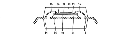
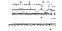
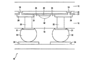
【解決手段】キャリア及び集積回路(10)を有する半導体デバイスにおいて、前記集積回路は、1つ以上の半導体素子と、前記半導体素子が接している1つ以上の接続領域と、前記接続領域を覆うパッシベーションレイヤ(20)とを有し、エンベロープにより周囲から絶縁され、前記エンベロープは相互境界面を持つ内部レイヤ(21)及び外部レイヤ(16)を有し、前記キャリアは、前記接続領域に接続手段により接続される導電部分を有し、前記相互境界面が、前記内部レイヤと前記外部レイヤとが分離した領域である層間剥離エリア(22)を完全に囲み、その結果、前記層間剥離エリアが前記接続領域から絶縁される。
【選択図】図3
Description
Claims (7)
- キャリア及び集積回路を有する半導体デバイスであり、
前記集積回路は、1つ以上の半導体素子と、前記半導体素子が接している1つ以上の接続領域と、前記接続領域を覆うパッシベーションレイヤとを有し、エンベロープにより周囲から絶縁され、前記エンベロープは相互境界面を持つ内部レイヤ及び外部レイヤを有し、
前記キャリアは、前記接続領域に接続手段により接続される導電部分を有し、
前記相互境界面が、前記内部レイヤと前記外部レイヤとが分離した領域である層間剥離エリアを完全に囲み、その結果、前記層間剥離エリアが前記接続領域から絶縁されることを特徴とする半導体デバイス。 - 前記層間剥離エリア及び前記相互境界面は、前記内部レイヤの表面上に置かれ、前記層間剥離エリアは前記内部レイヤの表面エリアの30%から70%の間の大きさであることを特徴とする請求項1に記載の半導体デバイス。
- 前記パッシベーションレイヤと前記内部レイヤは前記接続領域にあるボンディングパッドが露出したままであることを特徴とする請求項1に記載の半導体デバイス。
- 一定量の硬化される合成樹脂が前記層間剥離エリアに置かれることを特徴とする請求項1に記載の半導体デバイス。
- 前記エンベロープは前記キャリアに、又はキャリア上に取り付けられることを特徴とする請求項1に記載の半導体デバイス。
- 前記キャリアはリードフレームであることを特徴とする請求項1に記載の半導体デバイス。
- 前記一定量の硬化される合成樹脂はエポキシ樹脂であることを特徴とする請求項4に記載の半導体デバイス。
Applications Claiming Priority (2)
| Application Number | Priority Date | Filing Date | Title |
|---|---|---|---|
| EP01204504 | 2001-11-23 | ||
| EP01204504.3 | 2001-11-23 |
Related Parent Applications (1)
| Application Number | Title | Priority Date | Filing Date |
|---|---|---|---|
| JP2003546400A Division JP4583757B2 (ja) | 2001-11-23 | 2002-11-20 | 集積回路を包む方法 |
Publications (2)
| Publication Number | Publication Date |
|---|---|
| JP2010147500A true JP2010147500A (ja) | 2010-07-01 |
| JP5220783B2 JP5220783B2 (ja) | 2013-06-26 |
Family
ID=8181283
Family Applications (2)
| Application Number | Title | Priority Date | Filing Date |
|---|---|---|---|
| JP2003546400A Expired - Lifetime JP4583757B2 (ja) | 2001-11-23 | 2002-11-20 | 集積回路を包む方法 |
| JP2010037667A Expired - Lifetime JP5220783B2 (ja) | 2001-11-23 | 2010-02-23 | 半導体デバイス |
Family Applications Before (1)
| Application Number | Title | Priority Date | Filing Date |
|---|---|---|---|
| JP2003546400A Expired - Lifetime JP4583757B2 (ja) | 2001-11-23 | 2002-11-20 | 集積回路を包む方法 |
Country Status (6)
| Country | Link |
|---|---|
| US (1) | US7098545B2 (ja) |
| EP (1) | EP1451869B1 (ja) |
| JP (2) | JP4583757B2 (ja) |
| CN (1) | CN1288750C (ja) |
| AU (1) | AU2002351024A1 (ja) |
| WO (1) | WO2003044858A2 (ja) |
Families Citing this family (7)
| Publication number | Priority date | Publication date | Assignee | Title |
|---|---|---|---|---|
| DE102006017115B4 (de) * | 2006-04-10 | 2008-08-28 | Infineon Technologies Ag | Halbleiterbauteil mit einem Kunststoffgehäuse und Verfahren zu seiner Herstellung |
| KR100827312B1 (ko) * | 2006-10-02 | 2008-05-06 | 삼성전기주식회사 | 인쇄회로기판의 커버레이 형성방법 |
| US7573138B2 (en) * | 2006-11-30 | 2009-08-11 | Taiwan Semiconductor Manufacturing Co., Ltd. | Stress decoupling structures for flip-chip assembly |
| US7659192B2 (en) * | 2006-12-29 | 2010-02-09 | Intel Corporation | Methods of forming stepped bumps and structures formed thereby |
| DE102015102535B4 (de) | 2015-02-23 | 2023-08-03 | Infineon Technologies Ag | Verbundsystem und Verfahren zum haftenden Verbinden eines hygroskopischen Materials |
| IL253252B (en) * | 2016-07-28 | 2021-05-31 | Neteera Tech Ltd | Terahertz cmos sensor |
| CN107887285A (zh) * | 2016-09-30 | 2018-04-06 | 中芯国际集成电路制造(北京)有限公司 | 焊垫结构及其制造方法、及图像传感器 |
Citations (4)
| Publication number | Priority date | Publication date | Assignee | Title |
|---|---|---|---|---|
| JPS5891662A (ja) * | 1981-11-27 | 1983-05-31 | Nec Corp | 半導体装置の製造方法 |
| JPS63151054A (ja) * | 1986-12-16 | 1988-06-23 | Matsushita Electronics Corp | 半導体装置 |
| JPH07254665A (ja) * | 1994-03-16 | 1995-10-03 | Asahi Glass Co Ltd | 半導体素子・集積回路装置 |
| JP2000150727A (ja) * | 1998-11-09 | 2000-05-30 | Matsushita Electronics Industry Corp | 半導体装置およびその製造方法 |
Family Cites Families (18)
| Publication number | Priority date | Publication date | Assignee | Title |
|---|---|---|---|---|
| JPS5966157A (ja) * | 1982-10-08 | 1984-04-14 | Fujitsu Ltd | 半導体装置及びその製造方法 |
| JPS6123348A (ja) * | 1984-07-12 | 1986-01-31 | Nec Corp | 樹脂封止型半導体装置 |
| JPS62185343A (ja) * | 1986-02-08 | 1987-08-13 | Mitsubishi Electric Corp | 樹脂封止形半導体装置 |
| US5171716A (en) * | 1986-12-19 | 1992-12-15 | North American Philips Corp. | Method of manufacturing semiconductor device with reduced packaging stress |
| JP2585006B2 (ja) * | 1987-07-22 | 1997-02-26 | 東レ・ダウコーニング・シリコーン株式会社 | 樹脂封止型半導体装置およびその製造方法 |
| US4849857A (en) * | 1987-10-05 | 1989-07-18 | Olin Corporation | Heat dissipating interconnect tape for use in tape automated bonding |
| KR0157844B1 (ko) | 1988-07-15 | 1998-10-15 | 모리나카 마사미 | 수지봉지형 반도체장치 및 제조방법 |
| NL9100337A (nl) | 1991-02-26 | 1992-09-16 | Philips Nv | Halfgeleiderinrichting. |
| NL9400766A (nl) * | 1994-05-09 | 1995-12-01 | Euratec Bv | Werkwijze voor het inkapselen van een geintegreerde halfgeleiderschakeling. |
| JP3233535B2 (ja) * | 1994-08-15 | 2001-11-26 | 株式会社東芝 | 半導体装置及びその製造方法 |
| US6087006A (en) * | 1994-08-31 | 2000-07-11 | Hitachi, Ltd. | Surface-protecting film and resin-sealed semiconductor device having said film |
| JP2925960B2 (ja) * | 1994-11-29 | 1999-07-28 | 三洋電機株式会社 | 半導体装置の製造方法 |
| JP2891184B2 (ja) * | 1996-06-13 | 1999-05-17 | 日本電気株式会社 | 半導体装置及びその製造方法 |
| TW378345B (en) * | 1997-01-22 | 2000-01-01 | Hitachi Ltd | Resin package type semiconductor device and manufacturing method thereof |
| JP3398004B2 (ja) * | 1997-03-24 | 2003-04-21 | ローム株式会社 | パッケージ型半導体装置の構造 |
| JP3406270B2 (ja) * | 2000-02-17 | 2003-05-12 | 沖電気工業株式会社 | 半導体装置及びその製造方法 |
| JP2002009097A (ja) * | 2000-06-22 | 2002-01-11 | Oki Electric Ind Co Ltd | 半導体装置とその製造方法 |
| US6429513B1 (en) * | 2001-05-25 | 2002-08-06 | Amkor Technology, Inc. | Active heat sink for cooling a semiconductor chip |
-
2002
- 2002-11-20 JP JP2003546400A patent/JP4583757B2/ja not_active Expired - Lifetime
- 2002-11-20 WO PCT/IB2002/004942 patent/WO2003044858A2/en not_active Ceased
- 2002-11-20 CN CNB028232356A patent/CN1288750C/zh not_active Expired - Lifetime
- 2002-11-20 AU AU2002351024A patent/AU2002351024A1/en not_active Abandoned
- 2002-11-20 EP EP02785734A patent/EP1451869B1/en not_active Expired - Lifetime
- 2002-11-20 US US10/496,341 patent/US7098545B2/en not_active Expired - Lifetime
-
2010
- 2010-02-23 JP JP2010037667A patent/JP5220783B2/ja not_active Expired - Lifetime
Patent Citations (4)
| Publication number | Priority date | Publication date | Assignee | Title |
|---|---|---|---|---|
| JPS5891662A (ja) * | 1981-11-27 | 1983-05-31 | Nec Corp | 半導体装置の製造方法 |
| JPS63151054A (ja) * | 1986-12-16 | 1988-06-23 | Matsushita Electronics Corp | 半導体装置 |
| JPH07254665A (ja) * | 1994-03-16 | 1995-10-03 | Asahi Glass Co Ltd | 半導体素子・集積回路装置 |
| JP2000150727A (ja) * | 1998-11-09 | 2000-05-30 | Matsushita Electronics Industry Corp | 半導体装置およびその製造方法 |
Also Published As
| Publication number | Publication date |
|---|---|
| AU2002351024A8 (en) | 2003-06-10 |
| EP1451869A2 (en) | 2004-09-01 |
| US7098545B2 (en) | 2006-08-29 |
| EP1451869B1 (en) | 2012-07-11 |
| JP4583757B2 (ja) | 2010-11-17 |
| WO2003044858A2 (en) | 2003-05-30 |
| CN1599956A (zh) | 2005-03-23 |
| AU2002351024A1 (en) | 2003-06-10 |
| US20050082681A1 (en) | 2005-04-21 |
| WO2003044858A3 (en) | 2004-02-05 |
| JP5220783B2 (ja) | 2013-06-26 |
| JP2005510084A (ja) | 2005-04-14 |
| CN1288750C (zh) | 2006-12-06 |
Similar Documents
| Publication | Publication Date | Title |
|---|---|---|
| JP5220783B2 (ja) | 半導体デバイス | |
| US5773896A (en) | Semiconductor device having offsetchips | |
| US5567656A (en) | Process for packaging semiconductor device | |
| US20080182398A1 (en) | Varied Solder Mask Opening Diameters Within a Ball Grid Array Substrate | |
| JP2005519471A (ja) | 積層ダイ半導体装置 | |
| TW200834938A (en) | Image sensor package with die receiving opening and method of the same | |
| JP2010118373A (ja) | 半導体装置の製造方法 | |
| KR20030067562A (ko) | 반도체 장치의 제조방법 | |
| JP3262728B2 (ja) | 半導体装置及びその製造方法 | |
| US6507122B2 (en) | Pre-bond encapsulation of area array terminated chip and wafer scale packages | |
| JP2008270821A (ja) | リリース層を有するスタック構造体とその同じものを形成するための方法 | |
| KR100829613B1 (ko) | 반도체 칩 패키지 및 그 제조 방법 | |
| KR20090122514A (ko) | 플립 칩 패키지 및 그 제조방법 | |
| KR100220709B1 (ko) | 액상의 접착제를 리드 하부면에 도포하는 방법과 장치 및 그로부터 형성된 접착층을 갖는 리드-온-칩(loc)형 반도체 칩 패키지 | |
| KR100456815B1 (ko) | 반도체 패키지 및 이것의 반도체 칩 부착방법 | |
| KR20090069382A (ko) | 반도체 패키지 | |
| JPH09232366A (ja) | 半導体チップの実装装置及びその実装方法 | |
| JPH11260945A (ja) | 半導体装置の実装構造及び実装方法 | |
| CN118598064A (zh) | 微机械构件 | |
| EP1365450A1 (en) | An improved wire-bonded chip on board package | |
| JP2002033336A (ja) | 半導体装置 | |
| JPH0846094A (ja) | 半導体装置およびその製造方法 | |
| KR20030086192A (ko) | 개량된 와이어-접합된 칩 온 보드 패키지 | |
| JPH02234449A (ja) | 半導体装置 | |
| JPH10303232A (ja) | 電気回路モジュールとその製造方法 |
Legal Events
| Date | Code | Title | Description |
|---|---|---|---|
| A131 | Notification of reasons for refusal |
Free format text: JAPANESE INTERMEDIATE CODE: A131 Effective date: 20121012 |
|
| A521 | Request for written amendment filed |
Free format text: JAPANESE INTERMEDIATE CODE: A523 Effective date: 20130115 |
|
| TRDD | Decision of grant or rejection written | ||
| A01 | Written decision to grant a patent or to grant a registration (utility model) |
Free format text: JAPANESE INTERMEDIATE CODE: A01 Effective date: 20130205 |
|
| A61 | First payment of annual fees (during grant procedure) |
Free format text: JAPANESE INTERMEDIATE CODE: A61 Effective date: 20130306 |
|
| FPAY | Renewal fee payment (event date is renewal date of database) |
Free format text: PAYMENT UNTIL: 20160315 Year of fee payment: 3 |
|
| R150 | Certificate of patent or registration of utility model |
Ref document number: 5220783 Country of ref document: JP Free format text: JAPANESE INTERMEDIATE CODE: R150 Free format text: JAPANESE INTERMEDIATE CODE: R150 |
|
| R250 | Receipt of annual fees |
Free format text: JAPANESE INTERMEDIATE CODE: R250 |
|
| R250 | Receipt of annual fees |
Free format text: JAPANESE INTERMEDIATE CODE: R250 |
|
| R250 | Receipt of annual fees |
Free format text: JAPANESE INTERMEDIATE CODE: R250 |
|
| R250 | Receipt of annual fees |
Free format text: JAPANESE INTERMEDIATE CODE: R250 |
|
| R250 | Receipt of annual fees |
Free format text: JAPANESE INTERMEDIATE CODE: R250 |
|
| R250 | Receipt of annual fees |
Free format text: JAPANESE INTERMEDIATE CODE: R250 |
|
| R250 | Receipt of annual fees |
Free format text: JAPANESE INTERMEDIATE CODE: R250 |
|
| EXPY | Cancellation because of completion of term |