JP2010141202A - 基板処理装置 - Google Patents
基板処理装置 Download PDFInfo
- Publication number
- JP2010141202A JP2010141202A JP2008317228A JP2008317228A JP2010141202A JP 2010141202 A JP2010141202 A JP 2010141202A JP 2008317228 A JP2008317228 A JP 2008317228A JP 2008317228 A JP2008317228 A JP 2008317228A JP 2010141202 A JP2010141202 A JP 2010141202A
- Authority
- JP
- Japan
- Prior art keywords
- support plate
- substrate
- wafer
- auxiliary support
- pod
- Prior art date
- Legal status (The legal status is an assumption and is not a legal conclusion. Google has not performed a legal analysis and makes no representation as to the accuracy of the status listed.)
- Pending
Links
- 239000000758 substrate Substances 0.000 title claims abstract description 98
- 238000006243 chemical reaction Methods 0.000 claims abstract description 53
- 239000000463 material Substances 0.000 claims abstract description 9
- 238000000034 method Methods 0.000 abstract description 17
- 238000006073 displacement reaction Methods 0.000 abstract description 3
- 235000012431 wafers Nutrition 0.000 description 77
- 239000007789 gas Substances 0.000 description 21
- HBMJWWWQQXIZIP-UHFFFAOYSA-N silicon carbide Chemical compound [Si+]#[C-] HBMJWWWQQXIZIP-UHFFFAOYSA-N 0.000 description 17
- 238000010438 heat treatment Methods 0.000 description 14
- XUIMIQQOPSSXEZ-UHFFFAOYSA-N Silicon Chemical compound [Si] XUIMIQQOPSSXEZ-UHFFFAOYSA-N 0.000 description 10
- 229910052710 silicon Inorganic materials 0.000 description 10
- 239000010703 silicon Substances 0.000 description 10
- 238000004519 manufacturing process Methods 0.000 description 9
- 229910010271 silicon carbide Inorganic materials 0.000 description 9
- VYPSYNLAJGMNEJ-UHFFFAOYSA-N silicon dioxide Inorganic materials O=[Si]=O VYPSYNLAJGMNEJ-UHFFFAOYSA-N 0.000 description 7
- 239000002245 particle Substances 0.000 description 6
- 239000010408 film Substances 0.000 description 5
- 230000003647 oxidation Effects 0.000 description 5
- 238000007254 oxidation reaction Methods 0.000 description 5
- 229910052760 oxygen Inorganic materials 0.000 description 5
- 239000004065 semiconductor Substances 0.000 description 5
- 235000012239 silicon dioxide Nutrition 0.000 description 5
- UFHFLCQGNIYNRP-UHFFFAOYSA-N Hydrogen Chemical compound [H][H] UFHFLCQGNIYNRP-UHFFFAOYSA-N 0.000 description 4
- 239000001257 hydrogen Substances 0.000 description 4
- 229910052739 hydrogen Inorganic materials 0.000 description 4
- 229910052751 metal Inorganic materials 0.000 description 4
- 239000002184 metal Substances 0.000 description 4
- 239000001301 oxygen Substances 0.000 description 4
- QVGXLLKOCUKJST-UHFFFAOYSA-N atomic oxygen Chemical compound [O] QVGXLLKOCUKJST-UHFFFAOYSA-N 0.000 description 3
- 238000009792 diffusion process Methods 0.000 description 3
- 239000012535 impurity Substances 0.000 description 3
- 230000002093 peripheral effect Effects 0.000 description 3
- 239000010453 quartz Substances 0.000 description 3
- 239000010409 thin film Substances 0.000 description 3
- 230000032258 transport Effects 0.000 description 3
- XKRFYHLGVUSROY-UHFFFAOYSA-N Argon Chemical compound [Ar] XKRFYHLGVUSROY-UHFFFAOYSA-N 0.000 description 2
- 238000000137 annealing Methods 0.000 description 2
- 229910052786 argon Inorganic materials 0.000 description 2
- 229910052681 coesite Inorganic materials 0.000 description 2
- 229910052906 cristobalite Inorganic materials 0.000 description 2
- 239000013078 crystal Substances 0.000 description 2
- 238000005530 etching Methods 0.000 description 2
- 238000009434 installation Methods 0.000 description 2
- 239000010410 layer Substances 0.000 description 2
- -1 oxygen ions Chemical class 0.000 description 2
- 239000000377 silicon dioxide Substances 0.000 description 2
- 229910052682 stishovite Inorganic materials 0.000 description 2
- 229910052905 tridymite Inorganic materials 0.000 description 2
- IJGRMHOSHXDMSA-UHFFFAOYSA-N Atomic nitrogen Chemical compound N#N IJGRMHOSHXDMSA-UHFFFAOYSA-N 0.000 description 1
- ZOXJGFHDIHLPTG-UHFFFAOYSA-N Boron Chemical compound [B] ZOXJGFHDIHLPTG-UHFFFAOYSA-N 0.000 description 1
- OAICVXFJPJFONN-UHFFFAOYSA-N Phosphorus Chemical compound [P] OAICVXFJPJFONN-UHFFFAOYSA-N 0.000 description 1
- 229910052787 antimony Inorganic materials 0.000 description 1
- WATWJIUSRGPENY-UHFFFAOYSA-N antimony atom Chemical compound [Sb] WATWJIUSRGPENY-UHFFFAOYSA-N 0.000 description 1
- 229910052785 arsenic Inorganic materials 0.000 description 1
- RQNWIZPPADIBDY-UHFFFAOYSA-N arsenic atom Chemical compound [As] RQNWIZPPADIBDY-UHFFFAOYSA-N 0.000 description 1
- 230000015572 biosynthetic process Effects 0.000 description 1
- 229910052796 boron Inorganic materials 0.000 description 1
- 238000002485 combustion reaction Methods 0.000 description 1
- 238000011109 contamination Methods 0.000 description 1
- 230000007423 decrease Effects 0.000 description 1
- 230000007547 defect Effects 0.000 description 1
- 239000002019 doping agent Substances 0.000 description 1
- 238000005553 drilling Methods 0.000 description 1
- 239000011521 glass Substances 0.000 description 1
- 239000012212 insulator Substances 0.000 description 1
- 238000005468 ion implantation Methods 0.000 description 1
- 238000002844 melting Methods 0.000 description 1
- 230000008018 melting Effects 0.000 description 1
- 229910021421 monocrystalline silicon Inorganic materials 0.000 description 1
- 229910052698 phosphorus Inorganic materials 0.000 description 1
- 239000011574 phosphorus Substances 0.000 description 1
- 230000002265 prevention Effects 0.000 description 1
- 230000001698 pyrogenic effect Effects 0.000 description 1
- 238000007789 sealing Methods 0.000 description 1
- 238000000926 separation method Methods 0.000 description 1
- 239000002344 surface layer Substances 0.000 description 1
- 238000002230 thermal chemical vapour deposition Methods 0.000 description 1
- 238000009279 wet oxidation reaction Methods 0.000 description 1
Images


Landscapes
- Container, Conveyance, Adherence, Positioning, Of Wafer (AREA)
Abstract
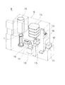
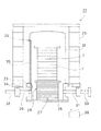
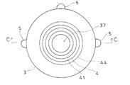
【解決手段】基板7を処理する反応炉と、該反応炉内で基板7を保持する基板保持具1と、基板保持具1内に設けられ、基板7と接触するリング状の支持板4と、支持板4と異なる材質で形成された支持板4を載置する補助支持板3とを具備し、支持板4の裏面に凹部39を形成し、補助支持板3には凹部39に嵌合する凸部38を設けた。
【選択図】図4
Description
又、本発明は以下の実施の態様を含む。
の基板処理装置。
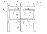
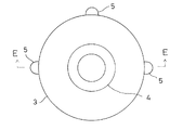
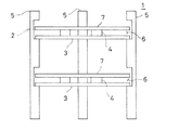
3 補助支持板
4 支持板
7 ウェーハ
8 基板処理装置
37 貫通孔
38 環状凸部
39 環状凹部
41 支持突起
42 平面
43 内嵌凸部
44 外嵌凸部
45 位置決め凸部
46 座刳
Claims (1)
- 基板を処理する反応炉と、該反応炉内で基板を保持する基板保持具と、該基板保持具内に設けられ、前記基板と接触するリング状の支持板と、該支持板と異なる材質で形成された前記支持板を載置する補助支持板とを具備し、前記支持板の裏面に凹部を形成し、前記補助支持板には前記凹部に嵌合する凸部を設けたことを特徴とする基板処理装置。
Priority Applications (1)
| Application Number | Priority Date | Filing Date | Title |
|---|---|---|---|
| JP2008317228A JP2010141202A (ja) | 2008-12-12 | 2008-12-12 | 基板処理装置 |
Applications Claiming Priority (1)
| Application Number | Priority Date | Filing Date | Title |
|---|---|---|---|
| JP2008317228A JP2010141202A (ja) | 2008-12-12 | 2008-12-12 | 基板処理装置 |
Publications (2)
| Publication Number | Publication Date |
|---|---|
| JP2010141202A true JP2010141202A (ja) | 2010-06-24 |
| JP2010141202A5 JP2010141202A5 (ja) | 2012-01-26 |
Family
ID=42351059
Family Applications (1)
| Application Number | Title | Priority Date | Filing Date |
|---|---|---|---|
| JP2008317228A Pending JP2010141202A (ja) | 2008-12-12 | 2008-12-12 | 基板処理装置 |
Country Status (1)
| Country | Link |
|---|---|
| JP (1) | JP2010141202A (ja) |
Cited By (1)
| Publication number | Priority date | Publication date | Assignee | Title |
|---|---|---|---|---|
| CN110890309A (zh) * | 2018-09-10 | 2020-03-17 | 桦榆国际有限公司 | 石墨盘修补方法 |
Citations (5)
| Publication number | Priority date | Publication date | Assignee | Title |
|---|---|---|---|---|
| JPH09186228A (ja) * | 1995-12-28 | 1997-07-15 | Samsung Electron Co Ltd | ウェーハ支持装置 |
| JP2003031647A (ja) * | 2001-07-19 | 2003-01-31 | Hitachi Kokusai Electric Inc | 基板処理装置および半導体装置の製造方法 |
| JP2005012058A (ja) * | 2003-06-20 | 2005-01-13 | Sumitomo Mitsubishi Silicon Corp | 半導体基板の熱処理ボートおよび熱処理方法 |
| JP2006093283A (ja) * | 2004-09-22 | 2006-04-06 | Sumco Corp | ウェーハ支持具 |
| JP2008300374A (ja) * | 2007-05-29 | 2008-12-11 | Shin Etsu Chem Co Ltd | 静電吸着装置 |
-
2008
- 2008-12-12 JP JP2008317228A patent/JP2010141202A/ja active Pending
Patent Citations (5)
| Publication number | Priority date | Publication date | Assignee | Title |
|---|---|---|---|---|
| JPH09186228A (ja) * | 1995-12-28 | 1997-07-15 | Samsung Electron Co Ltd | ウェーハ支持装置 |
| JP2003031647A (ja) * | 2001-07-19 | 2003-01-31 | Hitachi Kokusai Electric Inc | 基板処理装置および半導体装置の製造方法 |
| JP2005012058A (ja) * | 2003-06-20 | 2005-01-13 | Sumitomo Mitsubishi Silicon Corp | 半導体基板の熱処理ボートおよび熱処理方法 |
| JP2006093283A (ja) * | 2004-09-22 | 2006-04-06 | Sumco Corp | ウェーハ支持具 |
| JP2008300374A (ja) * | 2007-05-29 | 2008-12-11 | Shin Etsu Chem Co Ltd | 静電吸着装置 |
Cited By (2)
| Publication number | Priority date | Publication date | Assignee | Title |
|---|---|---|---|---|
| CN110890309A (zh) * | 2018-09-10 | 2020-03-17 | 桦榆国际有限公司 | 石墨盘修补方法 |
| CN110890309B (zh) * | 2018-09-10 | 2023-09-08 | 桦榆国际有限公司 | 石墨盘修补方法 |
Similar Documents
| Publication | Publication Date | Title |
|---|---|---|
| US8012888B2 (en) | Substrate processing apparatus and semiconductor device manufacturing method | |
| CN101714504B (zh) | 热处理装置、半导体装置的制造方法及衬底的制造方法 | |
| JP4815352B2 (ja) | 熱処理装置、基板の製造方法、基板処理方法、及び半導体装置の製造方法 | |
| JP2010141202A (ja) | 基板処理装置 | |
| JP4700300B2 (ja) | 熱処理装置 | |
| JP2005101161A (ja) | 熱処理用支持具、熱処理装置、熱処理方法、基板の製造方法及び半導体装置の製造方法 | |
| JP2007073865A (ja) | 熱処理装置 | |
| JP2006080294A (ja) | 基板の製造方法 | |
| JP2009016532A (ja) | 基板処理装置及び半導体装置の製造方法 | |
| JP2006100303A (ja) | 基板の製造方法及び熱処理装置 | |
| JP4611229B2 (ja) | 基板支持体、基板処理装置、基板処理方法、基板の製造方法、及び半導体装置の製造方法 | |
| JP2005086132A (ja) | 熱処理装置、半導体装置の製造方法、基板の製造方法及び基板処理方法 | |
| JP2004356355A (ja) | 熱処理方法、基板の製造方法、半導体装置の製造方法及び熱処理装置 | |
| JP2004281669A (ja) | 熱処理装置 | |
| JP5010884B2 (ja) | 基板処理装置、基板搬送方法および半導体集積回路装置の製造方法 | |
| JP2008078427A (ja) | 熱処理装置 | |
| JP2009088395A (ja) | 基板処理装置 | |
| JP2011176320A (ja) | 基板処理装置 | |
| JP2008028306A (ja) | 熱処理装置 | |
| JP2009147383A (ja) | 熱処理方法 | |
| JP2007134518A (ja) | 熱処理装置 | |
| JP2010010280A (ja) | 基板処理装置 | |
| JP2008078459A (ja) | 基板処理装置 | |
| JP2005064367A (ja) | 熱処理装置、半導体装置の製造方法、基板の製造方法及び基板処理方法 | |
| JP2006261317A (ja) | 熱処理装置及び基板の製造方法 |
Legal Events
| Date | Code | Title | Description |
|---|---|---|---|
| A521 | Written amendment |
Effective date: 20111206 Free format text: JAPANESE INTERMEDIATE CODE: A523 |
|
| A621 | Written request for application examination |
Free format text: JAPANESE INTERMEDIATE CODE: A621 Effective date: 20111206 |
|
| A977 | Report on retrieval |
Free format text: JAPANESE INTERMEDIATE CODE: A971007 Effective date: 20121206 |
|
| A131 | Notification of reasons for refusal |
Effective date: 20121211 Free format text: JAPANESE INTERMEDIATE CODE: A131 |
|
| A02 | Decision of refusal |
Effective date: 20130409 Free format text: JAPANESE INTERMEDIATE CODE: A02 |