JP2010141202A - Substrate processing apparatus - Google Patents
Substrate processing apparatus Download PDFInfo
- Publication number
- JP2010141202A JP2010141202A JP2008317228A JP2008317228A JP2010141202A JP 2010141202 A JP2010141202 A JP 2010141202A JP 2008317228 A JP2008317228 A JP 2008317228A JP 2008317228 A JP2008317228 A JP 2008317228A JP 2010141202 A JP2010141202 A JP 2010141202A
- Authority
- JP
- Japan
- Prior art keywords
- support plate
- substrate
- wafer
- auxiliary support
- pod
- Prior art date
- Legal status (The legal status is an assumption and is not a legal conclusion. Google has not performed a legal analysis and makes no representation as to the accuracy of the status listed.)
- Pending
Links
- 239000000758 substrate Substances 0.000 title claims abstract description 98
- 238000006243 chemical reaction Methods 0.000 claims abstract description 53
- 239000000463 material Substances 0.000 claims abstract description 9
- 238000000034 method Methods 0.000 abstract description 17
- 238000006073 displacement reaction Methods 0.000 abstract description 3
- 235000012431 wafers Nutrition 0.000 description 77
- 239000007789 gas Substances 0.000 description 21
- HBMJWWWQQXIZIP-UHFFFAOYSA-N silicon carbide Chemical compound [Si+]#[C-] HBMJWWWQQXIZIP-UHFFFAOYSA-N 0.000 description 17
- 238000010438 heat treatment Methods 0.000 description 14
- XUIMIQQOPSSXEZ-UHFFFAOYSA-N Silicon Chemical compound [Si] XUIMIQQOPSSXEZ-UHFFFAOYSA-N 0.000 description 10
- 229910052710 silicon Inorganic materials 0.000 description 10
- 239000010703 silicon Substances 0.000 description 10
- 238000004519 manufacturing process Methods 0.000 description 9
- 229910010271 silicon carbide Inorganic materials 0.000 description 9
- VYPSYNLAJGMNEJ-UHFFFAOYSA-N silicon dioxide Inorganic materials O=[Si]=O VYPSYNLAJGMNEJ-UHFFFAOYSA-N 0.000 description 7
- 239000002245 particle Substances 0.000 description 6
- 239000010408 film Substances 0.000 description 5
- 230000003647 oxidation Effects 0.000 description 5
- 238000007254 oxidation reaction Methods 0.000 description 5
- 229910052760 oxygen Inorganic materials 0.000 description 5
- 239000004065 semiconductor Substances 0.000 description 5
- 235000012239 silicon dioxide Nutrition 0.000 description 5
- UFHFLCQGNIYNRP-UHFFFAOYSA-N Hydrogen Chemical compound [H][H] UFHFLCQGNIYNRP-UHFFFAOYSA-N 0.000 description 4
- 239000001257 hydrogen Substances 0.000 description 4
- 229910052739 hydrogen Inorganic materials 0.000 description 4
- 229910052751 metal Inorganic materials 0.000 description 4
- 239000002184 metal Substances 0.000 description 4
- 239000001301 oxygen Substances 0.000 description 4
- QVGXLLKOCUKJST-UHFFFAOYSA-N atomic oxygen Chemical compound [O] QVGXLLKOCUKJST-UHFFFAOYSA-N 0.000 description 3
- 238000009792 diffusion process Methods 0.000 description 3
- 239000012535 impurity Substances 0.000 description 3
- 230000002093 peripheral effect Effects 0.000 description 3
- 239000010453 quartz Substances 0.000 description 3
- 239000010409 thin film Substances 0.000 description 3
- 230000032258 transport Effects 0.000 description 3
- XKRFYHLGVUSROY-UHFFFAOYSA-N Argon Chemical compound [Ar] XKRFYHLGVUSROY-UHFFFAOYSA-N 0.000 description 2
- 238000000137 annealing Methods 0.000 description 2
- 229910052786 argon Inorganic materials 0.000 description 2
- 229910052681 coesite Inorganic materials 0.000 description 2
- 229910052906 cristobalite Inorganic materials 0.000 description 2
- 239000013078 crystal Substances 0.000 description 2
- 238000005530 etching Methods 0.000 description 2
- 238000009434 installation Methods 0.000 description 2
- 239000010410 layer Substances 0.000 description 2
- -1 oxygen ions Chemical class 0.000 description 2
- 239000000377 silicon dioxide Substances 0.000 description 2
- 229910052682 stishovite Inorganic materials 0.000 description 2
- 229910052905 tridymite Inorganic materials 0.000 description 2
- IJGRMHOSHXDMSA-UHFFFAOYSA-N Atomic nitrogen Chemical compound N#N IJGRMHOSHXDMSA-UHFFFAOYSA-N 0.000 description 1
- ZOXJGFHDIHLPTG-UHFFFAOYSA-N Boron Chemical compound [B] ZOXJGFHDIHLPTG-UHFFFAOYSA-N 0.000 description 1
- OAICVXFJPJFONN-UHFFFAOYSA-N Phosphorus Chemical compound [P] OAICVXFJPJFONN-UHFFFAOYSA-N 0.000 description 1
- 229910052787 antimony Inorganic materials 0.000 description 1
- WATWJIUSRGPENY-UHFFFAOYSA-N antimony atom Chemical compound [Sb] WATWJIUSRGPENY-UHFFFAOYSA-N 0.000 description 1
- 229910052785 arsenic Inorganic materials 0.000 description 1
- RQNWIZPPADIBDY-UHFFFAOYSA-N arsenic atom Chemical compound [As] RQNWIZPPADIBDY-UHFFFAOYSA-N 0.000 description 1
- 230000015572 biosynthetic process Effects 0.000 description 1
- 229910052796 boron Inorganic materials 0.000 description 1
- 238000002485 combustion reaction Methods 0.000 description 1
- 238000011109 contamination Methods 0.000 description 1
- 230000007423 decrease Effects 0.000 description 1
- 230000007547 defect Effects 0.000 description 1
- 239000002019 doping agent Substances 0.000 description 1
- 238000005553 drilling Methods 0.000 description 1
- 239000011521 glass Substances 0.000 description 1
- 239000012212 insulator Substances 0.000 description 1
- 238000005468 ion implantation Methods 0.000 description 1
- 238000002844 melting Methods 0.000 description 1
- 230000008018 melting Effects 0.000 description 1
- 229910021421 monocrystalline silicon Inorganic materials 0.000 description 1
- 229910052698 phosphorus Inorganic materials 0.000 description 1
- 239000011574 phosphorus Substances 0.000 description 1
- 230000002265 prevention Effects 0.000 description 1
- 230000001698 pyrogenic effect Effects 0.000 description 1
- 238000007789 sealing Methods 0.000 description 1
- 238000000926 separation method Methods 0.000 description 1
- 239000002344 surface layer Substances 0.000 description 1
- 238000002230 thermal chemical vapour deposition Methods 0.000 description 1
- 238000009279 wet oxidation reaction Methods 0.000 description 1
Images


Landscapes
- Container, Conveyance, Adherence, Positioning, Of Wafer (AREA)
Abstract
【課題】SiC製補助支持板とSi製支持板との間の位置ずれによって発生する基板間の膜の不均一を防止する基板処理装置を提供する。
【解決手段】基板7を処理する反応炉と、該反応炉内で基板7を保持する基板保持具1と、基板保持具1内に設けられ、基板7と接触するリング状の支持板4と、支持板4と異なる材質で形成された支持板4を載置する補助支持板3とを具備し、支持板4の裏面に凹部39を形成し、補助支持板3には凹部39に嵌合する凸部38を設けた。
【選択図】図4Provided is a substrate processing apparatus for preventing non-uniformity of a film between substrates caused by displacement between a SiC auxiliary support plate and a Si support plate.
A reaction furnace that processes a substrate, a substrate holder that holds the substrate in the reaction furnace, a ring-shaped support plate that is provided in the substrate holder and contacts the substrate, and And an auxiliary support plate 3 on which the support plate 4 made of a material different from that of the support plate 4 is placed. A recess 39 is formed on the back surface of the support plate 4, and the auxiliary support plate 3 is fitted into the recess 39. Protruding portions 38 are provided.
[Selection] Figure 4
Description
本発明は、シリコンウェーハ、ガラス基板等の基板に、薄膜を生成し、或は不純物の拡散、エッチング、アニール処理等の処理を行う基板処理装置に関するものである。 The present invention relates to a substrate processing apparatus that forms a thin film on a substrate such as a silicon wafer or a glass substrate, or performs processing such as impurity diffusion, etching, and annealing.
シリコンウェーハ等の基板から半導体装置を製造する工程に、熱CVD法による薄膜の生成、不純物の拡散、エッチング、熱処理等の基板処理が有り、斯かる基板処理を行うものとして基板処理装置がある。 The process of manufacturing a semiconductor device from a substrate such as a silicon wafer includes substrate processing such as thin film formation, impurity diffusion, etching, and heat treatment by thermal CVD, and there is a substrate processing apparatus that performs such substrate processing.
基板処理をする際には、ウェーハを載置した基板保持具(以下、ボートと称す)を反応炉内に装入し、各種処理ガスを導入して各処理を行う。 When performing substrate processing, a substrate holder (hereinafter referred to as a boat) on which a wafer is placed is placed in a reaction furnace, and various processing gases are introduced to perform each processing.
又、従来、前記基板処理装置を用いて複数枚のウェーハを熱処理する場合、前記ボートの支柱に設けられた炭化珪素(SiC)製補助支持板載置部にSiC製の補助支持板を載置し、該補助支持板上にシリコン(Si)製の支持板を載置し、該Si製の支持板上に処理すべきウェーハを載置していた。 Conventionally, when heat-treating a plurality of wafers using the substrate processing apparatus, an SiC auxiliary support plate is placed on a silicon carbide (SiC) auxiliary support plate placement portion provided on the column of the boat. Then, a support plate made of silicon (Si) was placed on the auxiliary support plate, and a wafer to be processed was placed on the support plate made of Si.
図11、図12に於いて、従来のウェーハ載置方法について説明する。 A conventional wafer mounting method will be described with reference to FIGS.
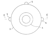
ボート1は、本体部2と補助支持部としての補助支持板3、支持部としてのリング状の支持板4から構成されている。前記本体部2は、炭化珪素(SiC)又はシリコンを含浸させた炭化珪素から成り、図示しない円盤状の上板、図示しない円盤状の下板、及び前記上板と前記下板を接続する例えば3本の支柱5を有する。該支柱5は互いに90度ずつ隔てて配設され、図示しないツイーザが両端の前記支柱5,5間に挿入可能となっている。又、前記補助支持板3を載置する為の溝部6が垂直方向に一定間隔を隔てて水平に多数形成されている。前記補助支持板3は炭化珪素(SiC)又はシリコンを含浸させた炭化珪素から成り、前記支柱5に形成されている各溝部6で溝数と同数支持される。又前記支持板4は、前記補助支持板3の同心となる様該補助支持板3の上面に設置され、ウェーハ7は下面が前記支持板4の上面と当接し、支持されている。該支持板4は、例えばシリコン(Si)製の板状部材から成り、円筒形状に形成されている。又、該支持板4の径は前記ウェーハ7よりも小さく、該ウェーハ7はウェーハ周縁部と接触することなく前記支持板4に支持される。
The
尚、該支持板4の径は、ウェーハ7を前記支持板4に載置した際に、ウェーハ7との接触部よりも外側のウェーハ7の面積と、前記接触部よりも内側のウェーハ7の面積が等しくなる様な径が望ましい。
The diameter of the
然し乍ら、上記の構成で熱処理をした場合、熱処理中に前記支持板4から金属原子が放出され、該金属原子がウェーハ7に付着してウェーハ7の歩留りを減少させる問題や、前記補助支持板3と該補助支持板3の上に載置される前記支持板4の間には位置ずれ防止機構がなく、昇温時の前記支持板4と前記補助支持板3との熱膨張率が違う為、前記支持板4と前記補助支持板3との間に位置ずれが発生し、ウェーハ7間の膜の均一性が悪くなる問題や、ウェーハ7と該ウェーハ7を支持している前記支持板4との間に熱膨張による摩擦が生じ、パーティクルが発生し、該パーティクルが前記ウェーハ7に付着し、該ウェーハ7の歩留りを低下させる問題等があった。
However, when heat treatment is performed with the above-described configuration, metal atoms are released from the
尚、ボートバー長手方向側面から先端を垂直に突設させた接触部を設け、該接触部がウェーハを裏面から支持する機構を持つウェーハ支持装置として、特許文献1に示されるものがある。
As a wafer support device having a mechanism in which a contact portion having a tip projecting vertically from a side surface in the longitudinal direction of the boat bar is provided and the contact portion supports a wafer from the back surface, there is one disclosed in
本発明は斯かる実情に鑑み、SiC製補助支持板とSi製支持板との間の位置ずれによって発生する基板間の膜の不均一を防止する基板処理装置を提供するものである。 In view of such circumstances, the present invention provides a substrate processing apparatus that prevents non-uniformity of a film between substrates caused by a displacement between a SiC auxiliary support plate and a Si support plate.
本発明は、基板を処理する反応炉と、該反応炉内で基板を保持する基板保持具と、該基板保持具内に設けられ、前記基板と接触するリング状の支持板と、該支持板と異なる材質で形成された前記支持板を載置する補助支持板とを具備し、前記支持板の裏面に凹部を形成し、前記補助支持板には前記凹部に嵌合する凸部を設けた基板処理装置に係るものである。 The present invention includes a reaction furnace for processing a substrate, a substrate holder for holding the substrate in the reaction furnace, a ring-shaped support plate provided in the substrate holder and in contact with the substrate, and the support plate And an auxiliary support plate on which the support plate formed of a different material is placed, and a concave portion is formed on the back surface of the support plate, and a convex portion that fits into the concave portion is provided on the auxiliary support plate. The present invention relates to a substrate processing apparatus.
本発明によれば、基板を処理する反応炉と、該反応炉内で基板を保持する基板保持具と、該基板保持具内に設けられ、前記基板と接触するリング状の支持板と、該支持板と異なる材質で形成された前記支持板を載置する補助支持板とを具備し、前記支持板の裏面に凹部を形成し、前記補助支持板には前記凹部に嵌合する凸部を設けたので、前記支持板と前記補助支持板の位置ずれを防止し、前記基板間の膜の均一性の向上を図るという優れた効果を発揮する。 According to the present invention, a reaction furnace for processing a substrate, a substrate holder for holding the substrate in the reaction furnace, a ring-shaped support plate provided in the substrate holder and in contact with the substrate, An auxiliary support plate on which the support plate formed of a material different from that of the support plate is placed, a recess is formed on the back surface of the support plate, and a convex portion that fits into the recess is formed on the auxiliary support plate. Since it is provided, it is possible to prevent the positional deviation between the support plate and the auxiliary support plate and to improve the film uniformity between the substrates.
以下、図面を参照しつつ本発明を実施する為の最良の形態を説明する。 The best mode for carrying out the present invention will be described below with reference to the drawings.
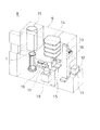
先ず、図1に於いて、本発明が実施される基板処理装置8の構成について説明する。
First, referring to FIG. 1, the configuration of a
該基板処理装置8は、バッチ式縦型基板処理装置であり、主要部が配置される筐体9を有する。該筐体9の正面側には、ポッドステージ11が接続されており、該ポッドステージ11にポッド12が搬送される。該ポッド12には、例えば25枚の被処理基板としてのウェーハ7が収納され、図示しない蓋が閉じられた状態で前記ポッドステージ11にセットされている。
The
前記筐体9内の正面側であって、前記ポッドステージ11に対向する位置には、ポッド搬送装置13が配置されている。又、該ポッド搬送装置13の近傍には、ポッド棚14、ポッドオープナ15、及び基板枚数検知器16が配置されている。前記ポッド棚14は前記ポッドオープナ15の上方に配置され、前記基板枚数検知器16は前記ポッドオープナ15に隣接して配置される。前記ポッド搬送装置13は、前記ポッドステージ11と前記ポッド棚14と前記ポッドオープナ15との間で前記ポッド12を搬送する。前記ポッドオープナ15は前記ポッド12の蓋を開けるものであり、該蓋が開けられた前記ポッド12内のウェーハ7の枚数が前記基板枚数検知器16により検知される。
A
更に、前記筐体9内には、基板移載機17、ノッチアライナ18、及びボート(基板保持具)1が配置されている。前記基板移載機17は、例えば5枚のウェーハ7を取出すことができるツイーザ(アーム)19を有しており、該ツイーザ19を動かすことで、前記ポッドオープナ15の位置におかれた前記ポッド12、前記ノッチアライナ18、及び前記ボート1間でウェーハ7を搬送する。前記ノッチアライナ18は、ウェーハ7に形成されたノッチ又はオリフラを検出し、ウェーハ7のノッチ又はオリフラを一定の位置に揃えるものである。
Further, a
更に、前記筐体9内の背面側上部には、反応炉21が配置されている。該反応炉21内に、複数枚のウェーハ7を装填した前記ボート1が装入され、熱処理が行われる。
Further, a
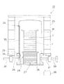
次に、図2に於いて、前記反応炉21の一例を示す。
Next, an example of the
該反応炉21は、炭化珪素(SiC)製の反応管22を有する。該反応管22は、上端部が閉塞され、下端部が開放された円筒形状であり、開放された下端部にはフランジが形成されている。前記反応管22の下方には石英製のアダプタ23が配置され、該アダプタ23は上端部と下端部が開放された円筒形状であり、開放された上端部と下端部にはフランジが形成され、前記反応管22の下端部フランジは前記アダプタ23の上端部フランジと当接して支持されている。前記反応管22と前記アダプタ23により反応容器24が形成され、該反応容器24のうち、前記アダプタ23を除いた前記反応管22の周囲にはヒータ25が配設されている。
The
前記反応容器24下部は、前記ボート1を挿入する為に開放され、この開放部分(炉口部)は炉口シールキャップ26がOリングを挾んで前記アダプタ23の下端部フランジの下面に当接することにより密閉される様にしている。前記炉口シールキャップ26は前記ボート1を支持し、該ボート1と共に昇降可能に設けられている。又、前記炉口シールキャップ26と前記ボート1との間には、石英製の第1の断熱部材27と、該第1の断熱部材27の上部に配置された炭化珪素(SiC)製の第2の断熱部材28とが設けられている。前記ボート1は、多数枚、例えば25〜100枚のウェーハ7を略水平状態で隙間をもって多段に支持し、前記反応管22内に装填される。
The lower portion of the
1200℃以上の高温での処理を可能とする為、前記反応管22は炭化珪素(SiC)製としてある。該反応管22を炉口部迄延し、該炉口部をOリングを介して前記炉口シールキャップ26でシールする構造とすると、前記SiC製の反応管22を介して伝達された熱によりシール部迄高温となり、シール材料であるOリングを溶かしてしまう虞れがある。又、Oリングを溶かさない様に前記反応管22のシール部を冷却すると、温度差による熱膨張で破損してしまう。そこで、前記反応容器24のうち、前記ヒータ25による加熱領域を前記反応管22で構成し、加熱領域から外れた部分を前記石英製のアダプタ23で構成することで、前記反応管22からの熱の伝達を和らげ、Oリングを溶かすことなく、又前記反応管22を破損することなく炉口部をシールすることが可能となる。又、前記反応管22と前記アダプタ23とのシールは、双方の面精度をよくすれば前記反応管22は前記ヒータ25の加熱領域に配置されている為温度差が発生せず、等方的に熱膨張する。従って、前記反応管22の下端部フランジを平面に保つことができ、前記アダプタ23との間に隙間ができないので、前記反応管22を前記アダプタ23に載せるだけでシール性を確保することができる。
In order to enable processing at a high temperature of 1200 ° C. or higher, the
前記アダプタ23には、該アダプタ23と一体にガス供給口29とガス排気口31が設けられており、前記ガス供給口29にはガス導入管32が接続され、前記ガス排気口31にはガス排気管33が接続されている。
The
前記アダプタ23の内壁は前記反応管22の内壁よりも内側に突出しており、前記アダプタ23の側壁部には、前記ガス供給口29と連通し、垂直方向に向かうガス導入経路34が設けられ、該ガス導入経路34の上部にはノズル取付孔が上方に開口する様に設けられている。該ノズル取付孔は、前記反応管22の内部に於ける前記アダプタ23の上端部フランジの上面に開口しており、前記ガス供給口29及び前記ガス導入経路34と連通し、又前記ノズル取付孔にはノズル35が挿入され、固定されている。即ち、前記反応管22の内壁よりも内側に突出した前記アダプタ23の上面に前記ノズル35が接続され、又該ノズル35は前記アダプタ23によって支持される。
The inner wall of the
上記構成により、ノズル接続部は熱で変形し難く、破損し難い。又、前記ノズル35と前記アダプタ23の組立てや解体が容易になる。前記ガス導入管32から前記ガス供給口29に導入された処理ガスは、前記アダプタ23の側壁部に設けられた前記ガス導入経路34、前記ノズル35を介して前記反応管22内に供給される、尚、前記ノズル35は前記反応管22の内壁に沿って基板配列領域の上端よりも上方、即ち前記ボート1の上端よりも上方迄延びる様に構成される。
With the above configuration, the nozzle connecting portion is hardly deformed by heat and is not easily damaged. Further, the
次に、上述した様に構成された基板処理装置8の作用について説明する。尚、以下の説明に於いて、前記基板処理装置8を構成する各部の動作はコントローラ36によって制御される。
Next, the operation of the
先ず、前記ポッドステージ11に複数枚のウェーハ7を収容した前記ポッド12がセットされると、前記ポッド搬送装置13により前記ポッド12を前記ポッドステージ11から前記ポッド棚14へ搬送し、収納する。次に、前記ポッド搬送装置13が前記ポッド12を前記ポッドオープナ15に搬送、セットし、該ポッドオープナ15が前記ポッド12の蓋を開き、前記基板枚数検知器16により前記ウェーハ7の枚数を検知する。
First, when the
次に、前記基板移載機17により、前記ポッドオープナ15の位置にある前記ポッド12から前記ウェーハ7を取出し、前記ノッチアライナ18に移載する。該ノッチアライナ18は、前記ウェーハ7を回転させながらノッチを検出し、検出した情報に基づいて複数枚の前記ウェーハ7のノッチを同じ位置に整列させる。整列させた前記ウェーハ7を前記基板移載機17により前記ノッチアライナ18から取出し、前記ボート1に移載する。
Next, the
上記の様に、1バッチ分の前記ウェーハ7を前記ボート1に移載すると、例えば600℃程度の温度に設定された前記反応炉21(反応容器24)内に複数枚のウェーハ7を装填したまま前記ボート1を装入し、前記炉口シールキャップ26により前記反応炉21を密閉する。次に、炉内温度を熱処理温度迄昇温させ、前記ガス導入管32から前記ガス供給口29、前記アダプタ23側壁部に設けられた前記ガス導入経路34及びノズル35を介して前記反応管22内に処理ガスを導入する。処理ガスには、窒素(N2 )、アルゴン(Ar)、水素(H2 )、酸素(O2 )等が含まれる。前記ウェーハ7を熱処理する際、該ウェーハ7は例えば1200℃程度以上の温度に加熱される。
As described above, when one batch of the
該ウェーハ7の熱処理が終了すると、例えば炉内温度を600℃程度の温度に降温した後、前記ウェーハ7を支持した前記ボート1を前記反応炉21から払出し、前記ウェーハ7が冷える迄所定の場所で待機させる。該ウェーハ7が所定温度迄冷却されると、前記基板移載機17により、前記ボート1から前記ウェーハ7を取出し、前記ポッドオープナ15にセットされている空の前記ポッド12に搬送して収容する。最後に、前記ポッド搬送装置13により、前記ポッド棚14又は前記ポッドステージ11に搬出し、一連の処理が完了する。
When the heat treatment of the
次に、図3、図4に於いて、本発明の第1の実施の形態のボート1について説明する。尚、図3、図4中、図11、図12と同等のものには同符号を付し、その説明を省略する。
Next, with reference to FIGS. 3 and 4, the
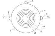
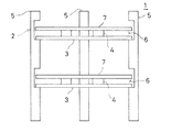
ボート1は、本体部2と補助支持部としての補助支持板3、支持部としてのリング状の支持板4から構成されている。前記本体部2は、炭化珪素(SiC)又はシリコンを含浸させた炭化珪素から成り、図示しない円盤状の上板、図示しない円盤状の下板、及び前記上板と前記下板を接続する例えば3本の支柱5を有する。該支柱5は互いに90度ずつ隔てて配設され、ツイーザ19及び該ツイーザ19に載置されたウェーハ7を、両端の前記支柱5,5間に挿入可能となっている。又、前記補助支持板3を載置する為の溝部6が垂直方向に一定間隔を隔てて水平に多数形成されている。前記補助支持板3は炭化珪素(SiC)又はシリコンを含浸させた炭化珪素から成り、前記支柱5に形成されている各溝部6で溝数と同数支持される。
The
前記補助支持板3の中心部には貫通孔37が穿設されており、前記補助支持板3の上面には、例えばリング状で前記支持板4の幅よりも小さな幅の環状凸部38が設けられている。
A through-
又、前記支持板4は、前記補助支持板3の同心となる様該補助支持板3の上面に設置され、前記支持板4の下面には前記環状凸部38が嵌合可能で、該環状凸部38を嵌合した際に、半径方向と上方向に前記補助支持板3と前記支持板4の熱膨張差を吸収できるだけの隙間を有する環状凹部39が設けられている。前記支持板4は下端面の面積よりも上端面の面積が小さく形成され、上部に支持突起41が突設され、該支持突起41の内周側及び外周側に平面42が形成された凸形状であり、ウェーハ7は下面が前記支持突起41と当接し、支持されている。前記支持板4は、例えばシリコン(Si)製の板状部材から成り、リング状に形成されている。又、該支持板4の径は前記ウェーハ7よりも小さく、該ウェーハ7はウェーハ周縁部と接触することなく前記支持板4に支持される。
The
尚、前記貫通孔37の径は、前記支持板4の内径と同じか、該支持板4の内径よりも小さいものとし、又、該支持板4の形状は上面の面積が下面の面積よりも小さければよいので、断面積が台形、或はL字形状であってもよい。
The diameter of the through
前記ツイーザ19に載置されたウェーハ7を前記支持突起41に移載し、前記ボート1を反応炉21に装入して基板処理をする際には、前記貫通孔37を穿設して前記補助支持板3の面積を減少させたことで、該補助支持板3から放出される金属原子の量を減少させ、ウェーハ7への金属汚染量を低減することができる。
When the
又、前記環状凸部38を前記環状凹部39に嵌合させることにより、SiC製の前記補助支持板3と、Si製の前記支持板4の材質の違いによる熱膨張率の差により発生する位置ずれを防止し、ウェーハ7の膜の均一性を改善できる。
Further, by fitting the annular
又、前記支持突起41にウェーハ7を載置し、該ウェーハ7と前記支持板4との接触面積を小さくすることで、熱膨張により前記ウェーハ7と前記支持板4の間の摩擦によって発生するパーティクルを低減し、又前記支持板4を凸形状としたので、発生したパーティクルは前記支持突起41の脇から落下して前記平面42に堆積し、ウェーハ7に対するパーティクルの付着を防ぎ、ウェーハ7の歩留りを増加させることができる。
Further, by placing the
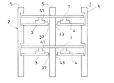
次に、図5、図6に於いて、本発明の第2の実施の形態について説明する。尚、図5、図6中、図3、図4と同等のものには同符号を付し、その説明を省略する。 Next, a second embodiment of the present invention will be described with reference to FIGS. In FIGS. 5 and 6, the same components as those in FIGS. 3 and 4 are denoted by the same reference numerals, and description thereof is omitted.
第2の実施の形態は、第1の実施の形態に於ける補助支持板3の環状凸部38と支持板4の環状凹部39を取除いたものであり、補助支持板3に貫通孔37を穿設し、該貫通孔37の円縁部にリング状で連続した内嵌凸部43を設けたものである。該内嵌凸部43の外径は前記補助支持板3の上面に設置されているリング状の支持板4の内径よりも加熱により発生する熱膨張差を吸収する為の隙間分だけ小さい径を外径としたものである。
In the second embodiment, the annular
前記支持板4の内径部に前記内嵌凸部43を嵌合させることにより、前記支持板4を固定することができ、基板処理を行う際には、前記補助支持板3と前記支持板4の熱膨張によって発生する位置ずれを防止できる。
The
又、第2の実施の形態に於ける前記補助支持板3及び前記支持板4の設置方法は、前記補助支持板3のみの形状変更で実現可能な為、部品の交換や改造を行う際のコスト低減を図ることができる。
Moreover, since the installation method of the
尚、前記内嵌凸部43は、連続せずに前記貫通孔37の円周部に所定の間隔で断続的に突設したものであってもよい。
In addition, the said internal fitting
次に図7、図8に於いて、本発明の第3の実施の形態について説明する。尚、図7、図8中、図3、図4と同等のものには同符号を付し、その説明を省略する。 Next, a third embodiment of the present invention will be described with reference to FIGS. 7 and 8, the same components as those in FIGS. 3 and 4 are denoted by the same reference numerals, and the description thereof is omitted.
第3の実施の形態は、第2の実施の形態に於ける補助支持板3の内嵌凸部43を取除き、代りに支持板4と同心円状にリング状で連続した外嵌凸部44を設けたものである。該外嵌凸部44の内径は、前記補助支持板3の上面に設置されているリング状の前記支持板4の外径より加熱により発生する熱膨張差を吸収する為の隙間分だけ大きい径を内径としたものである。
In the third embodiment, the inner fitting
前記支持板4の外径部に前記外嵌凸部44を嵌合させることにより、前記支持板4を固定することができ、基板処理を行う際には、前記補助支持板3と前記支持板4の熱膨張によって発生する位置ずれを防止できる。
By fitting the outer fitting
又、第3の実施の形態に於ける前記補助支持板3及び前記支持板4の設置方法は、前記補助支持板3のみの形状変更で実現可能な為、部品の交換や改造を行う際のコスト低減を図ることができる。
Moreover, since the installation method of the
尚、前記外嵌凸部44は、連続せずに前記支持板4の外径よりも僅かに大きい同心円状に所定の間隔で断続的に突設したものであってもよい。
In addition, the said external fitting
次に、図9、図10に於いて、本発明の第4の実施の形態について説明する。尚、図9、図10中、図3、図4と同等のものには同符号を付し、その説明を省略する。 Next, a fourth embodiment of the present invention will be described with reference to FIGS. In FIG. 9 and FIG. 10, parts that are the same as those in FIG. 3 and FIG.
第4の実施の形態は、第1の実施の形態に於ける環状凸部38の代りにリング状の支持板4と同心の円周上に円柱や方柱等の形状の位置決め凸部45を複数個、例えば円周に対して等分の位置になる様に設け、環状凹部39の代りに前記位置決め凸部45を収納可能で、該位置決め凸部45を収納した際には、径方向と上方向に補助支持板3と前記支持板4の熱膨張差を吸収できるだけの隙間を有する座刳46を設けたものである。
In the fourth embodiment, instead of the annular
前記位置決め凸部45を前記座刳46に収納し、固定することで、SiC製の前記補助支持板3と、Si製の前記支持板4の材質の違いによる熱膨張率の差により発生する位置ずれを防止し、ウェーハ7の膜の均一性の向上を図ることができる。
The position generated by the difference in thermal expansion coefficient due to the difference in material between the
尚、上記実施の形態の説明に於いては、一度に複数枚のウェーハ7を処理するバッチ式の基板処理装置を用いたが、本発明はこれに限定されるものではなく、枚葉式のものであってもよい。
In the description of the above embodiment, a batch type substrate processing apparatus for processing a plurality of
又、本発明の基板処理装置は、基板の製造工程にも適用することができる。 The substrate processing apparatus of the present invention can also be applied to a substrate manufacturing process.
SOI(Silicon On Insulator)ウェーハの一種であるSIMOX(Separation by Implanted Oxygen)ウェーハの製造工程の一工程に本発明の基板処理装置を適用する例について説明する。 An example in which the substrate processing apparatus of the present invention is applied to one process of manufacturing a SIMOX (Separation by Implanted Oxygen) wafer which is a kind of SOI (Silicon On Insulator) wafer will be described.
まずイオン注入装置等により単結晶シリコンウェーハ内へ酸素イオンをイオン注入する。その後、酸素イオンが注入されたウェーハを上記実施の形態の基板処理装置を用いて、例えばAr、O2 雰囲気のもと、1300℃〜1400℃、例えば1350℃以上の高温でアニールする。これらの処理により、ウェーハ内部にSiO2 層が形成された(SiO2 層が埋込まれた)SIMOXウェーハが作製される。
First, oxygen ions are implanted into the single crystal silicon wafer by an ion implantation apparatus or the like. Thereafter, the wafer into which oxygen ions are implanted is annealed at a high temperature of 1300 ° C. to 1400 ° C., for example, 1350 ° C. or higher, for example, in an Ar,
又、SIMOXウェーハの他、水素アニールウェーハやArアニールウェーハの製造工程の一工程に本発明の基板処理装置を適用することも可能である。この場合、ウェーハを本発明の基板処理装置を用いて、水素雰囲気中もしくはAr雰囲気中で1200℃程度以上の高温でアニールすることとなる。これによりIC(集積回路)が作られるウェーハ表面層の結晶欠陥を低減することができ、結晶の完全性を高めることができる。また、この他、エピタキシャルウェーハの製造工程の一工程に本発明の基板処理装置を適用することも可能である。 In addition to the SIMOX wafer, the substrate processing apparatus of the present invention can be applied to one step of a manufacturing process of a hydrogen anneal wafer or an Ar anneal wafer. In this case, the wafer is annealed at a high temperature of about 1200 ° C. or higher in a hydrogen atmosphere or an Ar atmosphere using the substrate processing apparatus of the present invention. This can reduce crystal defects in the wafer surface layer on which the IC (integrated circuit) is made, and can improve crystal integrity. In addition, the substrate processing apparatus of the present invention can also be applied to one step of the epitaxial wafer manufacturing process.
以上の様な基板の製造工程の一工程として行う高温アニール処理を行う場合であっても、本発明の基板処理装置を適用することができる。 The substrate processing apparatus of the present invention can be applied even when a high temperature annealing process is performed as one process of the substrate manufacturing process as described above.
本発明の基板処理装置は、半導体装置(デバイス)の製造工程に適用することも可能である。 The substrate processing apparatus of the present invention can also be applied to a manufacturing process of a semiconductor device (device).
特に、比較的高い温度で行う熱処理工程、例えば、ウェット酸化、ドライ酸化、水素燃焼酸化(パイロジェニック酸化)、HCl酸化等の熱酸化工程や、硼素(B)、リン(P)、砒素(As)、アンチモン(Sb)等の不純物(ドーパント)を半導体薄膜に拡散する熱拡散工程等に適用するのが好ましい。 In particular, a heat treatment process performed at a relatively high temperature, for example, a thermal oxidation process such as wet oxidation, dry oxidation, hydrogen combustion oxidation (pyrogenic oxidation), HCl oxidation, boron (B), phosphorus (P), arsenic (As ), An antimony (Sb) or other impurity (dopant) is preferably applied to a thermal diffusion process for diffusing the semiconductor thin film.
この様な半導体デバイスの製造工程の一工程としての熱処理工程を行う場合に於いても、本発明の基板処理装置を適用することができるのは言う迄もない。 It goes without saying that the substrate processing apparatus of the present invention can also be applied to the case where such a heat treatment process as a process of manufacturing a semiconductor device is performed.
(付記)
又、本発明は以下の実施の態様を含む。
(Appendix)
The present invention includes the following embodiments.
(付記1)基板を処理する反応炉と、該反応炉内で基板を保持する基板保持具と、該基板保持具内に設けられ、前記基板と接触するリング状の支持板と、該支持板と異なる材質で形成された前記支持板を載置する補助支持板とを具備し、前記支持板の裏面に凹部を形成し、前記補助支持板には前記凹部に嵌合する凸部を設けたことを特徴とする基板処理装置。 (Additional remark 1) The reaction furnace which processes a board | substrate, the substrate holder which hold | maintains a board | substrate in this reaction furnace, the ring-shaped support plate which is provided in this substrate holder and contacts the said substrate, and this support plate And an auxiliary support plate on which the support plate formed of a different material is placed, and a concave portion is formed on the back surface of the support plate, and a convex portion that fits into the concave portion is provided on the auxiliary support plate. A substrate processing apparatus.
(付記2)基板を処理する反応炉と、該反応炉内で基板を保持する基板保持具と、該基板保持具内に設けられ、前記基板と接触するリング状の支持板と、該支持板と異なる材質で形成された前記支持板を載置する補助支持板とを具備し、該補助支持板にリング状の凸部を設け、該突条は前記支持板の側面と嵌合可能であることを特徴とする基板処理装置。 (Appendix 2) A reaction furnace for processing a substrate, a substrate holder for holding the substrate in the reaction furnace, a ring-shaped support plate provided in the substrate holder and in contact with the substrate, and the support plate And an auxiliary support plate on which the support plate formed of a different material is placed, provided with a ring-shaped convex portion on the auxiliary support plate, and the protrusion can be fitted to a side surface of the support plate. A substrate processing apparatus.
(付記3)前記支持板の基板接触部の幅は、前記補助支持板との接触部の幅よりも狭い付記1、付記2の基板処理装置。
(Supplementary note 3) The substrate processing apparatus according to
(付記4)前記支持板は、前記基板を支持する凸部を持つ凸形状である付記1、付記2
の基板処理装置。
(Supplementary Note 4) The support plate is a convex shape having a convex portion that supports the substrate.
Substrate processing equipment.
(付記5)前記凸部は、前記支持板と同一円周上に所定の間隔で断続的に設けられ、前記凹部は前記凸部を収容可能に設けられた付記1の基板処理装置。
(Supplementary note 5) The substrate processing apparatus according to
(付記6)前記補助支持板の中心部に、前記支持板の内径と同じか、該支持板の内径よりも小さい孔を穿設したことを特徴とする付記1、付記2の基板処理装置。
(Additional remark 6) The substrate processing apparatus of
(付記7)基板と接触する支持板と、該支持板を支持する補助支持板とを具備し、前記支持板の裏面には凹部が形成され、前記補助支持板には前記凹部に嵌合する凸部が設けられた基板保持具により基板を支持する工程と、前記基板保持具により支持する前記基板を反応炉に装入する工程と、該反応炉内で前記基板保持具により支持する前記基板を熱処理する工程と、前記基板保持具により支持する熱処理後の前記基板を前記反応炉より装脱する工程とを有することを特徴とする半導体装置の製造方法。 (Supplementary Note 7) A support plate that contacts the substrate and an auxiliary support plate that supports the support plate are provided. A recess is formed on the back surface of the support plate, and the auxiliary support plate is fitted into the recess. A step of supporting a substrate by a substrate holder provided with a convex portion, a step of loading the substrate supported by the substrate holder into a reaction furnace, and the substrate supported by the substrate holder in the reaction furnace A method for manufacturing a semiconductor device, comprising: a step of heat-treating the substrate, and a step of removing / removing the substrate after the heat treatment supported by the substrate holder from the reaction furnace.
1 ボート
3 補助支持板
4 支持板
7 ウェーハ
8 基板処理装置
37 貫通孔
38 環状凸部
39 環状凹部
41 支持突起
42 平面
43 内嵌凸部
44 外嵌凸部
45 位置決め凸部
46 座刳
DESCRIPTION OF
Claims (1)
Priority Applications (1)
| Application Number | Priority Date | Filing Date | Title |
|---|---|---|---|
| JP2008317228A JP2010141202A (en) | 2008-12-12 | 2008-12-12 | Substrate processing apparatus |
Applications Claiming Priority (1)
| Application Number | Priority Date | Filing Date | Title |
|---|---|---|---|
| JP2008317228A JP2010141202A (en) | 2008-12-12 | 2008-12-12 | Substrate processing apparatus |
Publications (2)
| Publication Number | Publication Date |
|---|---|
| JP2010141202A true JP2010141202A (en) | 2010-06-24 |
| JP2010141202A5 JP2010141202A5 (en) | 2012-01-26 |
Family
ID=42351059
Family Applications (1)
| Application Number | Title | Priority Date | Filing Date |
|---|---|---|---|
| JP2008317228A Pending JP2010141202A (en) | 2008-12-12 | 2008-12-12 | Substrate processing apparatus |
Country Status (1)
| Country | Link |
|---|---|
| JP (1) | JP2010141202A (en) |
Cited By (1)
| Publication number | Priority date | Publication date | Assignee | Title |
|---|---|---|---|---|
| CN110890309A (en) * | 2018-09-10 | 2020-03-17 | 桦榆国际有限公司 | Graphite disc repairing method |
Citations (5)
| Publication number | Priority date | Publication date | Assignee | Title |
|---|---|---|---|---|
| JPH09186228A (en) * | 1995-12-28 | 1997-07-15 | Samsung Electron Co Ltd | Wafer support device |
| JP2003031647A (en) * | 2001-07-19 | 2003-01-31 | Hitachi Kokusai Electric Inc | Substrate processing apparatus and method of manufacturing semiconductor device |
| JP2005012058A (en) * | 2003-06-20 | 2005-01-13 | Sumitomo Mitsubishi Silicon Corp | Heat treatment boat for semiconductor substrate and heat treatment method |
| JP2006093283A (en) * | 2004-09-22 | 2006-04-06 | Sumco Corp | Wafer support |
| JP2008300374A (en) * | 2007-05-29 | 2008-12-11 | Shin Etsu Chem Co Ltd | Electrostatic adsorption device |
-
2008
- 2008-12-12 JP JP2008317228A patent/JP2010141202A/en active Pending
Patent Citations (5)
| Publication number | Priority date | Publication date | Assignee | Title |
|---|---|---|---|---|
| JPH09186228A (en) * | 1995-12-28 | 1997-07-15 | Samsung Electron Co Ltd | Wafer support device |
| JP2003031647A (en) * | 2001-07-19 | 2003-01-31 | Hitachi Kokusai Electric Inc | Substrate processing apparatus and method of manufacturing semiconductor device |
| JP2005012058A (en) * | 2003-06-20 | 2005-01-13 | Sumitomo Mitsubishi Silicon Corp | Heat treatment boat for semiconductor substrate and heat treatment method |
| JP2006093283A (en) * | 2004-09-22 | 2006-04-06 | Sumco Corp | Wafer support |
| JP2008300374A (en) * | 2007-05-29 | 2008-12-11 | Shin Etsu Chem Co Ltd | Electrostatic adsorption device |
Cited By (2)
| Publication number | Priority date | Publication date | Assignee | Title |
|---|---|---|---|---|
| CN110890309A (en) * | 2018-09-10 | 2020-03-17 | 桦榆国际有限公司 | Graphite disc repairing method |
| CN110890309B (en) * | 2018-09-10 | 2023-09-08 | 桦榆国际有限公司 | Graphite disk repair method |
Similar Documents
| Publication | Publication Date | Title |
|---|---|---|
| US8012888B2 (en) | Substrate processing apparatus and semiconductor device manufacturing method | |
| CN101714504B (en) | Thermal treatment apparatus, method for manufacturing semiconductor device, and method for manufacturing substrate | |
| JP4815352B2 (en) | Heat treatment apparatus, substrate manufacturing method, substrate processing method, and semiconductor device manufacturing method | |
| JP2010141202A (en) | Substrate processing apparatus | |
| JP4700300B2 (en) | Heat treatment equipment | |
| JP2005101161A (en) | Heat treatment support, heat treatment apparatus, heat treatment method, substrate manufacturing method, and semiconductor device manufacturing method | |
| JP2007073865A (en) | Heat treatment equipment | |
| JP2006080294A (en) | Substrate manufacturing method | |
| JP2009016532A (en) | Substrate processing apparatus and semiconductor device manufacturing method | |
| JP2006100303A (en) | Substrate manufacturing method and heat treatment apparatus | |
| JP4611229B2 (en) | Substrate support, substrate processing apparatus, substrate processing method, substrate manufacturing method, and semiconductor device manufacturing method | |
| JP2005086132A (en) | Heat treatment apparatus, semiconductor device manufacturing method, substrate manufacturing method, and substrate processing method | |
| JP2004356355A (en) | Heat treatment method, substrate manufacturing method, semiconductor device manufacturing method, and heat treatment apparatus | |
| JP2004281669A (en) | Heat treatment equipment | |
| JP5010884B2 (en) | Substrate processing apparatus, substrate transport method, and semiconductor integrated circuit device manufacturing method | |
| JP2008078427A (en) | Heat treatment equipment | |
| JP2009088395A (en) | Substrate processing equipment | |
| JP2011176320A (en) | Substrate processing apparatus | |
| JP2008028306A (en) | Heat treatment equipment | |
| JP2009147383A (en) | Heat treatment method | |
| JP2007134518A (en) | Heat treatment equipment | |
| JP2010010280A (en) | Substrate processing device | |
| JP2008078459A (en) | Substrate processing equipment | |
| JP2005064367A (en) | Heat treatment apparatus, semiconductor device manufacturing method, substrate manufacturing method, and substrate processing method | |
| JP2006261317A (en) | Heat treatment apparatus and substrate manufacturing method |
Legal Events
| Date | Code | Title | Description |
|---|---|---|---|
| A521 | Written amendment |
Effective date: 20111206 Free format text: JAPANESE INTERMEDIATE CODE: A523 |
|
| A621 | Written request for application examination |
Free format text: JAPANESE INTERMEDIATE CODE: A621 Effective date: 20111206 |
|
| A977 | Report on retrieval |
Free format text: JAPANESE INTERMEDIATE CODE: A971007 Effective date: 20121206 |
|
| A131 | Notification of reasons for refusal |
Effective date: 20121211 Free format text: JAPANESE INTERMEDIATE CODE: A131 |
|
| A02 | Decision of refusal |
Effective date: 20130409 Free format text: JAPANESE INTERMEDIATE CODE: A02 |