JP2010088291A - Dc−dcコンバータ - Google Patents
Dc−dcコンバータ Download PDFInfo
- Publication number
- JP2010088291A JP2010088291A JP2009198538A JP2009198538A JP2010088291A JP 2010088291 A JP2010088291 A JP 2010088291A JP 2009198538 A JP2009198538 A JP 2009198538A JP 2009198538 A JP2009198538 A JP 2009198538A JP 2010088291 A JP2010088291 A JP 2010088291A
- Authority
- JP
- Japan
- Prior art keywords
- converter
- input voltage
- switch element
- main switch
- rectifying
- Prior art date
- Legal status (The legal status is an assumption and is not a legal conclusion. Google has not performed a legal analysis and makes no representation as to the accuracy of the status listed.)
- Granted
Links
- 230000000295 complement effect Effects 0.000 claims abstract description 24
- 230000001360 synchronised effect Effects 0.000 claims abstract description 23
- 239000000758 substrate Substances 0.000 claims description 17
- 230000004888 barrier function Effects 0.000 claims description 5
- 239000004065 semiconductor Substances 0.000 claims description 5
- 238000010586 diagram Methods 0.000 description 25
- 230000002159 abnormal effect Effects 0.000 description 14
- 230000008859 change Effects 0.000 description 14
- 238000000034 method Methods 0.000 description 13
- 230000008569 process Effects 0.000 description 12
- 238000001514 detection method Methods 0.000 description 11
- 238000009499 grossing Methods 0.000 description 7
- 239000003990 capacitor Substances 0.000 description 6
- 238000006243 chemical reaction Methods 0.000 description 6
- XUIMIQQOPSSXEZ-UHFFFAOYSA-N Silicon Chemical compound [Si] XUIMIQQOPSSXEZ-UHFFFAOYSA-N 0.000 description 5
- 230000002441 reversible effect Effects 0.000 description 5
- 229910052710 silicon Inorganic materials 0.000 description 5
- 239000010703 silicon Substances 0.000 description 5
- 230000006378 damage Effects 0.000 description 4
- 230000004048 modification Effects 0.000 description 4
- 238000012986 modification Methods 0.000 description 4
- 230000003321 amplification Effects 0.000 description 3
- 239000013078 crystal Substances 0.000 description 3
- 238000003199 nucleic acid amplification method Methods 0.000 description 3
- 230000005856 abnormality Effects 0.000 description 2
- 238000009825 accumulation Methods 0.000 description 2
- 230000007423 decrease Effects 0.000 description 2
- 230000006870 function Effects 0.000 description 2
- 239000012212 insulator Substances 0.000 description 2
- 230000007257 malfunction Effects 0.000 description 2
- 230000004044 response Effects 0.000 description 2
- 238000005070 sampling Methods 0.000 description 2
- 230000004069 differentiation Effects 0.000 description 1
- 238000002955 isolation Methods 0.000 description 1
- 230000010355 oscillation Effects 0.000 description 1
- 230000002123 temporal effect Effects 0.000 description 1
Images


Classifications
-
- H—ELECTRICITY
- H02—GENERATION; CONVERSION OR DISTRIBUTION OF ELECTRIC POWER
- H02M—APPARATUS FOR CONVERSION BETWEEN AC AND AC, BETWEEN AC AND DC, OR BETWEEN DC AND DC, AND FOR USE WITH MAINS OR SIMILAR POWER SUPPLY SYSTEMS; CONVERSION OF DC OR AC INPUT POWER INTO SURGE OUTPUT POWER; CONTROL OR REGULATION THEREOF
- H02M3/00—Conversion of DC power input into DC power output
- H02M3/02—Conversion of DC power input into DC power output without intermediate conversion into AC
- H02M3/04—Conversion of DC power input into DC power output without intermediate conversion into AC by static converters
- H02M3/10—Conversion of DC power input into DC power output without intermediate conversion into AC by static converters using discharge tubes with control electrode or semiconductor devices with control electrode
- H02M3/145—Conversion of DC power input into DC power output without intermediate conversion into AC by static converters using discharge tubes with control electrode or semiconductor devices with control electrode using devices of a triode or transistor type requiring continuous application of a control signal
- H02M3/155—Conversion of DC power input into DC power output without intermediate conversion into AC by static converters using discharge tubes with control electrode or semiconductor devices with control electrode using devices of a triode or transistor type requiring continuous application of a control signal using semiconductor devices only
- H02M3/156—Conversion of DC power input into DC power output without intermediate conversion into AC by static converters using discharge tubes with control electrode or semiconductor devices with control electrode using devices of a triode or transistor type requiring continuous application of a control signal using semiconductor devices only with automatic control of output voltage or current, e.g. switching regulators
- H02M3/158—Conversion of DC power input into DC power output without intermediate conversion into AC by static converters using discharge tubes with control electrode or semiconductor devices with control electrode using devices of a triode or transistor type requiring continuous application of a control signal using semiconductor devices only with automatic control of output voltage or current, e.g. switching regulators including plural semiconductor devices as final control devices for a single load
Landscapes
- Engineering & Computer Science (AREA)
- Power Engineering (AREA)
- Dc-Dc Converters (AREA)
- Power Conversion In General (AREA)
- Rectifiers (AREA)
Abstract
【解決手段】主スイッチ素子Q1と整流スイッチ素子Q2を有してなる同期整流型のDC−DCコンバータであって、整流スイッチ素子Q2が、整流トランジスタ素子Tr2と整流ダイオード素子Di2とで構成されてなり、入力電圧Viまたは入力電圧の上昇率dVi/dtを判定して、該判定値が所定の基準値を越えた時、主スイッチ素子Q1と整流トランジスタ素子Tr2の相補的なオン・オフ動作を解除し、デッドタイムTDより長い時間、主スイッチ素子Q1と整流トランジスタ素子Tr2が共にオフとなる状態が設定されてなるDC−DCコンバータとする。
【選択図】図1
Description
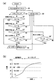
入力電圧Viをサンプリングする。尚、サンプリング周期ΔTは、ロードダンプ時の入力電圧Viの急変に追従できる程度に短い時間に設定する。
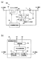
Q1,Q3 主スイッチ素子
Q2,Q4 整流スイッチ素子
Tr2,Tr4 整流トランジスタ素子
Di2,Di4 整流ダイオード素子
L インダクタ
C 平滑コンデンサ
50,50a 制御駆動回路部
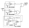
51 高Vi,高dVi/dt判定回路
Claims (14)
- ハイサイドの主スイッチ素子とローサイドの整流スイッチ素子を有してなる同期整流型のDC−DCコンバータであって、
前記整流スイッチ素子が、整流トランジスタ素子と該整流トランジスタ素子に逆並列に接続されてなる整流ダイオード素子とで構成されてなり、
前記主スイッチ素子と前記整流トランジスタ素子のオン・オフ状態を制御する制御駆動回路部を有してなり、
前記制御駆動回路部において、
前記主スイッチ素子への入力電圧を検知し、
前記入力電圧または前記入力電圧の上昇率を判定して、該判定値が所定の基準値を越えた時、前記主スイッチ素子と前記整流トランジスタ素子の相補的なオン・オフ動作を解除し、前記相補的なオン・オフ動作時のデッドタイムより長い時間、前記主スイッチ素子と前記整流トランジスタ素子が共にオフとなる状態が設定されてなることを特徴とするDC−DCコンバータ。 - 前記入力電圧および前記入力電圧の上昇率の両者を判定して、前記主スイッチ素子と前記整流トランジスタ素子の相補的なオン・オフ動作を解除することを特徴とする請求項1に記載のDC−DCコンバータ。
- 前記判定値が所定の基準値を越えた状態で、前記整流トランジスタ素子を常にオフ状態とすることを特徴とする請求項1または2に記載のDC−DCコンバータ。
- 前記判定値が所定の基準値を越えた状態で、前記整流トランジスタ素子のオン信号のパルス幅は前記解除前と同じで、前記整流トランジスタ素子のオン信号の繰り返し周期を前記解除前より遅くすることを特徴とする請求項1または2に記載のDC−DCコンバータ。
- 前記判定値が所定の基準値を越えた状態で、前記主スイッチ素子のオン信号のパルス幅は前記解除前と同じで、前記主スイッチ素子のオン信号の繰り返し周期を前記解除前より遅くすることを特徴とする請求項1乃至4のいずれか一項に記載のDC−DCコンバータ。
- 前記判定値が所定の基準値を越えた状態で、前記主スイッチ素子および前記整流トランジスタ素子のスイッチング速度を、前記解除前より低下させることを特徴とする請求項1乃至5のいずれか一項に記載のDC−DCコンバータ。
- 前記入力電圧または前記入力電圧の上昇率の判定が、デジタル回路のソフト演算によりなされることを特徴とする請求項1乃至6のいずれか一項に記載のDC−DCコンバータ。
- 前記入力電圧または前記入力電圧の上昇率の判定が、電子回路によりなされることを特徴とする請求項1乃至6のいずれか一項に記載のDC−DCコンバータ。
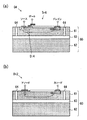
- 前記整流ダイオード素子が、ショットキバリア型ダイオードであることを特徴とする請求項1乃至8のいずれか一項に記載のDC−DCコンバータ。
- 前記整流トランジスタ素子が、MOSトランジスタ素子であり、
前記整流ダイオード素子が、前記MOSトランジスタ素子と同じ半導体基板に形成されてなるボディダイオード素子であることを特徴とする請求項1乃至8のいずれか一項に記載のDC−DCコンバータ。 - 前記DC−DCコンバータにおいて、
前記主スイッチ素子に流れる電流を検知することを特徴とする請求項10に記載のDC−DCコンバータ。 - 前記主スイッチ素子と前記整流スイッチ素子が、同じSOI基板に形成されてなることを特徴とする請求項1乃至11のいずれか一項に記載のDC−DCコンバータ。
- 前記DC−DCコンバータが、車載用であることを特徴とする請求項1乃至12のいずれか一項に記載のDC−DCコンバータ。
- 前記基準値が、ロードダンプサージに対して設定されてなることを特徴とする請求項13に記載のDC−DCコンバータ。
Priority Applications (2)
| Application Number | Priority Date | Filing Date | Title |
|---|---|---|---|
| JP2009198538A JP4666096B2 (ja) | 2008-09-04 | 2009-08-28 | Dc−dcコンバータ |
| US12/585,123 US8179106B2 (en) | 2008-09-04 | 2009-09-03 | DC-DC converter |
Applications Claiming Priority (2)
| Application Number | Priority Date | Filing Date | Title |
|---|---|---|---|
| JP2008227530 | 2008-09-04 | ||
| JP2009198538A JP4666096B2 (ja) | 2008-09-04 | 2009-08-28 | Dc−dcコンバータ |
Publications (2)
| Publication Number | Publication Date |
|---|---|
| JP2010088291A true JP2010088291A (ja) | 2010-04-15 |
| JP4666096B2 JP4666096B2 (ja) | 2011-04-06 |
Family
ID=41798676
Family Applications (1)
| Application Number | Title | Priority Date | Filing Date |
|---|---|---|---|
| JP2009198538A Expired - Fee Related JP4666096B2 (ja) | 2008-09-04 | 2009-08-28 | Dc−dcコンバータ |
Country Status (2)
| Country | Link |
|---|---|
| US (1) | US8179106B2 (ja) |
| JP (1) | JP4666096B2 (ja) |
Cited By (3)
| Publication number | Priority date | Publication date | Assignee | Title |
|---|---|---|---|---|
| WO2014006838A1 (ja) * | 2012-07-06 | 2014-01-09 | パナソニック株式会社 | スイッチング電源装置および半導体装置 |
| US9071143B2 (en) | 2013-02-21 | 2015-06-30 | Kabushiki Kaisha Toshiba | Semiconductor device |
| WO2020202967A1 (ja) * | 2019-04-02 | 2020-10-08 | 株式会社オートネットワーク技術研究所 | 車載用電圧変換装置 |
Families Citing this family (9)
| Publication number | Priority date | Publication date | Assignee | Title |
|---|---|---|---|---|
| JP4762824B2 (ja) * | 2006-08-10 | 2011-08-31 | 株式会社豊田中央研究所 | 電力変換回路 |
| CN101944845B (zh) * | 2010-08-06 | 2012-09-05 | 东南大学 | 死区时间自适应控制的开关级电路 |
| KR101788218B1 (ko) * | 2011-01-06 | 2017-10-20 | 삼성디스플레이 주식회사 | Dc-dc 컨버터 및 이를 이용한 이동통신 단말기 |
| CN102590620A (zh) * | 2011-01-12 | 2012-07-18 | 鸿富锦精密工业(深圳)有限公司 | 电阻测定电路 |
| TWI467185B (zh) * | 2011-01-17 | 2015-01-01 | Hon Hai Prec Ind Co Ltd | 電阻測定電路 |
| JP6069958B2 (ja) * | 2012-08-27 | 2017-02-01 | 富士電機株式会社 | スイッチング電源装置 |
| CN105471286B (zh) * | 2015-12-10 | 2017-09-29 | 无锡华润矽科微电子有限公司 | 同步整流电路、无线充电系统以及同步整流方法 |
| KR102583956B1 (ko) | 2018-05-10 | 2023-09-27 | 한국전자통신연구원 | 전력 컨버터 및 전력 컨버터의 데드-타임 제어 회로 |
| JP7455700B2 (ja) * | 2020-08-17 | 2024-03-26 | 矢崎総業株式会社 | スイッチング素子駆動装置 |
Citations (6)
| Publication number | Priority date | Publication date | Assignee | Title |
|---|---|---|---|---|
| JPH03218264A (ja) * | 1990-01-24 | 1991-09-25 | Mitsubishi Electric Corp | 整流装置 |
| JP2005073460A (ja) * | 2003-08-27 | 2005-03-17 | Tdk Corp | スイッチング電源装置 |
| JP2006149128A (ja) * | 2004-11-22 | 2006-06-08 | Funai Electric Co Ltd | スイッチング電源 |
| JP2006325287A (ja) * | 2005-05-17 | 2006-11-30 | Toyota Industries Corp | 過電圧保護機能付き電源装置および過電圧保護回路 |
| JP2007129853A (ja) * | 2005-11-04 | 2007-05-24 | Toyota Motor Corp | 電源装置 |
| JP2009124052A (ja) * | 2007-11-16 | 2009-06-04 | Denso Corp | Dc−dcコンバータ |
Family Cites Families (10)
| Publication number | Priority date | Publication date | Assignee | Title |
|---|---|---|---|---|
| US4801859A (en) * | 1986-12-23 | 1989-01-31 | Sundstrand Corporation | Boost/buck DC/DC converter |
| JP3000798B2 (ja) | 1992-09-28 | 2000-01-17 | 日本電気株式会社 | スイッチング電源回路 |
| JP3416219B2 (ja) | 1993-09-27 | 2003-06-16 | キヤノン株式会社 | 電源装置 |
| US6046896A (en) * | 1995-08-11 | 2000-04-04 | Fijitsu Limited | DC-to-DC converter capable of preventing overvoltage |
| JP3335587B2 (ja) * | 1998-12-25 | 2002-10-21 | 富士通株式会社 | Dc−dcコンバータ回路 |
| JP2001161068A (ja) | 1999-11-30 | 2001-06-12 | Matsushita Electric Ind Co Ltd | 供給電力制限機能付きdc−dcコンバータ |
| JP2002272093A (ja) | 2001-03-09 | 2002-09-20 | Cosel Co Ltd | アクティブ型力率改善回路 |
| JP2007151271A (ja) | 2005-11-25 | 2007-06-14 | Matsushita Electric Ind Co Ltd | Dc−dcコンバータ |
| JP4797631B2 (ja) | 2006-01-06 | 2011-10-19 | 富士電機株式会社 | Dc−dcコンバータ及びその制御方法 |
| JP2008141894A (ja) | 2006-12-04 | 2008-06-19 | Mitsubishi Electric Corp | 突入電流防止回路 |
-
2009
- 2009-08-28 JP JP2009198538A patent/JP4666096B2/ja not_active Expired - Fee Related
- 2009-09-03 US US12/585,123 patent/US8179106B2/en not_active Expired - Fee Related
Patent Citations (6)
| Publication number | Priority date | Publication date | Assignee | Title |
|---|---|---|---|---|
| JPH03218264A (ja) * | 1990-01-24 | 1991-09-25 | Mitsubishi Electric Corp | 整流装置 |
| JP2005073460A (ja) * | 2003-08-27 | 2005-03-17 | Tdk Corp | スイッチング電源装置 |
| JP2006149128A (ja) * | 2004-11-22 | 2006-06-08 | Funai Electric Co Ltd | スイッチング電源 |
| JP2006325287A (ja) * | 2005-05-17 | 2006-11-30 | Toyota Industries Corp | 過電圧保護機能付き電源装置および過電圧保護回路 |
| JP2007129853A (ja) * | 2005-11-04 | 2007-05-24 | Toyota Motor Corp | 電源装置 |
| JP2009124052A (ja) * | 2007-11-16 | 2009-06-04 | Denso Corp | Dc−dcコンバータ |
Cited By (6)
| Publication number | Priority date | Publication date | Assignee | Title |
|---|---|---|---|---|
| WO2014006838A1 (ja) * | 2012-07-06 | 2014-01-09 | パナソニック株式会社 | スイッチング電源装置および半導体装置 |
| JPWO2014006838A1 (ja) * | 2012-07-06 | 2016-06-02 | パナソニックIpマネジメント株式会社 | スイッチング電源装置および半導体装置 |
| US9425678B2 (en) | 2012-07-06 | 2016-08-23 | Panasonic Intellectual Property Management Co., Ltd. | Switching power supply apparatus and semiconductor device |
| US9071143B2 (en) | 2013-02-21 | 2015-06-30 | Kabushiki Kaisha Toshiba | Semiconductor device |
| US9531269B2 (en) | 2013-02-21 | 2016-12-27 | Kabushiki Kaisha Toshiba | Semiconductor device |
| WO2020202967A1 (ja) * | 2019-04-02 | 2020-10-08 | 株式会社オートネットワーク技術研究所 | 車載用電圧変換装置 |
Also Published As
| Publication number | Publication date |
|---|---|
| US8179106B2 (en) | 2012-05-15 |
| JP4666096B2 (ja) | 2011-04-06 |
| US20100060254A1 (en) | 2010-03-11 |
Similar Documents
| Publication | Publication Date | Title |
|---|---|---|
| JP4666096B2 (ja) | Dc−dcコンバータ | |
| US8193793B2 (en) | DC-DC converter | |
| TWI407673B (zh) | Switch control circuit | |
| JP4985003B2 (ja) | Dc−dcコンバータ | |
| JP4481879B2 (ja) | スイッチング電源装置 | |
| JP2000092824A (ja) | スイッチングレギュレータおよびlsiシステム | |
| JP5229495B2 (ja) | スイッチング装置及びその制御方法 | |
| CN108141131B (zh) | 多相转换器 | |
| JP5866920B2 (ja) | スイッチング装置及びその制御方法 | |
| JP2006060977A (ja) | 電源制御用半導体集積回路およびスイッチング電源装置 | |
| JP6818140B2 (ja) | 電力変換装置 | |
| JP2009268325A (ja) | フライバックコンバータ | |
| JP3425403B2 (ja) | 半導体装置、および、この半導体装置を用いたスイッチング電源装置 | |
| JP2009225642A (ja) | 電源装置および半導体集積回路装置 | |
| JP2008079448A (ja) | 昇圧電源装置 | |
| JP2009044814A (ja) | 同期整流型dc/dcコンバータ | |
| JP2010158112A (ja) | ゲート駆動回路 | |
| JP7676847B2 (ja) | スイッチング制御回路、共振型コンバータ | |
| JP6588634B2 (ja) | スイッチングレギュレータ、半導体集積回路、及び電子機器 | |
| JP2008035633A (ja) | インバータ装置 | |
| JP2008271758A (ja) | Dc−dcコンバータ | |
| JP2002051541A (ja) | スイッチング電源装置及びスイッチング電源用半導体装置 | |
| JP2007282443A (ja) | スイッチングレギュレータ | |
| JP5209273B2 (ja) | 電源装置及びこれを備えた電子機器 | |
| JP7018505B2 (ja) | Dc-dcコンバータ |
Legal Events
| Date | Code | Title | Description |
|---|---|---|---|
| A621 | Written request for application examination |
Free format text: JAPANESE INTERMEDIATE CODE: A621 Effective date: 20100215 |
|
| A977 | Report on retrieval |
Free format text: JAPANESE INTERMEDIATE CODE: A971007 Effective date: 20100720 |
|
| A131 | Notification of reasons for refusal |
Free format text: JAPANESE INTERMEDIATE CODE: A131 Effective date: 20100817 |
|
| A521 | Written amendment |
Free format text: JAPANESE INTERMEDIATE CODE: A523 Effective date: 20101013 |
|
| TRDD | Decision of grant or rejection written | ||
| A01 | Written decision to grant a patent or to grant a registration (utility model) |
Free format text: JAPANESE INTERMEDIATE CODE: A01 Effective date: 20101214 |
|
| A01 | Written decision to grant a patent or to grant a registration (utility model) |
Free format text: JAPANESE INTERMEDIATE CODE: A01 |
|
| A61 | First payment of annual fees (during grant procedure) |
Free format text: JAPANESE INTERMEDIATE CODE: A61 Effective date: 20101227 |
|
| FPAY | Renewal fee payment (event date is renewal date of database) |
Free format text: PAYMENT UNTIL: 20140121 Year of fee payment: 3 |
|
| R151 | Written notification of patent or utility model registration |
Ref document number: 4666096 Country of ref document: JP Free format text: JAPANESE INTERMEDIATE CODE: R151 |
|
| FPAY | Renewal fee payment (event date is renewal date of database) |
Free format text: PAYMENT UNTIL: 20140121 Year of fee payment: 3 |
|
| R250 | Receipt of annual fees |
Free format text: JAPANESE INTERMEDIATE CODE: R250 |
|
| R250 | Receipt of annual fees |
Free format text: JAPANESE INTERMEDIATE CODE: R250 |
|
| R250 | Receipt of annual fees |
Free format text: JAPANESE INTERMEDIATE CODE: R250 |
|
| R250 | Receipt of annual fees |
Free format text: JAPANESE INTERMEDIATE CODE: R250 |
|
| R250 | Receipt of annual fees |
Free format text: JAPANESE INTERMEDIATE CODE: R250 |
|
| R250 | Receipt of annual fees |
Free format text: JAPANESE INTERMEDIATE CODE: R250 |
|
| LAPS | Cancellation because of no payment of annual fees |