JP2010034118A - 基板処理装置 - Google Patents
基板処理装置 Download PDFInfo
- Publication number
- JP2010034118A JP2010034118A JP2008191882A JP2008191882A JP2010034118A JP 2010034118 A JP2010034118 A JP 2010034118A JP 2008191882 A JP2008191882 A JP 2008191882A JP 2008191882 A JP2008191882 A JP 2008191882A JP 2010034118 A JP2010034118 A JP 2010034118A
- Authority
- JP
- Japan
- Prior art keywords
- substrate
- polishing
- wafer
- unit
- image
- Prior art date
- Legal status (The legal status is an assumption and is not a legal conclusion. Google has not performed a legal analysis and makes no representation as to the accuracy of the status listed.)
- Granted
Links
- 239000000758 substrate Substances 0.000 title claims abstract description 178
- 238000012545 processing Methods 0.000 title claims abstract description 116
- 238000005498 polishing Methods 0.000 claims abstract description 289
- 238000003384 imaging method Methods 0.000 claims abstract description 165
- 230000002093 peripheral effect Effects 0.000 claims abstract description 105
- 238000007689 inspection Methods 0.000 claims abstract description 31
- 230000007246 mechanism Effects 0.000 claims description 78
- 238000000034 method Methods 0.000 claims description 39
- 238000005259 measurement Methods 0.000 claims description 37
- 238000003860 storage Methods 0.000 claims description 10
- 238000012805 post-processing Methods 0.000 claims description 7
- 235000012431 wafers Nutrition 0.000 description 256
- 238000004140 cleaning Methods 0.000 description 29
- 238000010586 diagram Methods 0.000 description 22
- XLYOFNOQVPJJNP-UHFFFAOYSA-N water Substances O XLYOFNOQVPJJNP-UHFFFAOYSA-N 0.000 description 21
- 230000003287 optical effect Effects 0.000 description 16
- 238000001514 detection method Methods 0.000 description 13
- 238000001035 drying Methods 0.000 description 13
- 210000000078 claw Anatomy 0.000 description 12
- 238000011084 recovery Methods 0.000 description 10
- 230000008569 process Effects 0.000 description 9
- 238000012546 transfer Methods 0.000 description 8
- 238000004891 communication Methods 0.000 description 6
- 230000004048 modification Effects 0.000 description 6
- 238000012986 modification Methods 0.000 description 6
- 230000003746 surface roughness Effects 0.000 description 6
- XUIMIQQOPSSXEZ-UHFFFAOYSA-N Silicon Chemical compound [Si] XUIMIQQOPSSXEZ-UHFFFAOYSA-N 0.000 description 5
- 239000007788 liquid Substances 0.000 description 5
- 238000007517 polishing process Methods 0.000 description 5
- 229910052710 silicon Inorganic materials 0.000 description 5
- 239000010703 silicon Substances 0.000 description 5
- 230000009471 action Effects 0.000 description 4
- 230000008859 change Effects 0.000 description 4
- 239000003086 colorant Substances 0.000 description 4
- 230000004069 differentiation Effects 0.000 description 4
- 238000000227 grinding Methods 0.000 description 4
- 238000005286 illumination Methods 0.000 description 4
- 239000006061 abrasive grain Substances 0.000 description 3
- 238000013459 approach Methods 0.000 description 3
- 239000011162 core material Substances 0.000 description 3
- 238000011065 in-situ storage Methods 0.000 description 3
- 230000001965 increasing effect Effects 0.000 description 3
- 239000000463 material Substances 0.000 description 3
- 239000004065 semiconductor Substances 0.000 description 3
- 230000007423 decrease Effects 0.000 description 2
- 239000010432 diamond Substances 0.000 description 2
- 230000006870 function Effects 0.000 description 2
- 238000003672 processing method Methods 0.000 description 2
- 239000002699 waste material Substances 0.000 description 2
- JOYRKODLDBILNP-UHFFFAOYSA-N Ethyl urethane Chemical compound CCOC(N)=O JOYRKODLDBILNP-UHFFFAOYSA-N 0.000 description 1
- 229910004298 SiO 2 Inorganic materials 0.000 description 1
- 238000001816 cooling Methods 0.000 description 1
- 229910003460 diamond Inorganic materials 0.000 description 1
- 238000009826 distribution Methods 0.000 description 1
- 230000000694 effects Effects 0.000 description 1
- 230000003028 elevating effect Effects 0.000 description 1
- 238000005530 etching Methods 0.000 description 1
- 239000004744 fabric Substances 0.000 description 1
- 238000004519 manufacturing process Methods 0.000 description 1
- 229910021645 metal ion Inorganic materials 0.000 description 1
- 230000000116 mitigating effect Effects 0.000 description 1
- 239000013307 optical fiber Substances 0.000 description 1
- 239000013618 particulate matter Substances 0.000 description 1
- 238000003825 pressing Methods 0.000 description 1
- 239000011347 resin Substances 0.000 description 1
- 229920005989 resin Polymers 0.000 description 1
- 230000004044 response Effects 0.000 description 1
- 239000000126 substance Substances 0.000 description 1
- 239000008400 supply water Substances 0.000 description 1
- 238000012360 testing method Methods 0.000 description 1
- 229910021642 ultra pure water Inorganic materials 0.000 description 1
- 239000012498 ultrapure water Substances 0.000 description 1
Images


Classifications
-
- B—PERFORMING OPERATIONS; TRANSPORTING
- B24—GRINDING; POLISHING
- B24B—MACHINES, DEVICES, OR PROCESSES FOR GRINDING OR POLISHING; DRESSING OR CONDITIONING OF ABRADING SURFACES; FEEDING OF GRINDING, POLISHING, OR LAPPING AGENTS
- B24B9/00—Machines or devices designed for grinding edges or bevels on work or for removing burrs; Accessories therefor
- B24B9/02—Machines or devices designed for grinding edges or bevels on work or for removing burrs; Accessories therefor characterised by a special design with respect to properties of materials specific to articles to be ground
- B24B9/06—Machines or devices designed for grinding edges or bevels on work or for removing burrs; Accessories therefor characterised by a special design with respect to properties of materials specific to articles to be ground of non-metallic inorganic material, e.g. stone, ceramics, porcelain
- B24B9/065—Machines or devices designed for grinding edges or bevels on work or for removing burrs; Accessories therefor characterised by a special design with respect to properties of materials specific to articles to be ground of non-metallic inorganic material, e.g. stone, ceramics, porcelain of thin, brittle parts, e.g. semiconductors, wafers
-
- B—PERFORMING OPERATIONS; TRANSPORTING
- B24—GRINDING; POLISHING
- B24B—MACHINES, DEVICES, OR PROCESSES FOR GRINDING OR POLISHING; DRESSING OR CONDITIONING OF ABRADING SURFACES; FEEDING OF GRINDING, POLISHING, OR LAPPING AGENTS
- B24B21/00—Machines or devices using grinding or polishing belts; Accessories therefor
- B24B21/004—Machines or devices using grinding or polishing belts; Accessories therefor using abrasive rolled strips
-
- B—PERFORMING OPERATIONS; TRANSPORTING
- B24—GRINDING; POLISHING
- B24B—MACHINES, DEVICES, OR PROCESSES FOR GRINDING OR POLISHING; DRESSING OR CONDITIONING OF ABRADING SURFACES; FEEDING OF GRINDING, POLISHING, OR LAPPING AGENTS
- B24B37/00—Lapping machines or devices; Accessories
- B24B37/005—Control means for lapping machines or devices
- B24B37/013—Devices or means for detecting lapping completion
-
- B—PERFORMING OPERATIONS; TRANSPORTING
- B24—GRINDING; POLISHING
- B24B—MACHINES, DEVICES, OR PROCESSES FOR GRINDING OR POLISHING; DRESSING OR CONDITIONING OF ABRADING SURFACES; FEEDING OF GRINDING, POLISHING, OR LAPPING AGENTS
- B24B49/00—Measuring or gauging equipment for controlling the feed movement of the grinding tool or work; Arrangements of indicating or measuring equipment, e.g. for indicating the start of the grinding operation
- B24B49/12—Measuring or gauging equipment for controlling the feed movement of the grinding tool or work; Arrangements of indicating or measuring equipment, e.g. for indicating the start of the grinding operation involving optical means
Landscapes
- Engineering & Computer Science (AREA)
- Mechanical Engineering (AREA)
- Chemical & Material Sciences (AREA)
- Ceramic Engineering (AREA)
- Inorganic Chemistry (AREA)
- Mechanical Treatment Of Semiconductor (AREA)
- Constituent Portions Of Griding Lathes, Driving, Sensing And Control (AREA)
- Testing Or Measuring Of Semiconductors Or The Like (AREA)
Abstract
【解決手段】本発明の基板処理装は、置基板Wの周縁部を研磨する研磨ユニット70A,70Bと、研磨ユニット70A,70Bにより研磨された基板Wの周縁部を撮像する撮像モジュール131と、撮像モジュール131により撮像された画像から基板の研磨状態を検査する画像処理部132とを備え、撮像モジュール131は、研磨ユニット研磨ユニット70A,70Bが基板Wの周縁部を研磨していないときに基板の周縁部を撮像する。
【選択図】図9
Description
本発明の好ましい態様は、前記撮像モジュールは、基板の周縁部を多方向から撮像することを特徴とする。
本発明の好ましい態様は、前記撮像モジュールは、基板の周縁部に近接して配置されたプリズムと、前記プリズムを通じて基板の周縁部を撮像する撮像カメラとを備えていることを特徴とする。
本発明の好ましい態様は、前記撮像モジュールは、複数の撮像カメラを有していることを特徴とする。
本発明の好ましい態様は、前記画像処理部は、前記撮像モジュールにより取得された画像の色を数値に表し、前記数値が予め設定された閾値を上回ったとき、または下回ったときに、除去すべき対象物が前記周縁部から除去されたと判断することを特徴とする。
本発明の好ましい態様は、前記撮像モジュールは、基板の周縁部の静止画像を取得することを特徴とする。
本発明の好ましい態様は、前記撮像モジュールは、基板の周縁部の積算画像を取得することを特徴とする。
本発明の好ましい態様は、前記撮像モジュールは、ラインスキャンカメラを有していることを特徴とする。
本発明の好ましい態様は、前記撮像モジュールは、視野の異なる複数のカメラを有していることを特徴とする。
本発明の好ましい態様は、前記測定ユニットは、基板をその中心軸回りに回転させる基板保持回転機構を有しており、前記撮像モジュールは、前記基板保持回転機構によって保持された基板の周縁部に近接して配置されていることを特徴とする。
本発明の好ましい態様は、前記少なくとも1つの後処理ユニットは、基板をその中心軸回りに回転させる基板保持回転機構を有しており、前記撮像モジュールは、前記基板保持回転機構によって保持された基板の周縁部に近接して配置されていることを特徴とする。
本発明の好ましい態様は、前記基板処理装置は、前記撮像モジュールによって取得された画像を保存する記憶装置と、前記記憶装置に保存された画像を表示する画像表示部とをさらに備えることを特徴とする。
本発明の好ましい態様は、前記記憶装置は、前記画像が取得された位置を示す情報を該画像と共に保存し、前記画像表示部は、要求された位置の画像を表示するように構成されることを特徴とする。
図1(a)および図1(b)は、半導体ウエハ等の基板(以下「ウエハ」と称す。)の周縁部を示す部分拡大断面図である。より詳しくは、図1(a)は、周縁部の断面が複数の直線部で構成されたいわゆるストレート型のウエハWの断面図であり、図1(b)は、周縁部の断面が曲線部で構成されたいわゆるラウンド型のウエハWの断面図である。
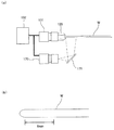
この測定ユニット30は、ウエハWの外径寸法(直径)を計測する直径計測機構を備えたもので、計測したウエハの直径からウエハ側面の研磨量を計測するものである。この測定ユニット30は、基板保持回転機構61と、該基板保持回転機構61で保持されたウエハWの周縁部の所定位置の上下に設置した一対の投光装置32及び受光装置33からなるセンサ機構(レーザーセンサ)31を具備している。投光装置32はレーザー光を投光する装置である。
図11はステップ・アンド・リピート方式でのウエハの撮像位置の例を示す図であり、図12はステップ・アンド・リピート方式の動作シーケンスを示すフローチャートである。
図11に示すように、この方式では、ウエハWの周縁部上での複数の撮像位置が予め設定されている。
この方式では、ウエハWの周縁部がその全周に亘って撮像される。画像処理部132はステップモータ150に指令信号を送り、ウエハWを回転させる(ステップ1)。ウエハWの回転位置はロータリーエンコーダ151により計測される(ステップ2)。
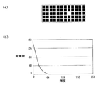
上述したように、画像処理部132は、ターゲット領域の色の変化に基づいて膜除去を判断する。画像処理部132には、予めターゲット色が登録されており、画像処理部132は、ターゲット領域の色が、登録されている所定のターゲット色に一致するときには、ウエハWから膜が除去されたと判定する。より詳しくは、画像処理部132は、ターゲット領域におけるターゲット色の画素の数が増加して所定の閾値を上回ったとき、またはターゲット領域におけるターゲット色の画素の数が減少して所定の閾値を下回ったとき、ウエハWから膜が除去されたと判定する。
まず、画像処理部132にターゲット色としてシリコンの色(通常は白)を登録する(ステップ1)。上述したように、色の選択は1つに限らず、複数の色を選択することができる。次に、ターゲット領域を指定する(ステップ2)。そして、ターゲット領域内におけるターゲット色の画素の数Nが所定の閾値Pを上回っている場合は、画像処理部132は研磨によって膜が除去されたと判断する。これは、研磨によって膜が除去されると、下地層のシリコンの色が表出するからである。一方、ターゲット領域内におけるターゲット色の画素の数Nが所定の閾値P以下である場合は、画像処理部132は膜がウエハW上に残存していると判断する(ステップ3)。
図19に示すように、まず、画像処理部132にターゲット色として除去対象膜の色を登録する(ステップ1)。この場合も、色の選択は1つに限らず、複数の色を選択することもできる。次に、ターゲット領域を指定する(ステップ2)。そして、ターゲット領域内におけるターゲット色の画素の数Nが所定の閾値Pを下回っている場合は、画像処理部132は研磨によって膜が除去されたと判断する。これは、研磨によって膜が除去されると、膜の色が消えるからである。一方、ターゲット領域内におけるターゲット色の画素の数Nが所定の閾値P以上である場合は、画像処理部132は膜がウエハW上に残存していると判断する(ステップ3)。
表面粗さを検出するためには、ウエハの静止画像を取得することが好ましい。したがって、表面粗さ検出方法では、上述したステップ・アンド・リピート方式を用いるか、またはスキャン方式とインラインスキャンカメラとの組み合わせを用いることが好ましい。
2 クリーンルーム
3a ハウジング
3 側壁
10 ロードアンロードポート
11A,11B ウエハ供給回収装置
12A,12B ウエハカセット
20A 第1搬送ロボット
20B 第2搬送ロボット
30 測定ユニット
31 センサ機構
32 投光装置
33 受光装置
34 レーザー光
61 基板保持回転機構
62 上段チャック
62a 爪部
63 下段チャック
63a 爪部
64 回転軸
70A 第1研磨ユニット
70B 第2研磨ユニット
71 筐体
72 基板保持回転部
73 基板保持テーブル
73a 溝部
73b 連通路
74 支持軸
74a 連通路
75 回転駆動装置
76 真空ライン
77 圧縮空気供給ライン
78 吸着パッド
80 基板受渡機構
81 アーム
82 コマ
83 ベベル研磨部
84 研磨テープ
84a 研磨面
85 ベベル研磨ヘッド
86,86 送りローラ
87 基部
88 研磨テープ送り機構
88a 供給リール
88b 回収リール
89 芯材
90 ノッチ研磨部
91 研磨テープ
91a 研磨面
92 ノッチ研磨ヘッド
93,93 送りローラ
94 研磨テープ送り機構
94a 供給リール
94b 回収リール
95,96 研磨水供給ノズル
97 研磨水供給ノズル
100 1次洗浄ユニット
110 2次洗浄・乾燥ユニット
131 撮像モジュール
132 画像処理部
135 プリズム
136 撮像カメラ
137 フォーカスレンズユニット
140 レンズ
141 アクチュエータ
142 ハーフミラー
144 光源
145 レンズ
150 ステップモータ
151 ロータリーエンコーダ
160A〜160C 末端撮像部
163A〜163D 照明部
165 支持部材
171 ミラー
Claims (19)
- 基板の周縁部を研磨する研磨ユニットと、
前記研磨ユニットにより研磨された基板の周縁部を撮像する撮像モジュールと、
前記撮像モジュールにより撮像された画像から基板の研磨状態を検査する画像処理部とを備え、
前記撮像モジュールは、前記研磨ユニットが基板の周縁部を研磨していないときに前記基板の周縁部を撮像することを特徴とする基板処理装置。 - 前記基板処理装置は、前記研磨ユニットの研磨条件を決定する研磨条件決定部をさらに備え、
前記画像処理部の検査結果は前記研磨条件決定部に送られ、
前記研磨条件決定部は前記検査結果に基づいて前記研磨ユニットでの研磨条件を決定することを特徴とする請求項1に記載の基板処理装置。 - 前記撮像モジュールは、基板の周縁部を多方向から撮像することを特徴とする請求項1に記載の基板処理装置。
- 前記撮像モジュールは、基板の周縁部に近接して配置されたプリズムと、前記プリズムを通じて基板の周縁部を撮像する撮像カメラとを備えていることを特徴とする請求項3に記載の基板処理装置。
- 前記撮像モジュールは、複数の撮像カメラを有していることを特徴とする請求項3に記載の基板処理装置。
- 前記画像処理部は、前記撮像モジュールによって取得された画像の色に基づいて基板の周縁部の研磨状態を検査することを特徴とする請求項1に記載の基板処理装置。
- 前記画像処理部は、
前記撮像モジュールにより取得された画像の色を数値に表し、
前記数値が予め設定された閾値を上回ったとき、または下回ったときに、除去すべき対象物が前記周縁部から除去されたと判断することを特徴とする請求項6に記載の基板処理装置。 - 前記基板処理装置は、基板をその中心軸回りに回転させる基板保持回転機構をさらに備え、
前記撮像モジュールは、前記基板回転機構によって保持された基板の周縁部に近接して配置されており、
前記基板保持回転機構によって基板を断続的または連続的に回転させながら、前記撮像モジュールは基板の周縁部を撮像することを特徴とする請求項1に記載の基板処理装置。 - 前記撮像モジュールは、基板の周縁部の静止画像を取得することを特徴とする請求項8に記載の基板処理装置。
- 前記撮像モジュールは、基板の周縁部の積算画像を取得することを特徴とする請求項8に記載の基板処理装置。
- 前記撮像モジュールは、ラインスキャンカメラを有していることを特徴とする請求項8に記載の基板処理装置。
- 前記撮像モジュールは、視野の異なる複数のカメラを有していることを特徴とする請求項1に記載の基板処理装置。
- 前記基板処理装置は、前記研磨ユニットによって研磨された基板の所定の物理量を測定する測定ユニットをさらに備えており、
前記撮像モジュールは、前記測定ユニットに組み込まれていることを特徴とする請求項1に記載の基板処理装置。 - 前記測定ユニットは、基板をその中心軸回りに回転させる基板保持回転機構を有しており、
前記撮像モジュールは、前記基板保持回転機構によって保持された基板の周縁部に近接して配置されていることを特徴とする請求項13に記載の基板処理装置。 - 前記基板処理装置は、前記研磨ユニットによって研磨された基板を後処理する少なくとも1つの後処理ユニットをさらに備えており、
前記撮像モジュールは、前記少なくとも1つの後処理ユニットに組み込まれていることを特徴とする請求項1に記載の基板処理装置。 - 前記少なくとも1つの後処理ユニットは、基板をその中心軸回りに回転させる基板保持回転機構を有しており、
前記撮像モジュールは、前記基板保持回転機構によって保持された基板の周縁部に近接して配置されていることを特徴とする請求項15に記載の基板処理装置。 - 前記基板処理装置は、前記画像処理部の検査結果を保存する記憶装置をさらに備えることを特徴とする請求項1に記載の基板処理装置。
- 前記基板処理装置は、
前記撮像モジュールによって取得された画像を保存する記憶装置と、
前記記憶装置に保存された画像を表示する画像表示部とをさらに備えることを特徴とする請求項1に記載の基板処理装置。 - 前記記憶装置は、前記画像が取得された位置を示す情報を該画像と共に保存し、
前記画像表示部は、要求された位置の画像を表示するように構成されることを特徴とする請求項18に記載の基板処理装置。
Priority Applications (2)
| Application Number | Priority Date | Filing Date | Title |
|---|---|---|---|
| JP2008191882A JP5160993B2 (ja) | 2008-07-25 | 2008-07-25 | 基板処理装置 |
| US12/458,814 US8414355B2 (en) | 2008-07-25 | 2009-07-23 | Substrate processing apparatus |
Applications Claiming Priority (1)
| Application Number | Priority Date | Filing Date | Title |
|---|---|---|---|
| JP2008191882A JP5160993B2 (ja) | 2008-07-25 | 2008-07-25 | 基板処理装置 |
Publications (3)
| Publication Number | Publication Date |
|---|---|
| JP2010034118A true JP2010034118A (ja) | 2010-02-12 |
| JP2010034118A5 JP2010034118A5 (ja) | 2010-12-16 |
| JP5160993B2 JP5160993B2 (ja) | 2013-03-13 |
Family
ID=41569066
Family Applications (1)
| Application Number | Title | Priority Date | Filing Date |
|---|---|---|---|
| JP2008191882A Active JP5160993B2 (ja) | 2008-07-25 | 2008-07-25 | 基板処理装置 |
Country Status (2)
| Country | Link |
|---|---|
| US (1) | US8414355B2 (ja) |
| JP (1) | JP5160993B2 (ja) |
Cited By (6)
| Publication number | Priority date | Publication date | Assignee | Title |
|---|---|---|---|---|
| KR101868786B1 (ko) * | 2017-08-08 | 2018-06-19 | 김인수 | 휴대기기 글라스 성형용 금형의 제조장치 |
| JP2019062011A (ja) * | 2017-09-25 | 2019-04-18 | 東京エレクトロン株式会社 | 基板処理装置 |
| JP2021015873A (ja) * | 2019-07-11 | 2021-02-12 | 株式会社荏原製作所 | 研磨装置および研磨方法 |
| JP2021133497A (ja) * | 2020-02-26 | 2021-09-13 | 上海東競自動化系統有限公司 | 表面傷を修復する方法及び装置 |
| WO2024224992A1 (ja) * | 2023-04-28 | 2024-10-31 | 株式会社Screenホールディングス | 撮像装置、基板観察装置、基板処理装置および撮像方法 |
| TWI898454B (zh) * | 2024-02-29 | 2025-09-21 | 東台精機股份有限公司 | 晶圓研磨裝置及晶圓研磨方法 |
Families Citing this family (16)
| Publication number | Priority date | Publication date | Assignee | Title |
|---|---|---|---|---|
| JP5254575B2 (ja) * | 2007-07-11 | 2013-08-07 | 株式会社東芝 | 研磨装置および研磨方法 |
| KR101236472B1 (ko) * | 2007-10-15 | 2013-02-22 | 삼성전자주식회사 | 웨이퍼 베벨 영역 폴리싱 장치 및 그 장치에서의 연마종말점 검출 방법 |
| JP5393039B2 (ja) | 2008-03-06 | 2014-01-22 | 株式会社荏原製作所 | 研磨装置 |
| US20100105290A1 (en) * | 2008-10-24 | 2010-04-29 | Applied Materials, Inc. | Methods and apparatus for indicating a polishing tape end |
| FR2975940A1 (fr) * | 2011-05-31 | 2012-12-07 | Forest Line Capdenac | Procede de controle du jeu entre bandes deposees par une tete de drapage et sous-ensemble de tete de drapage a dispositif de controle embarque. |
| JP5976331B2 (ja) * | 2012-02-03 | 2016-08-23 | 株式会社ディスコ | 研削装置 |
| JP6140439B2 (ja) * | 2012-12-27 | 2017-05-31 | 株式会社荏原製作所 | 研磨装置、及び研磨方法 |
| JP6100002B2 (ja) * | 2013-02-01 | 2017-03-22 | 株式会社荏原製作所 | 基板裏面の研磨方法および基板処理装置 |
| JP6071611B2 (ja) * | 2013-02-13 | 2017-02-01 | Mipox株式会社 | オリエンテーションフラット等切り欠き部を有する、結晶材料から成るウエハの周縁を、研磨テープを使用して研磨することにより円形ウエハを製造する方法 |
| JP2014200888A (ja) * | 2013-04-05 | 2014-10-27 | ローム株式会社 | 吸引保持装置およびウエハ研磨装置 |
| JP6327329B1 (ja) * | 2016-12-20 | 2018-05-23 | 株式会社Sumco | シリコンウェーハの研磨方法およびシリコンウェーハの製造方法 |
| JP6920849B2 (ja) * | 2017-03-27 | 2021-08-18 | 株式会社荏原製作所 | 基板処理方法および装置 |
| JP6713015B2 (ja) * | 2018-04-13 | 2020-06-24 | 株式会社大気社 | 自動研磨システム |
| CN109604116B (zh) * | 2018-11-29 | 2021-04-09 | 安徽荣泽科技有限公司 | 一种全自动特种胶带涂布机 |
| JP7282461B2 (ja) * | 2019-04-16 | 2023-05-29 | 株式会社ディスコ | 検査装置、及び加工装置 |
| JP2025083039A (ja) * | 2023-11-20 | 2025-05-30 | 株式会社荏原製作所 | 基板処理装置および基板処理方法 |
Citations (8)
| Publication number | Priority date | Publication date | Assignee | Title |
|---|---|---|---|---|
| JP2000114329A (ja) * | 1998-09-29 | 2000-04-21 | Yuhi Denshi Kk | 基板端部の研削面の検査方法とその装置 |
| JP2002208572A (ja) * | 2001-01-09 | 2002-07-26 | Ebara Corp | 研磨装置 |
| JP2005191179A (ja) * | 2003-12-25 | 2005-07-14 | Trecenti Technologies Inc | 半導体装置の製造方法および研磨装置 |
| JP2005217139A (ja) * | 2004-01-29 | 2005-08-11 | Dainippon Screen Mfg Co Ltd | 画像取得装置および画像取得方法 |
| JP2006220540A (ja) * | 2005-02-10 | 2006-08-24 | Central Glass Co Ltd | ガラス板の端面の欠陥検出装置および検出方法 |
| WO2006112530A1 (en) * | 2005-04-19 | 2006-10-26 | Ebara Corporation | Substrate processing apparatus |
| JP2007155448A (ja) * | 2005-12-02 | 2007-06-21 | Olympus Corp | 端面検査装置 |
| JP2009111079A (ja) * | 2007-10-29 | 2009-05-21 | Toshiba Corp | 基板の周縁部の処理方法および装置 |
Family Cites Families (23)
| Publication number | Priority date | Publication date | Assignee | Title |
|---|---|---|---|---|
| US4319270A (en) * | 1979-01-12 | 1982-03-09 | Kobe Steel, Ltd. | Surface inspection system for hot radiant material |
| IT1262263B (it) * | 1993-12-30 | 1996-06-19 | Delle Vedove Levigatrici Spa | Procedimento di levigatura per profili curvi e sagomati e macchina levigatrice che realizza tale procedimento |
| JPH07276229A (ja) | 1994-04-01 | 1995-10-24 | Nippon Steel Corp | 半導体ウエハエッジ部研磨装置 |
| JPH08243891A (ja) * | 1995-03-07 | 1996-09-24 | Kao Corp | 基板のチャンファ加工装置 |
| US5604583A (en) * | 1995-03-20 | 1997-02-18 | Bausch & Lomb Incorporated | Computer vision inspection station |
| JP3580600B2 (ja) * | 1995-06-09 | 2004-10-27 | 株式会社ルネサステクノロジ | 半導体装置の製造方法およびそれに使用される半導体ウエハ並びにその製造方法 |
| JP2999712B2 (ja) | 1996-03-29 | 2000-01-17 | 住友金属工業株式会社 | 端部欠陥検査方法とその装置 |
| JP2000512564A (ja) * | 1996-06-15 | 2000-09-26 | ウノバ・ユー・ケイ・リミテッド | プラットホームに柔軟に取付けられた研削マシンスピンドル |
| DE19727226A1 (de) * | 1997-04-10 | 1998-10-22 | Fraunhofer Ges Forschung | Meßanordnung und Verfahren zum berührungslosen Erfassen der 3-dimensionalen Raumform einer Brillenfassungsnut |
| DE19804542C5 (de) * | 1998-02-05 | 2009-04-30 | Wernicke & Co Gmbh | Verfahren und Vorrichtung zum Bearbeiten von Brillengläsern |
| JP3425590B2 (ja) | 1998-06-04 | 2003-07-14 | 三菱住友シリコン株式会社 | 端部傷検査方法およびその装置 |
| CA2243090A1 (en) * | 1998-07-10 | 2000-01-10 | Timothy M. Richardson | Inverted darkfield contrast microscope and method |
| GB2351684B (en) * | 1999-07-03 | 2001-07-11 | Unova Uk Ltd | Improvement in and relating to edge grinding |
| DE10119662C2 (de) * | 2001-04-20 | 2003-04-10 | Loh Optikmaschinen Ag | Verfahren zur Randbearbeitung von optischen Linsen |
| JP3949941B2 (ja) | 2001-11-26 | 2007-07-25 | 株式会社東芝 | 半導体装置の製造方法および研磨装置 |
| JP2003209075A (ja) | 2002-01-15 | 2003-07-25 | Speedfam Co Ltd | ウェハエッジ研磨システム及びウェハエッジ研磨制御方法 |
| JP3629244B2 (ja) | 2002-02-19 | 2005-03-16 | 本多エレクトロン株式会社 | ウエーハ用検査装置 |
| KR100798322B1 (ko) * | 2002-03-21 | 2008-01-28 | 엘지.필립스 엘시디 주식회사 | 액정 패널의 연마량 보정 장치 및 방법 |
| FR2838364B1 (fr) * | 2002-04-12 | 2005-01-07 | Essilor Int | Procede de chanfreinage d'une lentille ophtalmique comporatnt une etape de releve sans contact |
| KR100832297B1 (ko) * | 2002-12-17 | 2008-05-26 | 엘지디스플레이 주식회사 | 액정 표시패널의 연마량 측정장치 및 측정방법 |
| JP4125148B2 (ja) | 2003-02-03 | 2008-07-30 | 株式会社荏原製作所 | 基板処理装置 |
| CN100429752C (zh) | 2004-02-25 | 2008-10-29 | 株式会社荏原制作所 | 抛光装置和衬底处理装置 |
| TWI352645B (en) | 2004-05-28 | 2011-11-21 | Ebara Corp | Apparatus for inspecting and polishing substrate r |
-
2008
- 2008-07-25 JP JP2008191882A patent/JP5160993B2/ja active Active
-
2009
- 2009-07-23 US US12/458,814 patent/US8414355B2/en active Active
Patent Citations (9)
| Publication number | Priority date | Publication date | Assignee | Title |
|---|---|---|---|---|
| JP2000114329A (ja) * | 1998-09-29 | 2000-04-21 | Yuhi Denshi Kk | 基板端部の研削面の検査方法とその装置 |
| JP2002208572A (ja) * | 2001-01-09 | 2002-07-26 | Ebara Corp | 研磨装置 |
| JP2005191179A (ja) * | 2003-12-25 | 2005-07-14 | Trecenti Technologies Inc | 半導体装置の製造方法および研磨装置 |
| JP2005217139A (ja) * | 2004-01-29 | 2005-08-11 | Dainippon Screen Mfg Co Ltd | 画像取得装置および画像取得方法 |
| JP2006220540A (ja) * | 2005-02-10 | 2006-08-24 | Central Glass Co Ltd | ガラス板の端面の欠陥検出装置および検出方法 |
| WO2006112530A1 (en) * | 2005-04-19 | 2006-10-26 | Ebara Corporation | Substrate processing apparatus |
| JP2008537316A (ja) * | 2005-04-19 | 2008-09-11 | 株式会社荏原製作所 | 基板処理装置 |
| JP2007155448A (ja) * | 2005-12-02 | 2007-06-21 | Olympus Corp | 端面検査装置 |
| JP2009111079A (ja) * | 2007-10-29 | 2009-05-21 | Toshiba Corp | 基板の周縁部の処理方法および装置 |
Cited By (10)
| Publication number | Priority date | Publication date | Assignee | Title |
|---|---|---|---|---|
| KR101868786B1 (ko) * | 2017-08-08 | 2018-06-19 | 김인수 | 휴대기기 글라스 성형용 금형의 제조장치 |
| WO2019031765A1 (ko) * | 2017-08-08 | 2019-02-14 | 김인수 | 휴대기기 글라스 성형용 금형의 제조장치 |
| JP2019062011A (ja) * | 2017-09-25 | 2019-04-18 | 東京エレクトロン株式会社 | 基板処理装置 |
| JP7029914B2 (ja) | 2017-09-25 | 2022-03-04 | 東京エレクトロン株式会社 | 基板処理装置 |
| JP2021015873A (ja) * | 2019-07-11 | 2021-02-12 | 株式会社荏原製作所 | 研磨装置および研磨方法 |
| JP7350544B2 (ja) | 2019-07-11 | 2023-09-26 | 株式会社荏原製作所 | 研磨装置および研磨方法 |
| JP2021133497A (ja) * | 2020-02-26 | 2021-09-13 | 上海東競自動化系統有限公司 | 表面傷を修復する方法及び装置 |
| JP7248991B2 (ja) | 2020-02-26 | 2023-03-30 | 上海東競自動化系統有限公司 | 表面傷を修復する方法及び装置 |
| WO2024224992A1 (ja) * | 2023-04-28 | 2024-10-31 | 株式会社Screenホールディングス | 撮像装置、基板観察装置、基板処理装置および撮像方法 |
| TWI898454B (zh) * | 2024-02-29 | 2025-09-21 | 東台精機股份有限公司 | 晶圓研磨裝置及晶圓研磨方法 |
Also Published As
| Publication number | Publication date |
|---|---|
| US20100022166A1 (en) | 2010-01-28 |
| JP5160993B2 (ja) | 2013-03-13 |
| US8414355B2 (en) | 2013-04-09 |
Similar Documents
| Publication | Publication Date | Title |
|---|---|---|
| JP5160993B2 (ja) | 基板処理装置 | |
| JP4916890B2 (ja) | 基板処理装置及び基板処理方法 | |
| US7682225B2 (en) | Polishing apparatus and substrate processing apparatus | |
| JP4125148B2 (ja) | 基板処理装置 | |
| KR101214507B1 (ko) | 기판 처리 장치, 기판 폴리싱 방법 및 기판 처리 방법 | |
| US20130044316A1 (en) | Device and method for inspecting moving semicondutor wafers | |
| TW200303807A (en) | Polishing apparatus and method for detecting foreign matter on polishing surface | |
| US20150017745A1 (en) | Polishing method and polishing apparatus | |
| KR101236472B1 (ko) | 웨이퍼 베벨 영역 폴리싱 장치 및 그 장치에서의 연마종말점 검출 방법 | |
| JP2001519021A (ja) | 光学検査モジュール、及び統合プロセス工具内で基板上の粒子及び欠陥を検出するための方法 | |
| JP2007331106A (ja) | 測定ステーション、研磨機械、ウェハを研磨するための方法、および、ウェハの光学的測定方法 | |
| JP4660494B2 (ja) | 研磨カートリッジ | |
| US8771038B2 (en) | Polishing apparatus | |
| TWI691715B (zh) | 檢測矽晶圓缺陷的自動光學檢測機構及方法 | |
| KR102873657B1 (ko) | 기판 세정 시스템에서 두께를 모니터링하기 위한 이미징 | |
| JP2008091951A (ja) | 基板処理装置 | |
| KR20070002257A (ko) | 웨이퍼 후면 결함 검출 장치 | |
| JP2020136498A (ja) | ウェハ加工異常検出装置と方法及び平面加工システム | |
| JP2024155058A (ja) | 膜厚測定装置、膜厚測定方法及び基板研磨装置 | |
| US7155963B2 (en) | Cleaning evaluation method for a substrate | |
| JP2005259967A (ja) | 化学機械研磨装置及び化学機械研磨方法 | |
| JP2006035353A (ja) | Cmp装置、cmp研磨方法、及び、半導体装置の製造方法 |
Legal Events
| Date | Code | Title | Description |
|---|---|---|---|
| A521 | Request for written amendment filed |
Free format text: JAPANESE INTERMEDIATE CODE: A523 Effective date: 20101101 |
|
| A621 | Written request for application examination |
Free format text: JAPANESE INTERMEDIATE CODE: A621 Effective date: 20101101 |
|
| A131 | Notification of reasons for refusal |
Free format text: JAPANESE INTERMEDIATE CODE: A131 Effective date: 20120911 |
|
| A977 | Report on retrieval |
Free format text: JAPANESE INTERMEDIATE CODE: A971007 Effective date: 20120912 |
|
| A521 | Request for written amendment filed |
Free format text: JAPANESE INTERMEDIATE CODE: A523 Effective date: 20121109 |
|
| TRDD | Decision of grant or rejection written | ||
| A01 | Written decision to grant a patent or to grant a registration (utility model) |
Free format text: JAPANESE INTERMEDIATE CODE: A01 Effective date: 20121204 |
|
| A61 | First payment of annual fees (during grant procedure) |
Free format text: JAPANESE INTERMEDIATE CODE: A61 Effective date: 20121213 |
|
| R150 | Certificate of patent or registration of utility model |
Ref document number: 5160993 Country of ref document: JP Free format text: JAPANESE INTERMEDIATE CODE: R150 Free format text: JAPANESE INTERMEDIATE CODE: R150 |
|
| FPAY | Renewal fee payment (event date is renewal date of database) |
Free format text: PAYMENT UNTIL: 20151221 Year of fee payment: 3 |
|
| R250 | Receipt of annual fees |
Free format text: JAPANESE INTERMEDIATE CODE: R250 |
|
| R250 | Receipt of annual fees |
Free format text: JAPANESE INTERMEDIATE CODE: R250 |
|
| R250 | Receipt of annual fees |
Free format text: JAPANESE INTERMEDIATE CODE: R250 |
|
| R250 | Receipt of annual fees |
Free format text: JAPANESE INTERMEDIATE CODE: R250 |
|
| R250 | Receipt of annual fees |
Free format text: JAPANESE INTERMEDIATE CODE: R250 |
|
| R250 | Receipt of annual fees |
Free format text: JAPANESE INTERMEDIATE CODE: R250 |
|
| R250 | Receipt of annual fees |
Free format text: JAPANESE INTERMEDIATE CODE: R250 |
|
| R250 | Receipt of annual fees |
Free format text: JAPANESE INTERMEDIATE CODE: R250 |
|
| R250 | Receipt of annual fees |
Free format text: JAPANESE INTERMEDIATE CODE: R250 |
|
| R250 | Receipt of annual fees |
Free format text: JAPANESE INTERMEDIATE CODE: R250 |