JP2008285377A - 接合光学素子 - Google Patents
接合光学素子 Download PDFInfo
- Publication number
- JP2008285377A JP2008285377A JP2007133363A JP2007133363A JP2008285377A JP 2008285377 A JP2008285377 A JP 2008285377A JP 2007133363 A JP2007133363 A JP 2007133363A JP 2007133363 A JP2007133363 A JP 2007133363A JP 2008285377 A JP2008285377 A JP 2008285377A
- Authority
- JP
- Japan
- Prior art keywords
- optical element
- optical
- bonded
- joined
- contact
- Prior art date
- Legal status (The legal status is an assumption and is not a legal conclusion. Google has not performed a legal analysis and makes no representation as to the accuracy of the status listed.)
- Pending
Links
Images


Classifications
-
- G—PHYSICS
- G02—OPTICS
- G02B—OPTICAL ELEMENTS, SYSTEMS OR APPARATUS
- G02B13/00—Optical objectives specially designed for the purposes specified below
- G02B13/001—Miniaturised objectives for electronic devices, e.g. portable telephones, webcams, PDAs, small digital cameras
- G02B13/0055—Miniaturised objectives for electronic devices, e.g. portable telephones, webcams, PDAs, small digital cameras employing a special optical element
- G02B13/0065—Miniaturised objectives for electronic devices, e.g. portable telephones, webcams, PDAs, small digital cameras employing a special optical element having a beam-folding prism or mirror
-
- G—PHYSICS
- G02—OPTICS
- G02B—OPTICAL ELEMENTS, SYSTEMS OR APPARATUS
- G02B13/00—Optical objectives specially designed for the purposes specified below
- G02B13/001—Miniaturised objectives for electronic devices, e.g. portable telephones, webcams, PDAs, small digital cameras
- G02B13/0015—Miniaturised objectives for electronic devices, e.g. portable telephones, webcams, PDAs, small digital cameras characterised by the lens design
- G02B13/002—Miniaturised objectives for electronic devices, e.g. portable telephones, webcams, PDAs, small digital cameras characterised by the lens design having at least one aspherical surface
- G02B13/0025—Miniaturised objectives for electronic devices, e.g. portable telephones, webcams, PDAs, small digital cameras characterised by the lens design having at least one aspherical surface having one lens only
-
- G—PHYSICS
- G02—OPTICS
- G02B—OPTICAL ELEMENTS, SYSTEMS OR APPARATUS
- G02B13/00—Optical objectives specially designed for the purposes specified below
- G02B13/001—Miniaturised objectives for electronic devices, e.g. portable telephones, webcams, PDAs, small digital cameras
- G02B13/0055—Miniaturised objectives for electronic devices, e.g. portable telephones, webcams, PDAs, small digital cameras employing a special optical element
- G02B13/006—Miniaturised objectives for electronic devices, e.g. portable telephones, webcams, PDAs, small digital cameras employing a special optical element at least one element being a compound optical element, e.g. cemented elements
-
- C—CHEMISTRY; METALLURGY
- C03—GLASS; MINERAL OR SLAG WOOL
- C03B—MANUFACTURE, SHAPING, OR SUPPLEMENTARY PROCESSES
- C03B2215/00—Press-moulding glass
- C03B2215/40—Product characteristics
- C03B2215/406—Products comprising at least two different glasses
-
- Y—GENERAL TAGGING OF NEW TECHNOLOGICAL DEVELOPMENTS; GENERAL TAGGING OF CROSS-SECTIONAL TECHNOLOGIES SPANNING OVER SEVERAL SECTIONS OF THE IPC; TECHNICAL SUBJECTS COVERED BY FORMER USPC CROSS-REFERENCE ART COLLECTIONS [XRACs] AND DIGESTS
- Y02—TECHNOLOGIES OR APPLICATIONS FOR MITIGATION OR ADAPTATION AGAINST CLIMATE CHANGE
- Y02P—CLIMATE CHANGE MITIGATION TECHNOLOGIES IN THE PRODUCTION OR PROCESSING OF GOODS
- Y02P40/00—Technologies relating to the processing of minerals
- Y02P40/50—Glass production, e.g. reusing waste heat during processing or shaping
- Y02P40/57—Improving the yield, e-g- reduction of reject rates
Abstract
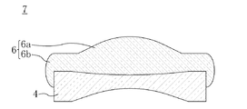
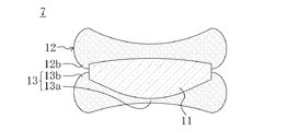
【解決手段】接合光学素子7は、第1光学素子4に対して、第2光学素子素材を加熱しながら押圧することで第2光学素子6を成形することにより、第1光学素子4に第2光学素子6を接合している。第2光学素子6は、素子本体部6aと、素子本体部6aから第1光学素子4の外周面と接触するように延びる接触部6bとを有している。
【選択図】図1
Description
第1及び第2光学素子4,6の外径や厚みは、上記実施形態の値とは異なる任意の値でも良い。さらに、加熱温度、加圧力、及び加圧時間も、上記実施形態の値とは異なる任意の値でも良い。
2 下型
3 胴型
4,9,11,14,17,20,23,26 第1光学素子
5 第2光学素子素材
6,10,12,15,18,24,27 第2光学素子
6a 素子本体部
6b,12b,15b,18b,21b 接触部
7 接合光学素子
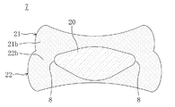
8 外周曲面
13,16,19,22,25 第3光学素子
13a 素子本体部
13b,16b,19b,22b 接触部
28,29 レンズ面
Claims (8)
- 第1光学素子に対して、第2光学素子素材を加熱しながら押圧することで第2光学素子を成形することにより、上記第1光学素子に上記第2光学素子を接合している接合光学素子であって、
上記第2光学素子は、素子本体部と、該素子本体部から上記第1光学素子の外周面と接触するように延びる接触部とを有していることを特徴とする接合光学素子。 - 請求項1記載の接合光学素子において、
上記第1又は第2光学素子に接合されている第3光学素子をさらに備えていることを特徴とする接合光学素子。 - 請求項2記載の接合光学素子において、
上記第2光学素子は、上記第1光学素子の一方の面に接合され、
上記第3光学素子は、上記第1光学素子の他方の面に接合されていて、素子本体部と、該素子本体部から上記第1光学素子の外周面と接触するように延びる接触部とを有していることを特徴とする接合光学素子。 - 請求項3記載の接合光学素子において、
上記第2及び第3光学素子の接触部は、互いに接触又は接合していることを特徴とする接合光学素子。 - 請求項1記載の接合光学素子において、
上記第2光学素子の熱膨張率が上記第1光学素子よりも大きいことを特徴とする接合光学素子。 - 請求項1記載の接合光学素子において、
上記光学素子はガラス製であることを特徴とする接合光学素子。 - 請求項1記載の接合光学素子において、
上記光学素子の接合後に、該光学素子の少なくとも一つが芯取り加工されていることを特徴とする接合光学素子。 - 請求項1記載の接合光学素子において、
上記光学素子の接合面のレンズ面部分が非球面であることを特徴とする接合光学素子。
Priority Applications (2)
| Application Number | Priority Date | Filing Date | Title |
|---|---|---|---|
| JP2007133363A JP2008285377A (ja) | 2007-05-18 | 2007-05-18 | 接合光学素子 |
| US12/121,263 US7746574B2 (en) | 2007-05-18 | 2008-05-15 | Bonded optical element |
Applications Claiming Priority (1)
| Application Number | Priority Date | Filing Date | Title |
|---|---|---|---|
| JP2007133363A JP2008285377A (ja) | 2007-05-18 | 2007-05-18 | 接合光学素子 |
Publications (2)
| Publication Number | Publication Date |
|---|---|
| JP2008285377A true JP2008285377A (ja) | 2008-11-27 |
| JP2008285377A5 JP2008285377A5 (ja) | 2010-03-04 |
Family
ID=40087846
Family Applications (1)
| Application Number | Title | Priority Date | Filing Date |
|---|---|---|---|
| JP2007133363A Pending JP2008285377A (ja) | 2007-05-18 | 2007-05-18 | 接合光学素子 |
Country Status (2)
| Country | Link |
|---|---|
| US (1) | US7746574B2 (ja) |
| JP (1) | JP2008285377A (ja) |
Cited By (2)
| Publication number | Priority date | Publication date | Assignee | Title |
|---|---|---|---|---|
| JP2017049345A (ja) * | 2015-08-31 | 2017-03-09 | 学校法人慶應義塾 | 赤外線レンズ並びにその製造装置及び製造方法 |
| WO2020116132A1 (ja) * | 2018-12-05 | 2020-06-11 | ソニーセミコンダクタソリューションズ株式会社 | 撮像デバイスおよび撮像装置 |
Families Citing this family (3)
| Publication number | Priority date | Publication date | Assignee | Title |
|---|---|---|---|---|
| JP5159621B2 (ja) * | 2006-06-13 | 2013-03-06 | パナソニック株式会社 | 複合レンズおよびその製造方法 |
| JP4728280B2 (ja) * | 2007-05-18 | 2011-07-20 | パナソニック株式会社 | 接合光学素子 |
| DE202010018278U1 (de) * | 2010-01-15 | 2015-05-06 | Schott Ag | Kollimierte Lichtquelle |
Citations (9)
| Publication number | Priority date | Publication date | Assignee | Title |
|---|---|---|---|---|
| JPS4962152A (ja) * | 1972-05-02 | 1974-06-17 | ||
| JPS4973148A (ja) * | 1972-11-13 | 1974-07-15 | ||
| JPS61251466A (ja) * | 1985-03-08 | 1986-11-08 | コルモーゲン コーポレイション | 高エネルギ−強度を有する磁石を用いたサ−ボモ−タ |
| JPS6369732A (ja) * | 1986-09-08 | 1988-03-29 | コ−ニング グラス ワ−クス | モリブデンシ−ル用ガラス |
| JPH05139769A (ja) * | 1991-11-15 | 1993-06-08 | Olympus Optical Co Ltd | 光学部品の組立方法 |
| JP2000313627A (ja) * | 1999-02-22 | 2000-11-14 | Asahi Optical Co Ltd | 光学素子の成形方法 |
| JP2001300944A (ja) * | 2000-04-20 | 2001-10-30 | Sony Corp | 複合レンズの成形方法及び複合レンズ |
| JP2002131511A (ja) * | 2000-10-26 | 2002-05-09 | Sony Corp | 光学素子及び光学素子の製造方法 |
| JP2006171164A (ja) * | 2004-12-14 | 2006-06-29 | Seiko Epson Corp | ハイブリッドレンズ及びハイブリッドレンズの製造方法 |
Family Cites Families (6)
| Publication number | Priority date | Publication date | Assignee | Title |
|---|---|---|---|---|
| JPS6067118A (ja) | 1983-09-24 | 1985-04-17 | Canon Inc | 光学素子の製造方法 |
| US5160361A (en) | 1990-06-13 | 1992-11-03 | Matsushita Electric Industrial Co., Ltd. | Method of manufacturing optical element |
| JP3763552B2 (ja) | 1996-07-30 | 2006-04-05 | Hoya株式会社 | ガラス被覆層を有するガラスレンズ及びその製造方法 |
| DE102005045197B4 (de) | 2005-09-21 | 2010-12-09 | Schott Ag | Verfahren zur Herstellung einer optischen Hybridlinse |
| TWI271546B (en) | 2005-11-29 | 2007-01-21 | Kinik Co | Aspherical designing method for making glass-molding |
| JP2008285375A (ja) | 2007-05-18 | 2008-11-27 | Panasonic Corp | 接合光学素子及びその製造方法 |
-
2007
- 2007-05-18 JP JP2007133363A patent/JP2008285377A/ja active Pending
-
2008
- 2008-05-15 US US12/121,263 patent/US7746574B2/en not_active Expired - Fee Related
Patent Citations (9)
| Publication number | Priority date | Publication date | Assignee | Title |
|---|---|---|---|---|
| JPS4962152A (ja) * | 1972-05-02 | 1974-06-17 | ||
| JPS4973148A (ja) * | 1972-11-13 | 1974-07-15 | ||
| JPS61251466A (ja) * | 1985-03-08 | 1986-11-08 | コルモーゲン コーポレイション | 高エネルギ−強度を有する磁石を用いたサ−ボモ−タ |
| JPS6369732A (ja) * | 1986-09-08 | 1988-03-29 | コ−ニング グラス ワ−クス | モリブデンシ−ル用ガラス |
| JPH05139769A (ja) * | 1991-11-15 | 1993-06-08 | Olympus Optical Co Ltd | 光学部品の組立方法 |
| JP2000313627A (ja) * | 1999-02-22 | 2000-11-14 | Asahi Optical Co Ltd | 光学素子の成形方法 |
| JP2001300944A (ja) * | 2000-04-20 | 2001-10-30 | Sony Corp | 複合レンズの成形方法及び複合レンズ |
| JP2002131511A (ja) * | 2000-10-26 | 2002-05-09 | Sony Corp | 光学素子及び光学素子の製造方法 |
| JP2006171164A (ja) * | 2004-12-14 | 2006-06-29 | Seiko Epson Corp | ハイブリッドレンズ及びハイブリッドレンズの製造方法 |
Cited By (2)
| Publication number | Priority date | Publication date | Assignee | Title |
|---|---|---|---|---|
| JP2017049345A (ja) * | 2015-08-31 | 2017-03-09 | 学校法人慶應義塾 | 赤外線レンズ並びにその製造装置及び製造方法 |
| WO2020116132A1 (ja) * | 2018-12-05 | 2020-06-11 | ソニーセミコンダクタソリューションズ株式会社 | 撮像デバイスおよび撮像装置 |
Also Published As
| Publication number | Publication date |
|---|---|
| US20080297920A1 (en) | 2008-12-04 |
| US7746574B2 (en) | 2010-06-29 |
Similar Documents
| Publication | Publication Date | Title |
|---|---|---|
| JP2008285375A (ja) | 接合光学素子及びその製造方法 | |
| JP4728280B2 (ja) | 接合光学素子 | |
| KR101065577B1 (ko) | 복합렌즈 | |
| US20070195263A1 (en) | Method of manufacturing multifocal lens and multifocal lens | |
| JPH04171401A (ja) | 接合樹脂レンズ | |
| JP2008285377A (ja) | 接合光学素子 | |
| WO2015156315A1 (ja) | レンズ固定方法およびレンズ組立体 | |
| JP2007022905A (ja) | 光学素子デバイスの製造方法、光学素子デバイス、および成形装置 | |
| JP2007304569A (ja) | 接合レンズ及びその製造法 | |
| JP2008285374A (ja) | 接合光学素子及びその製造方法 | |
| JP2014506336A (ja) | ベースレンズおよび膜構造を備えた眼用レンズを製造する方法 | |
| JP2006525889A (ja) | 非球面ハイブリッドレンズの製造方法 | |
| JP2007309964A (ja) | 複合光学素子及びその製造方法 | |
| JP2013033222A (ja) | 回折光学素子及びそれを備えた撮像装置 | |
| JP4744352B2 (ja) | 複合光学素子の製造方法 | |
| WO2016051619A1 (ja) | 光学レンズ | |
| JP2007333859A (ja) | 複合光学素子及びその製造方法 | |
| JP2011167988A (ja) | レンズの製造方法 | |
| JP2004010456A (ja) | 光学素子製造方法、および光学素子 | |
| TWI627447B (zh) | Method for manufacturing optical component | |
| JP3938107B2 (ja) | ハイブリッド成形型 | |
| JP2008129229A (ja) | 複合光学素子および複合光学素子の製造方法 | |
| JP2008015010A (ja) | 複合光学素子及びその製造方法 | |
| JP2003063832A (ja) | 光学素子成形用型 | |
| JP2007125780A (ja) | 成形用型及びその製造方法、熱可塑性素材の成形方法 |
Legal Events
| Date | Code | Title | Description |
|---|---|---|---|
| A521 | Request for written amendment filed |
Free format text: JAPANESE INTERMEDIATE CODE: A523 Effective date: 20100115 |
|
| A621 | Written request for application examination |
Free format text: JAPANESE INTERMEDIATE CODE: A621 Effective date: 20100115 |
|
| A977 | Report on retrieval |
Free format text: JAPANESE INTERMEDIATE CODE: A971007 Effective date: 20110418 |
|
| A131 | Notification of reasons for refusal |
Free format text: JAPANESE INTERMEDIATE CODE: A131 Effective date: 20110426 |
|
| A521 | Request for written amendment filed |
Free format text: JAPANESE INTERMEDIATE CODE: A523 Effective date: 20110623 |
|
| A521 | Request for written amendment filed |
Free format text: JAPANESE INTERMEDIATE CODE: A821 Effective date: 20110623 |
|
| RD02 | Notification of acceptance of power of attorney |
Free format text: JAPANESE INTERMEDIATE CODE: A7422 Effective date: 20120125 |
|
| A131 | Notification of reasons for refusal |
Free format text: JAPANESE INTERMEDIATE CODE: A131 Effective date: 20120306 |
|
| A02 | Decision of refusal |
Free format text: JAPANESE INTERMEDIATE CODE: A02 Effective date: 20120626 |