US7746574B2 - Bonded optical element - Google Patents
Bonded optical element Download PDFInfo
- Publication number
- US7746574B2 US7746574B2 US12/121,263 US12126308A US7746574B2 US 7746574 B2 US7746574 B2 US 7746574B2 US 12126308 A US12126308 A US 12126308A US 7746574 B2 US7746574 B2 US 7746574B2
- Authority
- US
- United States
- Prior art keywords
- optical element
- bonded
- optical
- contact
- face
- Prior art date
- Legal status (The legal status is an assumption and is not a legal conclusion. Google has not performed a legal analysis and makes no representation as to the accuracy of the status listed.)
- Expired - Fee Related, expires
Links
Images


Classifications
-
- G—PHYSICS
- G02—OPTICS
- G02B—OPTICAL ELEMENTS, SYSTEMS OR APPARATUS
- G02B13/00—Optical objectives specially designed for the purposes specified below
- G02B13/001—Miniaturised objectives for electronic devices, e.g. portable telephones, webcams, PDAs, small digital cameras
- G02B13/0055—Miniaturised objectives for electronic devices, e.g. portable telephones, webcams, PDAs, small digital cameras employing a special optical element
- G02B13/0065—Miniaturised objectives for electronic devices, e.g. portable telephones, webcams, PDAs, small digital cameras employing a special optical element having a beam-folding prism or mirror
-
- G—PHYSICS
- G02—OPTICS
- G02B—OPTICAL ELEMENTS, SYSTEMS OR APPARATUS
- G02B13/00—Optical objectives specially designed for the purposes specified below
- G02B13/001—Miniaturised objectives for electronic devices, e.g. portable telephones, webcams, PDAs, small digital cameras
- G02B13/0015—Miniaturised objectives for electronic devices, e.g. portable telephones, webcams, PDAs, small digital cameras characterised by the lens design
- G02B13/002—Miniaturised objectives for electronic devices, e.g. portable telephones, webcams, PDAs, small digital cameras characterised by the lens design having at least one aspherical surface
- G02B13/0025—Miniaturised objectives for electronic devices, e.g. portable telephones, webcams, PDAs, small digital cameras characterised by the lens design having at least one aspherical surface having one lens only
-
- G—PHYSICS
- G02—OPTICS
- G02B—OPTICAL ELEMENTS, SYSTEMS OR APPARATUS
- G02B13/00—Optical objectives specially designed for the purposes specified below
- G02B13/001—Miniaturised objectives for electronic devices, e.g. portable telephones, webcams, PDAs, small digital cameras
- G02B13/0055—Miniaturised objectives for electronic devices, e.g. portable telephones, webcams, PDAs, small digital cameras employing a special optical element
- G02B13/006—Miniaturised objectives for electronic devices, e.g. portable telephones, webcams, PDAs, small digital cameras employing a special optical element at least one element being a compound optical element, e.g. cemented elements
-
- C—CHEMISTRY; METALLURGY
- C03—GLASS; MINERAL OR SLAG WOOL
- C03B—MANUFACTURE, SHAPING, OR SUPPLEMENTARY PROCESSES
- C03B2215/00—Press-moulding glass
- C03B2215/40—Product characteristics
- C03B2215/406—Products comprising at least two different glasses
-
- Y—GENERAL TAGGING OF NEW TECHNOLOGICAL DEVELOPMENTS; GENERAL TAGGING OF CROSS-SECTIONAL TECHNOLOGIES SPANNING OVER SEVERAL SECTIONS OF THE IPC; TECHNICAL SUBJECTS COVERED BY FORMER USPC CROSS-REFERENCE ART COLLECTIONS [XRACs] AND DIGESTS
- Y02—TECHNOLOGIES OR APPLICATIONS FOR MITIGATION OR ADAPTATION AGAINST CLIMATE CHANGE
- Y02P—CLIMATE CHANGE MITIGATION TECHNOLOGIES IN THE PRODUCTION OR PROCESSING OF GOODS
- Y02P40/00—Technologies relating to the processing of minerals
- Y02P40/50—Glass production, e.g. reusing waste heat during processing or shaping
- Y02P40/57—Improving the yield, e-g- reduction of reject rates
Definitions
- the present invention relates to optical elements used for optical systems and the like, such as picture-taking lenses, optical pickups, and the like and especially relates to a bonded optical element in which optical elements different from each other are bonded to each other.
- bonded optical elements in which two or more kinds of lenses or prisms are bonded to each other are manufactured in such a manner that optical elements finished in advance by grinding, polishing, pressing, or the like are bonded to each other by means of an adhesive typified by a UV curing agent.
- This method involves a step of manufacturing each optical element, a positioning step of arranging and positioning the two or more optical elements highly accurately, and a bonding step of applying and curing the adhesive uniformly with air void eliminated, which serve as a bar to increases in accuracy and productivity of the bonded optical elements.
- Patent Document 1 discloses a method for forming a composite optical element in which a first optical element and a second optical element material are disposed between an upper die and a lower die, and the second optical element material is pressed by the dies and the first optical element while being heated at a temperature capable of deforming the second optical element material and incapable of deforming the first element to form a second optical element, thereby integrating the first and second optical elements with each other.
- Patent Document 2 proposes a method of forming a glass lens by directly bonding glasses to each other between which the difference in linear expansion coefficient is in a range between 3 ⁇ 10 ⁇ 7 and 8 ⁇ 10 ⁇ 7 .
- Patent Document 1 Japanese Unexamined Patent Application Publication 60-67118
- Patent Document 2 Japanese Patent No. 3763552
- bonding strength depends on the materials, the forming conditions, the shapes, and the like of optical elements.
- Patent Documents 1 and 2 tried to bond glasses by the methods proposed in Patent Documents 1 and 2 to reach a conclusion that though the glass materials disclosed in the Patent Documents could be bonded to each other, bonding of other glass materials to each other not disclosed therein resulted in insufficient bonding strength in some cases and in no attainment of bonding of glass materials to each other in other cases. This means that the bonding strength is ignored in Patent Documents 1 and 2.
- the present invention has been made in view of the foregoing and has its object of maintaining the bonding strength at a high level.
- a bonded optical element in accordance with the present invention includes a first optical element and a second optical element bonded to each other by forming the second optical element by heating and pressing against the first optical element a second optical element material, wherein the second optical element includes an element body part and a contact part extending from the element body part to be in contact with an outer peripheral face of the first optical element.
- the bonding strength can be maintained at a high level.
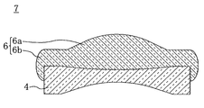
- FIG. 1 is a sectional view of a bonded optical element in accordance with an embodiment of the present invention.
- FIG. 2 presents schematic sectional views showing a bonded optical element manufacturing method, wherein FIG. 2( a ) shows a state in which formation of a second optical element is prepared and FIG. 2( b ) shows a state in which formation of the second optical element is completed.
- FIG. 3 is a sectional view of a bonded optical element in which a first optical element and a second optical element are a spherical biconvex lens and a spherical biconcave lens, respectively.
- FIG. 4 is a sectional view of a bonded optical element in which a second optical element and a third optical element are bonded to and integrated with the upper face and the lower face of a first optical element, respectively.
- FIG. 5 is a sectional view of a bonded optical element in which a second optical element and a third optical element are bonded to and integrated with the upper face and the lower face of a first optical element, respectively.
- FIG. 6 is a sectional view of a bonded optical element in which a second optical element and a third optical element are bonded to and integrated with the upper face and the lower face of a first optical element, respectively.
- FIG. 7 is a sectional view of a bonded optical element in which a second optical element and a third optical element are bonded to and integrated with the upper face and the lower face of a first optical element, respectively.
- FIG. 8 is a sectional view of a bonded optical element in which only second and third optical elements are subjected to centering.
- FIG. 9 is a sectional view of a bonded optical element of which lens face parts of the bonded faces are aspheric.
- FIG. 1 is a sectional view of a bonded optical element 7 in accordance with the present embodiment.
- the bonded optical element 7 includes first and second optical elements 4 , 6 .
- the first optical element 4 is a spherical biconcave lens having an outer diameter of 10 mm, a center thickness of 2 mm, and an edge thickness of 4 mm.
- the first optical element 4 is made of a material, VC79 (a product by Sumida Optical Glass Inc.) having a refractive index nd of 1.60970, an Abbe number vd of 57.8, a glass transition temperature (transition temperature) Tg of 561° C., a glass softening temperature (a flexure temperature) At of 553° C., and a coefficient ⁇ of thermal expansion of 93 ⁇ 10 ⁇ 6 .
- the first optical element 4 is formed by polishing.
- the second optical element 6 is bonded directly to the upper face of the first optical element 4 to be integrated therewith.
- the second optical element 6 is a spherical biconvex lens having an outer diameter of 14 mm, a center thickness of 4 mm, and an edge thickness of 2 mm. Namely, the outer diameter of the second optical element 6 is larger than that of the first optical element 4 .
- the second optical element 6 includes an element body part 6 a arranged on the upper face of the first optical element 4 and a contact part 6 b extending downward from the outer edge (the outer periphery) of the element body part 6 a so as to be in contact with the outer peripheral face of the first optical element 4 .
- the contact part 6 b is formed so as to extend up to the substantial center in the thickness direction of the edge portion of the first optical element 4 around the entire periphery of the outer edge of the element body part 6 a and is in contact with the entire periphery of the upper part of the outer peripheral face of the first optical element 4 .
- the contact part 6 a calks the first optical element 4 .
- the second optical element 6 is made of a material, CD45 (a product by Sumida Optical Glass Inc.) having a refractive index nd of 1.69320, an Abbe number vd of 33.7, a glass transition temperature Tg of 470° C., a glass softening temperature At of 507° C., and a coefficient ⁇ of thermal expansion of 110 ⁇ 10 ⁇ 6 .
- the glass softening temperature At of the second optical element 6 is lower than the glass transition temperature Tg and the glass softening temperature At of the first optical element 4 , and the coefficient ⁇ of thermal expansion of the second optical element 6 is larger than that of the first optical element 4 .
- FIG. 2 presents schematic sectional views showing the method for manufacturing the bonded optical element 7 , wherein FIG. 2( a ) shows a state in which formation of the second optical element is prepared and FIG. 2( b ) shows a state in which formation of the second optical element is completed.
- the first optical element 4 and a second optical element material 5 are prepared.
- the outer diameter of the first optical element material 5 is smaller than the inner diameter of a sleeve die 3 , as shown in FIG. 2 . Accordingly, a space is formed between the outer peripheral face of the first optical element 4 and the inner peripheral face of the sleeve die 3 .
- the outer diameter of the second optical element material 5 is smaller than that of the first optical element 4 .
- a lower die 2 is inserted into the sleeve die 3 , and the first optical element 4 is put on the lower die 2 .
- the second optical element material 5 is put on the first optical element 4 , and then, an upper die 1 is inserted into the sleeve die 3 so as to be placed on the second optical element material 5 .
- the centers of the upper die 1 and the lower die 2 are aligned with each other.
- the second optical element material 5 is pressed against the first optical element 4 while being heated at a temperature incapable of deforming the first optical element 4 and capable of deforming the second optical element material 5 so that the outer diameter of the second optical element 6 becomes larger than that of the first optical element 4 .
- the heating temperature is 525° C.
- the applied pressure is 200 kgf/cm 2
- the pressing period of time is 60 seconds.
- the second optical element 6 is formed, as shown in FIG. 2( b ).
- the second optical element material 5 gets into the space to form the contact part 6 b , as shown in FIG. 2( b ).
- the bonded optical element 7 is formed in which the second optical element 6 is bonded to and integrated with the upper face of the first optical element 4 .
- the thus obtained bonded optical element 7 of which second optical element 6 is in contact with the outer peripheral face of the first optical element 4 , has sufficient bonding strength and is excellent in quality with no breakage, no crack, and no opacity.
- the second optical element 6 includes the element body part 6 a and the contact part 6 b extending from the element body part 6 a so as to be in contact with the outer peripheral face of the first optical element 4 , thereby maintaining the bonding strength at a high level.
- the second optical element 6 having a coefficient of thermal expansion larger than that of the first optical element 4
- compression stress at the contact part 6 b of the second optical element 6 works on the outer peripheral face of the first optical element 4 in cooling after application of heat and pressure to the second optical element material 5 , thereby increasing the bonding strength further.
- the compression stress can be obtained by setting the temperature of the second optical element material 5 higher than that of the first optical element 4 in application of heat and pressure to the second optical element material 5 .
- each of the first and second optical elements 4 , 6 may be arbitrary values different from the values in the above embodiment.
- the hating temperature, the applied pressure, the pressing period of time may be arbitrary values different from the values in the above embodiment.
- the contact part 6 b is formed around the entire periphery of the outer edge of the element body part 6 a in the above embodiment, but the range where the contact part 6 b is formed may be any range as long as it is formed at at least a part of the outer edge of the element body part 6 a . Wherein, the contact part 6 b is preferably formed around the entire periphery of the outer edge of the element body part 6 a.
- the contact part 6 b is in contact with the upper part of the outer peripheral face of the first optical element 4 in the above embodiment, but its contact range may be any range as long as it is in contact with at least a part in the thickness direction of the outer peripheral face of the first optical element 4 .
- first optical element 4 and the second optical element 6 are a spherical biconcave lens and a spherical biconvex lens, respectively, in the above invention, but the present invention is not limited thereto.
- a first optical element 10 and a second optical element 11 may a spherical biconvex lens and a spherical biconcave lens, respectively, as shown in FIG. 3 .
- one or both of the faces opposite to the bonded faces of the first and second optical elements may be aspheric.
- the first optical element 4 is formed by polishing in the above embodiment, but the present invention is not limited thereto and the first optical element may be formed by press forming, for example.
- a third optical element may be further provided which is bonded to and integrated with the first or second optical element.
- a second optical element 12 and a third optical element 13 may be directly bonded to and integrated with the upper face (one of the faces) and the lower face (the other face) of a first optical element 11 , respectively, by the same manner as in the above embodiment.
- the third optical element 13 has almost the same structure as the second optical element 6 .
- the third optical element 13 includes an element body part 13 a arranged on the lower face of the first optical element 11 and a contact part 13 b extending upward from the outer edge of the element main body 13 a so as to be in contact with the outer peripheral face of the first optical element 11 .
- the contact parts 12 b , 13 b of the second and third optical elements 12 , 13 are out of contact with each other.
- the second and third optical elements 12 , 13 may be formed simultaneously or separately.
- a second optical element 15 and a third optical element 16 made of a material different from that of the second optical element 15 may be directly bonded to and integrated with the upper face and the lower face of a first optical element 14 , respectively, by the same manner as in the above embodiment so that the contact parts 15 b , 16 b of the second and third optical elements 15 , 16 are in contact with each other.
- the first optical element 14 may be enclosed by the second and third optical elements 15 , 16 .
- the second and third optical elements 15 , 16 may be formed simultaneously or separately.
- a second optical element 18 and a third optical element 19 made of the same material as that of the second optical element 18 may be directly bonded to and integrated with the upper face and the lower face of a first optical element 17 , respectively, by the same manner as in the above embodiment so that the contact parts 18 b , 19 b of the second and third optical elements 18 , 19 are bonded to and integrated with each other.
- the first optical element 17 may be enclosed by the second and third optical elements 18 , 19 .
- the second and third optical elements 18 , 19 are formed simultaneously.
- a second optical element 21 and a third optical element 22 made of the same material as that of the second optical element 21 may be directly and respectively bonded to and integrated with the upper face and the lower face of a first optical element 20 , which is a spherical biconvex lens having a curved outer peripheral face 8 substantially in an R shape in section protruding radially outward, by the same manner as in the above embodiment so that the contact parts 21 b , 22 b of the second and third optical elements 21 , 22 are bonded to and integrated with each other.
- the first optical element 20 may be enclosed by the second and third optical elements 21 , 22 .
- the second and third optical elements 21 , 22 are formed simultaneously.
- the first and second optical elements 4 , 6 are made of the aforementioned glass materials in the above embodiment, but the present invention is not limited thereto and they may be made of glass materials different from the glass materials in the above embodiment or may be made of plastic. Wherein, the first and second optical elements 4 , 6 are preferably made of glass materials.
- the glass-made first and second optical elements 4 , 6 bring the bonded optical element 7 to have a highly accurate form, high heat resistance, high mechanical durability, and high homogeneity. The same is applicable to the aforementioned bonded optical element 7 including the third optical element.
- At least one of the optical elements may be centered after bonding and integrating the optical elements.
- first to third optical elements 23 to 25 after first to third optical elements 23 to 25 are bonded to and integrated with one another, only the second and third optical elements 24 , 25 may be centered.
- only one of the second and third optical elements 24 , 25 may be centered, or all of the first to third optical elements 23 to 25 may be centered. Centering in this way improves the eccentricity accuracy of the bonded optical element 7 .
- the first optical element 4 is a spherical lens in the above embodiment, but a lens face part (an optically functioning face part) 28 of the bonded face of a first optical element 26 to a second optical element 27 may be aspheric, as shown in FIG. 9 .
- a lens face part 29 of the bonded face of the second optical element 27 to the first optical element 26 is aspheric also.
- Each of the lens face parts 28 , 29 which include the optically effective face, is a curved face ranging up to the upper face (the edge face) of the edge portion.
- the aspheric lens face parts 28 , 29 of the bonded faces of the bonded optical element 7 lead to an improvement on the degree of freedom in designing an optical system, thereby leading to multifunction and compaction of an optical system.
- the lens face part 28 thereof can be easily formed so as to be aspheric. The same is applicable to the aforementioned bonded optical element 7 including the third optical element.
- the present invention is not limited to the above embodiments and can be reduced in practice in various ways without deviating from the sprit and the main subject matter of the present invention.
- the present invention is applicable for the purpose of maintaining the bonding strength at a high level and the like.
Applications Claiming Priority (2)
| Application Number | Priority Date | Filing Date | Title |
|---|---|---|---|
| JP2007133363A JP2008285377A (ja) | 2007-05-18 | 2007-05-18 | 接合光学素子 |
| JP2007-133363 | 2007-05-18 |
Publications (2)
| Publication Number | Publication Date |
|---|---|
| US20080297920A1 US20080297920A1 (en) | 2008-12-04 |
| US7746574B2 true US7746574B2 (en) | 2010-06-29 |
Family
ID=40087846
Family Applications (1)
| Application Number | Title | Priority Date | Filing Date |
|---|---|---|---|
| US12/121,263 Expired - Fee Related US7746574B2 (en) | 2007-05-18 | 2008-05-15 | Bonded optical element |
Country Status (2)
| Country | Link |
|---|---|
| US (1) | US7746574B2 (ja) |
| JP (1) | JP2008285377A (ja) |
Families Citing this family (5)
| Publication number | Priority date | Publication date | Assignee | Title |
|---|---|---|---|---|
| US8111470B2 (en) * | 2006-06-13 | 2012-02-07 | Panasonic Corporation | Composite lens and method for manufacturing the same |
| JP4728280B2 (ja) * | 2007-05-18 | 2011-07-20 | パナソニック株式会社 | 接合光学素子 |
| DE202010018278U1 (de) * | 2010-01-15 | 2015-05-06 | Schott Ag | Kollimierte Lichtquelle |
| JP2017049345A (ja) * | 2015-08-31 | 2017-03-09 | 学校法人慶應義塾 | 赤外線レンズ並びにその製造装置及び製造方法 |
| JP2020091385A (ja) * | 2018-12-05 | 2020-06-11 | ソニーセミコンダクタソリューションズ株式会社 | 撮像デバイスおよび撮像装置 |
Citations (8)
| Publication number | Priority date | Publication date | Assignee | Title |
|---|---|---|---|---|
| JPS6067118A (ja) | 1983-09-24 | 1985-04-17 | Canon Inc | 光学素子の製造方法 |
| US5160361A (en) | 1990-06-13 | 1992-11-03 | Matsushita Electric Industrial Co., Ltd. | Method of manufacturing optical element |
| JPH1045419A (ja) | 1996-07-30 | 1998-02-17 | Hoya Corp | ガラス被覆層を有するガラスレンズ及びその製造方法 |
| US6551530B2 (en) * | 2000-04-20 | 2003-04-22 | Sony Corporation | Method of forming a hybrid lens |
| JP2006171164A (ja) * | 2004-12-14 | 2006-06-29 | Seiko Epson Corp | ハイブリッドレンズ及びハイブリッドレンズの製造方法 |
| US20070091472A1 (en) | 2005-09-21 | 2007-04-26 | Jochen Alkemper | Optical lens or lens group, process for the production thereof, as well as optical image acquisition device |
| US20070119212A1 (en) | 2005-11-29 | 2007-05-31 | Kinik Company | Axial symmetric molding glass lens, mold assembly for an axial symmetric molding glass lens, method for manufacturing a mold assembly for an axial symmetric molding glass lens and method for manufacturing an axial symmetric molding glass lens |
| US20080285154A1 (en) | 2007-05-18 | 2008-11-20 | Tetsuya Suzuki | Bonded optical element and manufacturing method thereof |
Family Cites Families (7)
| Publication number | Priority date | Publication date | Assignee | Title |
|---|---|---|---|---|
| DE2221488B2 (de) * | 1972-05-02 | 1975-06-19 | Fa. Carl Zeiss, 7920 Heidenheim | Verfahren zur Herstellung von phototropen Mehrstärkenbrillengläsern |
| JPS4973148A (ja) * | 1972-11-13 | 1974-07-15 | ||
| US4679313A (en) * | 1985-03-08 | 1987-07-14 | Kollmorgen Technologies Corporation | Method of making a servo motor with high energy product magnets |
| US4693987A (en) * | 1986-09-08 | 1987-09-15 | Corning Glass Works | Molybdenum sealing glasses |
| JPH05139769A (ja) * | 1991-11-15 | 1993-06-08 | Olympus Optical Co Ltd | 光学部品の組立方法 |
| JP2000313627A (ja) * | 1999-02-22 | 2000-11-14 | Asahi Optical Co Ltd | 光学素子の成形方法 |
| JP2002131511A (ja) * | 2000-10-26 | 2002-05-09 | Sony Corp | 光学素子及び光学素子の製造方法 |
-
2007
- 2007-05-18 JP JP2007133363A patent/JP2008285377A/ja active Pending
-
2008
- 2008-05-15 US US12/121,263 patent/US7746574B2/en not_active Expired - Fee Related
Patent Citations (9)
| Publication number | Priority date | Publication date | Assignee | Title |
|---|---|---|---|---|
| JPS6067118A (ja) | 1983-09-24 | 1985-04-17 | Canon Inc | 光学素子の製造方法 |
| US5160361A (en) | 1990-06-13 | 1992-11-03 | Matsushita Electric Industrial Co., Ltd. | Method of manufacturing optical element |
| JPH1045419A (ja) | 1996-07-30 | 1998-02-17 | Hoya Corp | ガラス被覆層を有するガラスレンズ及びその製造方法 |
| JP3763552B2 (ja) | 1996-07-30 | 2006-04-05 | Hoya株式会社 | ガラス被覆層を有するガラスレンズ及びその製造方法 |
| US6551530B2 (en) * | 2000-04-20 | 2003-04-22 | Sony Corporation | Method of forming a hybrid lens |
| JP2006171164A (ja) * | 2004-12-14 | 2006-06-29 | Seiko Epson Corp | ハイブリッドレンズ及びハイブリッドレンズの製造方法 |
| US20070091472A1 (en) | 2005-09-21 | 2007-04-26 | Jochen Alkemper | Optical lens or lens group, process for the production thereof, as well as optical image acquisition device |
| US20070119212A1 (en) | 2005-11-29 | 2007-05-31 | Kinik Company | Axial symmetric molding glass lens, mold assembly for an axial symmetric molding glass lens, method for manufacturing a mold assembly for an axial symmetric molding glass lens and method for manufacturing an axial symmetric molding glass lens |
| US20080285154A1 (en) | 2007-05-18 | 2008-11-20 | Tetsuya Suzuki | Bonded optical element and manufacturing method thereof |
Non-Patent Citations (6)
| Title |
|---|
| Related U.S. Appl. No. 12/121,125, filed May 15, 2008. |
| Related U.S. Appl. No. 12/121,155, filed May 15, 2008. |
| Related U.S. Appl. No. 12/121,227, filed May 15, 2008. |
| United States Office Action issued in related U.S. Appl. No. 12/121,125, dated Nov. 3, 2009. |
| United States Office Action issued in related U.S. Appl. No. 12/121,155, dated Sep. 18, 2009. |
| United States Office Action issued in related U.S. Appl. No. 12/121,227, dated Nov. 3, 2009. |
Also Published As
| Publication number | Publication date |
|---|---|
| JP2008285377A (ja) | 2008-11-27 |
| US20080297920A1 (en) | 2008-12-04 |
Similar Documents
| Publication | Publication Date | Title |
|---|---|---|
| US7885018B2 (en) | Bonded optical element and manufacturing method thereof | |
| US7764446B2 (en) | Bonded optical element | |
| US7746574B2 (en) | Bonded optical element | |
| US20070195263A1 (en) | Method of manufacturing multifocal lens and multifocal lens | |
| US20080055736A1 (en) | Optical element and production device for producing same | |
| US7746573B2 (en) | Bonded optical element and manufacturing method thereof | |
| US7796337B2 (en) | Optical microstructure plate and fabrication mold thereof | |
| JP2007304569A (ja) | 接合レンズ及びその製造法 | |
| US20210129466A1 (en) | Optical element and method for manufacturing the same | |
| CN112218832B (zh) | 玻璃透镜成型模具 | |
| JP4777265B2 (ja) | 熱成形により光学部品を製造する方法および装置 | |
| JP5504376B2 (ja) | スタック型ウエハアセンブリのための精密スペーシング | |
| JP2022093460A (ja) | ガラスレンズ成形型 | |
| JP2006525889A (ja) | 非球面ハイブリッドレンズの製造方法 | |
| JP4744352B2 (ja) | 複合光学素子の製造方法 | |
| JP5161525B2 (ja) | 光学素子の成形方法 | |
| JP5112120B2 (ja) | 光学素子の製造方法とその製造用金型組立体 | |
| JP2004010456A (ja) | 光学素子製造方法、および光学素子 | |
| KR20190091194A (ko) | 유리제 성형형 | |
| KR20220079146A (ko) | 비등온 성형 공정을 이용한 양면 비구면 렌즈의 제조방법. | |
| KR20120061419A (ko) | 렌즈 어레이 모듈 및 이의 성형방법 | |
| JP2006126336A (ja) | レンズ及びその製造方法 | |
| JP2009096648A (ja) | レンズアレイの製造方法 | |
| JP2002274869A (ja) | 光学素子成形型および光学素子成形方法 | |
| JP2008241816A (ja) | 光学素子およびその製造方法 |
Legal Events
| Date | Code | Title | Description |
|---|---|---|---|
| AS | Assignment |
Owner name: MATSUSHITA ELECTRIC INDUSTRIAL CO., LTD., JAPAN Free format text: ASSIGNMENT OF ASSIGNORS INTEREST;ASSIGNORS:SUZUKI, TETSUYA;TOKUNAGA, TOMOKAZU;REEL/FRAME:021549/0184 Effective date: 20080714 Owner name: MATSUSHITA ELECTRIC INDUSTRIAL CO., LTD.,JAPAN Free format text: ASSIGNMENT OF ASSIGNORS INTEREST;ASSIGNORS:SUZUKI, TETSUYA;TOKUNAGA, TOMOKAZU;REEL/FRAME:021549/0184 Effective date: 20080714 |
|
| AS | Assignment |
Owner name: PANASONIC CORPORATION, JAPAN Free format text: CHANGE OF NAME;ASSIGNOR:MATSUSHITA ELECTRIC INDUSTRIAL CO., LTD.;REEL/FRAME:021832/0197 Effective date: 20081001 Owner name: PANASONIC CORPORATION,JAPAN Free format text: CHANGE OF NAME;ASSIGNOR:MATSUSHITA ELECTRIC INDUSTRIAL CO., LTD.;REEL/FRAME:021832/0197 Effective date: 20081001 |
|
| FEPP | Fee payment procedure |
Free format text: PAYOR NUMBER ASSIGNED (ORIGINAL EVENT CODE: ASPN); ENTITY STATUS OF PATENT OWNER: LARGE ENTITY |
|
| REMI | Maintenance fee reminder mailed | ||
| LAPS | Lapse for failure to pay maintenance fees | ||
| STCH | Information on status: patent discontinuation |
Free format text: PATENT EXPIRED DUE TO NONPAYMENT OF MAINTENANCE FEES UNDER 37 CFR 1.362 |
|
| FP | Lapsed due to failure to pay maintenance fee |
Effective date: 20140629 |