JP2008285377A - Joined optical element - Google Patents
Joined optical element Download PDFInfo
- Publication number
- JP2008285377A JP2008285377A JP2007133363A JP2007133363A JP2008285377A JP 2008285377 A JP2008285377 A JP 2008285377A JP 2007133363 A JP2007133363 A JP 2007133363A JP 2007133363 A JP2007133363 A JP 2007133363A JP 2008285377 A JP2008285377 A JP 2008285377A
- Authority
- JP
- Japan
- Prior art keywords
- optical element
- optical
- bonded
- joined
- contact
- Prior art date
- Legal status (The legal status is an assumption and is not a legal conclusion. Google has not performed a legal analysis and makes no representation as to the accuracy of the status listed.)
- Pending
Links
Images


Classifications
-
- G—PHYSICS
- G02—OPTICS
- G02B—OPTICAL ELEMENTS, SYSTEMS OR APPARATUS
- G02B13/00—Optical objectives specially designed for the purposes specified below
- G02B13/001—Miniaturised objectives for electronic devices, e.g. portable telephones, webcams, PDAs, small digital cameras
- G02B13/0055—Miniaturised objectives for electronic devices, e.g. portable telephones, webcams, PDAs, small digital cameras employing a special optical element
- G02B13/0065—Miniaturised objectives for electronic devices, e.g. portable telephones, webcams, PDAs, small digital cameras employing a special optical element having a beam-folding prism or mirror
-
- G—PHYSICS
- G02—OPTICS
- G02B—OPTICAL ELEMENTS, SYSTEMS OR APPARATUS
- G02B13/00—Optical objectives specially designed for the purposes specified below
- G02B13/001—Miniaturised objectives for electronic devices, e.g. portable telephones, webcams, PDAs, small digital cameras
- G02B13/0015—Miniaturised objectives for electronic devices, e.g. portable telephones, webcams, PDAs, small digital cameras characterised by the lens design
- G02B13/002—Miniaturised objectives for electronic devices, e.g. portable telephones, webcams, PDAs, small digital cameras characterised by the lens design having at least one aspherical surface
- G02B13/0025—Miniaturised objectives for electronic devices, e.g. portable telephones, webcams, PDAs, small digital cameras characterised by the lens design having at least one aspherical surface having one lens only
-
- G—PHYSICS
- G02—OPTICS
- G02B—OPTICAL ELEMENTS, SYSTEMS OR APPARATUS
- G02B13/00—Optical objectives specially designed for the purposes specified below
- G02B13/001—Miniaturised objectives for electronic devices, e.g. portable telephones, webcams, PDAs, small digital cameras
- G02B13/0055—Miniaturised objectives for electronic devices, e.g. portable telephones, webcams, PDAs, small digital cameras employing a special optical element
- G02B13/006—Miniaturised objectives for electronic devices, e.g. portable telephones, webcams, PDAs, small digital cameras employing a special optical element at least one element being a compound optical element, e.g. cemented elements
-
- C—CHEMISTRY; METALLURGY
- C03—GLASS; MINERAL OR SLAG WOOL
- C03B—MANUFACTURE, SHAPING, OR SUPPLEMENTARY PROCESSES
- C03B2215/00—Press-moulding glass
- C03B2215/40—Product characteristics
- C03B2215/406—Products comprising at least two different glasses
-
- Y—GENERAL TAGGING OF NEW TECHNOLOGICAL DEVELOPMENTS; GENERAL TAGGING OF CROSS-SECTIONAL TECHNOLOGIES SPANNING OVER SEVERAL SECTIONS OF THE IPC; TECHNICAL SUBJECTS COVERED BY FORMER USPC CROSS-REFERENCE ART COLLECTIONS [XRACs] AND DIGESTS
- Y02—TECHNOLOGIES OR APPLICATIONS FOR MITIGATION OR ADAPTATION AGAINST CLIMATE CHANGE
- Y02P—CLIMATE CHANGE MITIGATION TECHNOLOGIES IN THE PRODUCTION OR PROCESSING OF GOODS
- Y02P40/00—Technologies relating to the processing of minerals
- Y02P40/50—Glass production, e.g. reusing waste heat during processing or shaping
- Y02P40/57—Improving the yield, e-g- reduction of reject rates
Abstract
Description
本発明は、撮影レンズや光ピックアップなどの光学系等に使用される光学素子、特に、互いに異なる光学素子同士を接合している接合光学素子に関するものである。 The present invention relates to an optical element used in an optical system such as a photographing lens and an optical pickup, and more particularly to a bonded optical element in which different optical elements are bonded to each other.
従来、2種類以上のレンズやプリズムなどを接合した接合光学素子は、予め研削・研磨加工やプレス加工などによって仕上げられた光学素子同士を紫外線硬化型に代表される接着剤で接合して製造されている。しかしながら、この方法では、それぞれの光学素子を製造する工程や、2種類以上の光学素子を高精度に位置決めして配置する位置決め工程や、接着剤を気泡の無い状態で均一に塗布して硬化する接着工程が必要であり、接合光学素子の精度向上と生産性向上の障害となっている。 Conventionally, a bonded optical element in which two or more kinds of lenses and prisms are bonded is manufactured by bonding optical elements that have been previously finished by grinding, polishing, pressing, or the like with an adhesive typified by an ultraviolet curing type. ing. However, in this method, the process of manufacturing each optical element, the positioning process of positioning and arranging two or more types of optical elements with high accuracy, and the adhesive is uniformly applied and cured without bubbles. An adhesion process is required, which is an obstacle to improving the accuracy and productivity of the bonded optical element.
これに対して、上記位置決め工程と上記接着工程を無くすことを目的として、硝材同士の融着接合により接合光学素子を成形する方法が提案されている。 On the other hand, for the purpose of eliminating the positioning step and the bonding step, a method of forming a bonded optical element by fusion bonding of glass materials has been proposed.
例えば、特許文献1には、上下の型の間に第1光学素子と第2光学素子素材を配置し、第2光学素子素材が変形可能でかつ第1光学素子が変形不可能な温度で加熱しながら、型と第1光学素子により第2光学素子素材をプレス加工して第2光学素子を成形し、第1と第2光学素子を一体化して合成光学素子を成形する方法が開示されている。
For example, in
また、特許文献2には、冷却時間を短縮してもクラックが生じることのないようにするため、互いの線膨張係数の差が3×10⁻⁷〜8×10⁻⁷であるガラス同士を直接接合してガラスレンズを成形する方法が提案されている。
ところで、接合光学素子を形成する上で、接合強度を高くすることは必須である。そして、接合強度は、光学素子の材質や成形条件、形状などに影響される。 By the way, in forming the bonded optical element, it is essential to increase the bonding strength. The bonding strength is affected by the material, molding conditions, shape, etc. of the optical element.
しかしながら、本発明者たちがガラス同士の接合を特許文献1及び2の方法で試みると、それらの特許文献に示されたガラスだと接合するが、そこに記載のない他の硝材だと接合強度が十分でない場合や、さらには、そもそも接合しない場合もあることが明らかになった。つまり、特許文献1及び2では、接合強度に関してはほとんど鑑みられていない。
However, when the present inventors try to join the glasses with the methods of
本発明は、かかる点に鑑みてなされたものであり、その目的とするところは、接合強度を高いレベルで維持することにある。 This invention is made | formed in view of this point, The place made into the objective is to maintain joining strength at a high level.
本発明に係る接合光学素子は、第1光学素子に対して、第2光学素子素材を加熱しながら押圧することで第2光学素子を成形することにより、上記第1光学素子に上記第2光学素子を接合している接合光学素子であって、上記第2光学素子は、素子本体部と、該素子本体部から上記第1光学素子の外周面と接触するように延びる接触部とを有していることを特徴とするものである。 In the bonding optical element according to the present invention, the second optical element is formed on the first optical element by molding the second optical element by pressing the second optical element material while heating the first optical element. A bonded optical element for bonding elements, wherein the second optical element has an element main body and a contact portion extending from the element main body so as to be in contact with the outer peripheral surface of the first optical element. It is characterized by that.
本発明によれば、接合強度を高いレベルで維持できる。 According to the present invention, the bonding strength can be maintained at a high level.
以下、本発明の実施形態を図面に基づいて詳細に説明する。 Hereinafter, embodiments of the present invention will be described in detail with reference to the drawings.
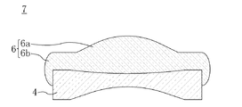
図1は、本実施形態に係る接合光学素子7の断面図である。図1に示すように、この接合光学素子7は、第1及び第2光学素子4,6を備えている。この第1光学素子4は、外径が10mm、中心厚みが2mm、コバ部の厚みが4mmの球面両凹レンズである。第1光学素子4の材料は、屈折率ndが1.60970、アッベ数νdが57.8、ガラス転移温度(転移点温度)Tgが516℃、ガラス軟化温度(屈伏点温度)Atが553℃、熱膨張率αが93×10−6のVC79((株)住田光学ガラス製)である。そして、第1光学素子4は、研磨加工により成形されている。
FIG. 1 is a cross-sectional view of the bonded
第2光学素子6は、第1光学素子4の上面に直接接合されて一体化されている。第2光学素子6は、外径が14mm、中心厚みが4mm、コバ部の厚みが2mmの球面両凸レンズである。つまり、第2光学素子6の外径は、第1光学素子4よりも大きい。第2光学素子6は、第1光学素子4の上面に配置された素子本体部6aと、この素子本体部6aの外縁(外周)から第1光学素子4の外周面と接触するように下側に延びる接触部6bとを有している。この接触部6bは、具体的には、素子本体部6aの外縁の全周に亘って第1光学素子4のコバ部の厚み方向略中央まで延伸するように形成されていて、第1光学素子4の外周面の上部と全周に亘って接触している。これにより、接触部6bが第1光学素子4をかしめている。
The second
第2光学素子6の材料は、屈性率ndが1.69320、アッベ数νdが33.7、ガラス転移温度Tgが470℃、ガラス軟化温度Atが507℃、熱膨張率αが110×10−6のCD45((株)住田光学ガラス製)である。つまり、第2光学素子6のガラス軟化温度Atは、第1光学素子4のガラス転移温度Tg及びガラス軟化温度Atよりも低く、第2光学素子6の熱膨張率αは、第1光学素子4よりも大きい。
The material of the second
以下、図2を参照しながら、接合光学素子7の製造方法について説明する。図2は、接合光学素子7の製造工程を示す概略断面図であり、(a)は、第2光学素子成形準備段階を示す図であり、(b)は、第2光学素子成形完了段階を示す図である。
Hereinafter, a method for manufacturing the cemented
まず、第1光学素子4及び第2光学素子素材5を用意する。この第1光学素子4の外径は、図2(a)に示すように、胴型3の内径よりも小さい。つまり、第1光学素子4の外周面と胴型3の内周面との間に隙間がある。第2光学素子素材5の外径は、第1光学素子4よりも小さい。
First, the first
それから、胴型3に下型2を挿入し、下型2上に第1光学素子4を置く。次に、第1光学素子4上に第2光学素子素材5を置く。その後、上型1を胴型3に挿入して第2光学素子素材5上に置く。このように胴型3に上型1及び下型2を挿入することにより、上型1及び下型2の互いの中心位置を合わす。
Then, the
そして、上型1、下型2、及び胴型3により、第1光学素子4に対して、第2光学素子素材5を第1光学素子4が変形不可能でかつ第2光学素子素材5が変形可能な温度で加熱しながら第2光学素子6の外径が第1光学素子4よりも大きくなるように押圧する。本実施形態では、加熱温度は525℃、加圧力は200kgf/cm2、加圧時間は60秒である。これにより、図2(b)に示すように、第2光学素子6が成形される。
The
ここで、上述のように、第1光学素子4の外周面と胴型3の内周面との間に空間があるので、図2(b)に示すように、第2光学素子素材5がその空間に回り込み、接触部6bが成形される。
Here, as described above, since there is a space between the outer peripheral surface of the first
以上により、第1光学素子4の上面に第2光学素子6が接合されて一体化された接合光学素子7が成形される。このようにして得られる接合光学素子7は、第1光学素子4の外周面に第2光学素子6が接触していて、接合強度が十分で、割れやクラック、曇りの発生も無く、品質の良いものである。
As described above, the joined
以上のように、本実施形態によれば、第2光学素子6は、素子本体部6aと、この素子本体部6aから第1光学素子4の外周面と接触するように延びる接触部6bとを有していることにより、接合強度を高いレベルで維持できる。
As described above, according to the present embodiment, the second
また、第2光学素子6の熱膨張率が第1光学素子4よりも大きいことにより、第2光学素子素材5の加熱・加圧後の冷却時において第1光学素子4の外周面に第2光学素子6の接触部6bからの圧縮応力が働き、その接合強度がさらに強くなる。なお、上記圧縮応力を働かせるためには、このように、第2光学素子6の熱膨張率を第1光学素子4よりも大きくするのが効果的であるが、これに限らず、第2光学素子素材5の加熱・加圧時において第2光学素子素材5の温度を第1光学素子4よりも高くしても、上記圧縮応力を得ることができる。
Further, since the thermal expansion coefficient of the second
一方、第1光学素子4の外周面に第2光学素子6が接触しないように、上記接合成形を試みた。そうすると、その接合強度が弱く、接合光学素子7を形成することができなかった。このことにより、第1光学素子4の外周面に第2光学素子6を接触させることで、接合光学素子7を形成できると言える。
On the other hand, the above-described bonding molding was attempted so that the second
(その他の実施形態)
第1及び第2光学素子4,6の外径や厚みは、上記実施形態の値とは異なる任意の値でも良い。さらに、加熱温度、加圧力、及び加圧時間も、上記実施形態の値とは異なる任意の値でも良い。
(Other embodiments)
The outer diameters and thicknesses of the first and second
また、上記実施形態では、接触部6bを素子本体部6aの外縁の全周に亘って形成しているが、素子本体部6aの外縁の少なくとも一部に形成する限り、その形成範囲の如何は問わない。但し、接触部6bを素子本体部6aの外縁の全周に亘って形成するのが望ましい。
Moreover, in the said embodiment, although the
また、上記実施形態では、接触部6bは第1光学素子4の外周面の上部と接触しているが、第1光学素子4の外周面の厚み方向の少なくとも一部と接触する限り、その接触範囲の如何は問わない。
Moreover, in the said embodiment, although the
また、上記実施形態では、第1光学素子4が球面両凹レンズ、第2光学素子6が球面両凸レンズであるが、これに限らず、例えば、図3に示すように、第1光学素子10が球面両凸レンズ、第2光学素子11が球面両凹レンズであっても良い。さらに、第1及び/又は第2光学素子の、接合面とは反対側の面が、非球面であっても良い。
In the above embodiment, the first
また、上記実施形態では、第1光学素子4を研磨加工により形成しているが、これに限らず、例えば、第1光学素子をプレス成形により形成しても良い。
In the above-described embodiment, the first
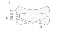
また、上記実施形態では、第1又は第2光学素子に接合されて一体化されている第3光学素子をさらに備えていても良い。例えば、図4に示すように、第1光学素子11の上面(一方の面)に第2光学素子12を、第1光学素子11の下面(他方の面)に第3光学素子13を、それぞれ上記実施形態と同様の方法で直接接合して一体化しても良い。この第3光学素子13は、第2光学素子12とほぼ同様の構成である。つまり、第3光学素子13は、第1光学素子4の下面に配置された素子本体部13aと、この素子本体部13aの外縁から第1光学素子4の外周面と接触するように上側に延びる接触部13bとを有している。そして、第2及び第3光学素子12,13の接触部12b,13bは、互いに非接触状態である。この場合、第2及び第3光学素子12,13を同時に形成しても、別々に形成しても良い。
Moreover, in the said embodiment, you may further provide the 3rd optical element joined and integrated with the 1st or 2nd optical element. For example, as shown in FIG. 4, the second
さらに、図5に示すように、第1光学素子14の上面に第2光学素子15を、第1光学素子14の下面に第2光学素子15の材料とは異なる材料からなる第3光学素子16を、それぞれ上記実施形態と同様の方法で直接接合して一体化し、第2及び第3光学素子15,16の接触部15b,16bを互いに接触させても良い。つまり、第1光学素子14を第2及び第3光学素子15,16で包み込んでも良い。この場合、第2及び第3光学素子15,16を同時に形成しても、別々に形成しても良い。
Further, as shown in FIG. 5, the second
その上、図6に示すように、第1光学素子17の上面に第2光学素子18を、第1光学素子17の下面に第2光学素子18の材料と同じ材料からなる第3光学素子19を、それぞれ上記実施形態と同様の方法で直接接合して一体化し、第2及び第3光学素子18,19の接触部18b,19bを互いに接合して一体化させても良い。つまり、第1光学素子17を第2及び第3光学素子18,19で包み込んでも良い。この場合、第2及び第3光学素子18,19を同時に形成する。
In addition, as shown in FIG. 6, the second
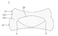
それに加えて、図7に示すように、第1光学素子20として、断面形状が径方向外側に突出する略R形状の外周曲面8を有する球面両凸レンズを用意し、第1光学素子20の上面に第2光学素子21を、第1光学素子20の下面に第2光学素子21の材料と同じ材料からなる第3光学素子22を、それぞれ上記実施形態と同様の方法で直接接合して一体化し、、第2及び第3光学素子21,22の接触部21b,22bを互いに接合して一体化しても良い。つまり、第1光学素子20を第2及び第3光学素子21,22で包み込んでも良い。この場合、第2及び第3光学素子21,22を同時に形成する。このように、第1光学素子20の外周曲面8の断面形状が略R形状であることにより、第1〜第3光学素子20〜22の接合により割れやクラックが発生するのを抑制できる。
In addition, as shown in FIG. 7, a spherical biconvex lens having a substantially R-shaped outer peripheral
また、上記実施形態では、第1及び第2光学素子4,6はガラス製であるが、これに限らず、例えば、上記実施形態のガラス材料とは異なるガラス材料からなるものであったり、プラスチック製であったりしても良い。但し、第1及び第2光学素子4,6はガラス製であるのが望ましい。このようにガラス製であることにより、接合光学素子7において、高い形状精度、高い耐熱性、高い機械的耐久性、高い均質性を実現できる。なお、以上と同様のことは、上記した、第3光学素子を備えた接合光学素子7についても当てはまる。
Moreover, in the said embodiment, although the 1st and 2nd
また、上記実施形態では、光学素子の接合・一体化後に、その光学素子の少なくとも一つが芯取り加工されていても良い。例えば、図8に示すように、第1〜第3光学素子23〜25の接合・一体化後に、第2及び第3光学素子24,25のみ芯取り加工しても良い。さらに、第2又は第3光学素子24,25のみ芯取り加工しても、全部23〜25を芯取り加工しても良い。このように芯取り加工することにより、接合光学素子7の偏心精度を向上させることができる。
In the above embodiment, after the optical elements are joined and integrated, at least one of the optical elements may be centered. For example, as shown in FIG. 8, after the first to third
また、上記実施形態では、第1光学素子4が球面レンズであるが、図9に示すように、第1光学素子26の、第2光学素子27との接合面のレンズ面(光学機能面)28部分を非球面としても良い。この場合、第2光学素子27の、第1光学素子26との接合面のレンズ面29部分も非球面となる。これらのレンズ面28,29は、光学有効面を含む、コバ部の上面(コバ面)までの曲面である。このように接合光学素子7の接合面のレンズ面28,29部分を非球面とすることにより、光学システム設計の自由度を向上させることができ、光学システムの高機能化、コンパクト化などを実現できる。ここで、第1光学素子26をプレス成形により形成する場合、そのレンズ面28を容易に非球面とすることができる。なお、以上と同様のことは、上記した、第3光学素子を備えた接合光学素子7についても当てはまる。
Moreover, in the said embodiment, although the 1st
本発明は、実施形態に限定されず、その精神又は主要な特徴から逸脱することなく他の色々な形で実施することができる。 The present invention is not limited to the embodiments, and can be implemented in various other forms without departing from the spirit or main features thereof.
このように、上述の実施形態はあらゆる点で単なる例示に過ぎず、限定的に解釈してはならない。本発明の範囲は特許請求の範囲によって示すものであって、明細書には何ら拘束されない。さらに、特許請求の範囲の均等範囲に属する変形や変更は、全て本発明の範囲内のものである。 As described above, the above-described embodiment is merely an example in all respects and should not be interpreted in a limited manner. The scope of the present invention is defined by the claims, and is not limited by the specification. Further, all modifications and changes belonging to the equivalent scope of the claims are within the scope of the present invention.
以上説明したように、本発明は、接合強度を高いレベルで維持するための用途等について適用できる。 As described above, the present invention can be applied to applications for maintaining the bonding strength at a high level.
1 上型
2 下型
3 胴型
4,9,11,14,17,20,23,26 第1光学素子
5 第2光学素子素材
6,10,12,15,18,24,27 第2光学素子
6a 素子本体部
6b,12b,15b,18b,21b 接触部
7 接合光学素子
8 外周曲面
13,16,19,22,25 第3光学素子
13a 素子本体部
13b,16b,19b,22b 接触部
28,29 レンズ面
DESCRIPTION OF
Claims (8)
上記第2光学素子は、素子本体部と、該素子本体部から上記第1光学素子の外周面と接触するように延びる接触部とを有していることを特徴とする接合光学素子。 A bonded optical element in which the second optical element is bonded to the first optical element by molding the second optical element by pressing the second optical element material while heating the first optical element. Because
The second optical element includes an element main body and a contact portion extending from the element main body so as to be in contact with the outer peripheral surface of the first optical element.
上記第1又は第2光学素子に接合されている第3光学素子をさらに備えていることを特徴とする接合光学素子。 The bonded optical element according to claim 1,
A joined optical element, further comprising a third optical element joined to the first or second optical element.
上記第2光学素子は、上記第1光学素子の一方の面に接合され、
上記第3光学素子は、上記第1光学素子の他方の面に接合されていて、素子本体部と、該素子本体部から上記第1光学素子の外周面と接触するように延びる接触部とを有していることを特徴とする接合光学素子。 The bonded optical element according to claim 2,
The second optical element is bonded to one surface of the first optical element,
The third optical element is bonded to the other surface of the first optical element, and includes an element main body portion and a contact portion extending from the element main body portion so as to contact the outer peripheral surface of the first optical element. A cemented optical element comprising:
上記第2及び第3光学素子の接触部は、互いに接触又は接合していることを特徴とする接合光学素子。 In the bonded optical element according to claim 3,
The contact portion of the second and third optical elements is in contact with or bonded to each other.
上記第2光学素子の熱膨張率が上記第1光学素子よりも大きいことを特徴とする接合光学素子。 The bonded optical element according to claim 1,
A cemented optical element, wherein the second optical element has a coefficient of thermal expansion greater than that of the first optical element.
上記光学素子はガラス製であることを特徴とする接合光学素子。 The bonded optical element according to claim 1,
The bonding optical element, wherein the optical element is made of glass.
上記光学素子の接合後に、該光学素子の少なくとも一つが芯取り加工されていることを特徴とする接合光学素子。 The bonded optical element according to claim 1,
A cemented optical element, wherein at least one of the optical elements is centered after the optical elements are joined.
上記光学素子の接合面のレンズ面部分が非球面であることを特徴とする接合光学素子。 The bonded optical element according to claim 1,
A cemented optical element, wherein a lens surface portion of the cemented surface of the optical element is an aspherical surface.
Priority Applications (2)
| Application Number | Priority Date | Filing Date | Title |
|---|---|---|---|
| JP2007133363A JP2008285377A (en) | 2007-05-18 | 2007-05-18 | Joined optical element |
| US12/121,263 US7746574B2 (en) | 2007-05-18 | 2008-05-15 | Bonded optical element |
Applications Claiming Priority (1)
| Application Number | Priority Date | Filing Date | Title |
|---|---|---|---|
| JP2007133363A JP2008285377A (en) | 2007-05-18 | 2007-05-18 | Joined optical element |
Publications (2)
| Publication Number | Publication Date |
|---|---|
| JP2008285377A true JP2008285377A (en) | 2008-11-27 |
| JP2008285377A5 JP2008285377A5 (en) | 2010-03-04 |
Family
ID=40087846
Family Applications (1)
| Application Number | Title | Priority Date | Filing Date |
|---|---|---|---|
| JP2007133363A Pending JP2008285377A (en) | 2007-05-18 | 2007-05-18 | Joined optical element |
Country Status (2)
| Country | Link |
|---|---|
| US (1) | US7746574B2 (en) |
| JP (1) | JP2008285377A (en) |
Cited By (2)
| Publication number | Priority date | Publication date | Assignee | Title |
|---|---|---|---|---|
| JP2017049345A (en) * | 2015-08-31 | 2017-03-09 | 学校法人慶應義塾 | Infrared lens, and apparatus and method of manufacturing the same |
| WO2020116132A1 (en) * | 2018-12-05 | 2020-06-11 | ソニーセミコンダクタソリューションズ株式会社 | Imaging device and imaging system |
Families Citing this family (3)
| Publication number | Priority date | Publication date | Assignee | Title |
|---|---|---|---|---|
| JP5159621B2 (en) * | 2006-06-13 | 2013-03-06 | パナソニック株式会社 | Compound lens and manufacturing method thereof |
| JP4728280B2 (en) * | 2007-05-18 | 2011-07-20 | パナソニック株式会社 | Bonding optical element |
| DE202010018278U1 (en) * | 2010-01-15 | 2015-05-06 | Schott Ag | Collimated light source |
Citations (9)
| Publication number | Priority date | Publication date | Assignee | Title |
|---|---|---|---|---|
| JPS4962152A (en) * | 1972-05-02 | 1974-06-17 | ||
| JPS4973148A (en) * | 1972-11-13 | 1974-07-15 | ||
| JPS61251466A (en) * | 1985-03-08 | 1986-11-08 | コルモーゲン コーポレイション | Servo motor using magnet having high energy intensity |
| JPS6369732A (en) * | 1986-09-08 | 1988-03-29 | コ−ニング グラス ワ−クス | Glass for sealing molybdenum |
| JPH05139769A (en) * | 1991-11-15 | 1993-06-08 | Olympus Optical Co Ltd | Method for assembling optical parts |
| JP2000313627A (en) * | 1999-02-22 | 2000-11-14 | Asahi Optical Co Ltd | Method for molding optical element |
| JP2001300944A (en) * | 2000-04-20 | 2001-10-30 | Sony Corp | Method for molding composite lens, and composite lens |
| JP2002131511A (en) * | 2000-10-26 | 2002-05-09 | Sony Corp | Optical element and method for manufacturing the same |
| JP2006171164A (en) * | 2004-12-14 | 2006-06-29 | Seiko Epson Corp | Hybrid lens and method of manufacturing hybrid lens |
Family Cites Families (6)
| Publication number | Priority date | Publication date | Assignee | Title |
|---|---|---|---|---|
| JPS6067118A (en) | 1983-09-24 | 1985-04-17 | Canon Inc | Manufacture of optical element |
| US5160361A (en) | 1990-06-13 | 1992-11-03 | Matsushita Electric Industrial Co., Ltd. | Method of manufacturing optical element |
| JP3763552B2 (en) | 1996-07-30 | 2006-04-05 | Hoya株式会社 | Glass lens having glass coating layer and manufacturing method thereof |
| DE102005045197B4 (en) | 2005-09-21 | 2010-12-09 | Schott Ag | Process for producing a hybrid optical lens |
| TWI271546B (en) | 2005-11-29 | 2007-01-21 | Kinik Co | Aspherical designing method for making glass-molding |
| JP2008285375A (en) | 2007-05-18 | 2008-11-27 | Panasonic Corp | Joined optical element and its manufacturing method |
-
2007
- 2007-05-18 JP JP2007133363A patent/JP2008285377A/en active Pending
-
2008
- 2008-05-15 US US12/121,263 patent/US7746574B2/en not_active Expired - Fee Related
Patent Citations (9)
| Publication number | Priority date | Publication date | Assignee | Title |
|---|---|---|---|---|
| JPS4962152A (en) * | 1972-05-02 | 1974-06-17 | ||
| JPS4973148A (en) * | 1972-11-13 | 1974-07-15 | ||
| JPS61251466A (en) * | 1985-03-08 | 1986-11-08 | コルモーゲン コーポレイション | Servo motor using magnet having high energy intensity |
| JPS6369732A (en) * | 1986-09-08 | 1988-03-29 | コ−ニング グラス ワ−クス | Glass for sealing molybdenum |
| JPH05139769A (en) * | 1991-11-15 | 1993-06-08 | Olympus Optical Co Ltd | Method for assembling optical parts |
| JP2000313627A (en) * | 1999-02-22 | 2000-11-14 | Asahi Optical Co Ltd | Method for molding optical element |
| JP2001300944A (en) * | 2000-04-20 | 2001-10-30 | Sony Corp | Method for molding composite lens, and composite lens |
| JP2002131511A (en) * | 2000-10-26 | 2002-05-09 | Sony Corp | Optical element and method for manufacturing the same |
| JP2006171164A (en) * | 2004-12-14 | 2006-06-29 | Seiko Epson Corp | Hybrid lens and method of manufacturing hybrid lens |
Cited By (2)
| Publication number | Priority date | Publication date | Assignee | Title |
|---|---|---|---|---|
| JP2017049345A (en) * | 2015-08-31 | 2017-03-09 | 学校法人慶應義塾 | Infrared lens, and apparatus and method of manufacturing the same |
| WO2020116132A1 (en) * | 2018-12-05 | 2020-06-11 | ソニーセミコンダクタソリューションズ株式会社 | Imaging device and imaging system |
Also Published As
| Publication number | Publication date |
|---|---|
| US20080297920A1 (en) | 2008-12-04 |
| US7746574B2 (en) | 2010-06-29 |
Similar Documents
| Publication | Publication Date | Title |
|---|---|---|
| JP2008285375A (en) | Joined optical element and its manufacturing method | |
| JP4728280B2 (en) | Bonding optical element | |
| KR101065577B1 (en) | Compound lens | |
| US20070195263A1 (en) | Method of manufacturing multifocal lens and multifocal lens | |
| JPH04171401A (en) | Junction resin lens | |
| JP2008285377A (en) | Joined optical element | |
| WO2015156315A1 (en) | Lens securing method and lens assembly | |
| JP2007022905A (en) | Optical element device manufacturing method, optical element device and forming apparatus | |
| JP2007304569A (en) | Compound lens and manufacture method thereof | |
| JP2008285374A (en) | Joined optical element and its manufacturing method | |
| JP2014506336A (en) | Method for manufacturing ophthalmic lens with base lens and membrane structure | |
| JP2006525889A (en) | Manufacturing method of aspherical hybrid lens | |
| JP2007309964A (en) | Complex optical element and method of manufacturing the same | |
| JP2013033222A (en) | Diffractive optical element and imaging apparatus using the same | |
| JP4744352B2 (en) | Method for manufacturing composite optical element | |
| WO2016051619A1 (en) | Optical lens | |
| JP2007333859A (en) | Compound optical element and its manufacturing method | |
| JP2011167988A (en) | Method for manufacturing lens | |
| JP2004010456A (en) | Manufacturing method of optical element and optical element | |
| TWI627447B (en) | Method for manufacturing optical component | |
| JP3938107B2 (en) | Hybrid mold | |
| JP2008129229A (en) | Composite optical element and method of manufacturing composite optical element | |
| JP2008015010A (en) | Compound optical element and its manufacturing method | |
| JP2003063832A (en) | Mold for forming optical element | |
| JP2007125780A (en) | Mold, method for producing mold, and method for molding thermoplastic material |
Legal Events
| Date | Code | Title | Description |
|---|---|---|---|
| A521 | Request for written amendment filed |
Free format text: JAPANESE INTERMEDIATE CODE: A523 Effective date: 20100115 |
|
| A621 | Written request for application examination |
Free format text: JAPANESE INTERMEDIATE CODE: A621 Effective date: 20100115 |
|
| A977 | Report on retrieval |
Free format text: JAPANESE INTERMEDIATE CODE: A971007 Effective date: 20110418 |
|
| A131 | Notification of reasons for refusal |
Free format text: JAPANESE INTERMEDIATE CODE: A131 Effective date: 20110426 |
|
| A521 | Request for written amendment filed |
Free format text: JAPANESE INTERMEDIATE CODE: A523 Effective date: 20110623 |
|
| A521 | Request for written amendment filed |
Free format text: JAPANESE INTERMEDIATE CODE: A821 Effective date: 20110623 |
|
| RD02 | Notification of acceptance of power of attorney |
Free format text: JAPANESE INTERMEDIATE CODE: A7422 Effective date: 20120125 |
|
| A131 | Notification of reasons for refusal |
Free format text: JAPANESE INTERMEDIATE CODE: A131 Effective date: 20120306 |
|
| A02 | Decision of refusal |
Free format text: JAPANESE INTERMEDIATE CODE: A02 Effective date: 20120626 |