JP2008102017A - 基板検査装置 - Google Patents
基板検査装置 Download PDFInfo
- Publication number
- JP2008102017A JP2008102017A JP2006284747A JP2006284747A JP2008102017A JP 2008102017 A JP2008102017 A JP 2008102017A JP 2006284747 A JP2006284747 A JP 2006284747A JP 2006284747 A JP2006284747 A JP 2006284747A JP 2008102017 A JP2008102017 A JP 2008102017A
- Authority
- JP
- Japan
- Prior art keywords
- prober frame
- load lock
- substrate
- lock chamber
- stocker
- Prior art date
- Legal status (The legal status is an assumption and is not a legal conclusion. Google has not performed a legal analysis and makes no representation as to the accuracy of the status listed.)
- Granted
Links
Images


Classifications
-
- G—PHYSICS
- G02—OPTICS
- G02F—OPTICAL DEVICES OR ARRANGEMENTS FOR THE CONTROL OF LIGHT BY MODIFICATION OF THE OPTICAL PROPERTIES OF THE MEDIA OF THE ELEMENTS INVOLVED THEREIN; NON-LINEAR OPTICS; FREQUENCY-CHANGING OF LIGHT; OPTICAL LOGIC ELEMENTS; OPTICAL ANALOGUE/DIGITAL CONVERTERS
- G02F1/00—Devices or arrangements for the control of the intensity, colour, phase, polarisation or direction of light arriving from an independent light source, e.g. switching, gating or modulating; Non-linear optics
- G02F1/01—Devices or arrangements for the control of the intensity, colour, phase, polarisation or direction of light arriving from an independent light source, e.g. switching, gating or modulating; Non-linear optics for the control of the intensity, phase, polarisation or colour
- G02F1/13—Devices or arrangements for the control of the intensity, colour, phase, polarisation or direction of light arriving from an independent light source, e.g. switching, gating or modulating; Non-linear optics for the control of the intensity, phase, polarisation or colour based on liquid crystals, e.g. single liquid crystal display cells
- G02F1/1306—Details
- G02F1/1309—Repairing; Testing
-
- G—PHYSICS
- G01—MEASURING; TESTING
- G01R—MEASURING ELECTRIC VARIABLES; MEASURING MAGNETIC VARIABLES
- G01R31/00—Arrangements for testing electric properties; Arrangements for locating electric faults; Arrangements for electrical testing characterised by what is being tested not provided for elsewhere
- G01R31/28—Testing of electronic circuits, e.g. by signal tracer
- G01R31/302—Contactless testing
-
- G—PHYSICS
- G02—OPTICS
- G02F—OPTICAL DEVICES OR ARRANGEMENTS FOR THE CONTROL OF LIGHT BY MODIFICATION OF THE OPTICAL PROPERTIES OF THE MEDIA OF THE ELEMENTS INVOLVED THEREIN; NON-LINEAR OPTICS; FREQUENCY-CHANGING OF LIGHT; OPTICAL LOGIC ELEMENTS; OPTICAL ANALOGUE/DIGITAL CONVERTERS
- G02F1/00—Devices or arrangements for the control of the intensity, colour, phase, polarisation or direction of light arriving from an independent light source, e.g. switching, gating or modulating; Non-linear optics
- G02F1/01—Devices or arrangements for the control of the intensity, colour, phase, polarisation or direction of light arriving from an independent light source, e.g. switching, gating or modulating; Non-linear optics for the control of the intensity, phase, polarisation or colour
- G02F1/13—Devices or arrangements for the control of the intensity, colour, phase, polarisation or direction of light arriving from an independent light source, e.g. switching, gating or modulating; Non-linear optics for the control of the intensity, phase, polarisation or colour based on liquid crystals, e.g. single liquid crystal display cells
- G02F1/1303—Apparatus specially adapted to the manufacture of LCDs
-
- G—PHYSICS
- G09—EDUCATION; CRYPTOGRAPHY; DISPLAY; ADVERTISING; SEALS
- G09G—ARRANGEMENTS OR CIRCUITS FOR CONTROL OF INDICATING DEVICES USING STATIC MEANS TO PRESENT VARIABLE INFORMATION
- G09G3/00—Control arrangements or circuits, of interest only in connection with visual indicators other than cathode-ray tubes
- G09G3/006—Electronic inspection or testing of displays and display drivers, e.g. of LED or LCD displays
-
- G—PHYSICS
- G02—OPTICS
- G02F—OPTICAL DEVICES OR ARRANGEMENTS FOR THE CONTROL OF LIGHT BY MODIFICATION OF THE OPTICAL PROPERTIES OF THE MEDIA OF THE ELEMENTS INVOLVED THEREIN; NON-LINEAR OPTICS; FREQUENCY-CHANGING OF LIGHT; OPTICAL LOGIC ELEMENTS; OPTICAL ANALOGUE/DIGITAL CONVERTERS
- G02F1/00—Devices or arrangements for the control of the intensity, colour, phase, polarisation or direction of light arriving from an independent light source, e.g. switching, gating or modulating; Non-linear optics
- G02F1/01—Devices or arrangements for the control of the intensity, colour, phase, polarisation or direction of light arriving from an independent light source, e.g. switching, gating or modulating; Non-linear optics for the control of the intensity, phase, polarisation or colour
- G02F1/13—Devices or arrangements for the control of the intensity, colour, phase, polarisation or direction of light arriving from an independent light source, e.g. switching, gating or modulating; Non-linear optics for the control of the intensity, phase, polarisation or colour based on liquid crystals, e.g. single liquid crystal display cells
- G02F1/133—Constructional arrangements; Operation of liquid crystal cells; Circuit arrangements
- G02F1/136—Liquid crystal cells structurally associated with a semi-conducting layer or substrate, e.g. cells forming part of an integrated circuit
- G02F1/1362—Active matrix addressed cells
- G02F1/136254—Checking; Testing
Landscapes
- Physics & Mathematics (AREA)
- Nonlinear Science (AREA)
- General Physics & Mathematics (AREA)
- Engineering & Computer Science (AREA)
- Optics & Photonics (AREA)
- Chemical & Material Sciences (AREA)
- Crystallography & Structural Chemistry (AREA)
- Manufacturing & Machinery (AREA)
- General Engineering & Computer Science (AREA)
- Computer Hardware Design (AREA)
- Theoretical Computer Science (AREA)
- Container, Conveyance, Adherence, Positioning, Of Wafer (AREA)
- Testing Electric Properties And Detecting Electric Faults (AREA)
- Liquid Crystal (AREA)
- Analysing Materials By The Use Of Radiation (AREA)
- Testing Or Measuring Of Semiconductors Or The Like (AREA)
Abstract
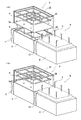
【解決手段】基板検査装置1は、真空状態で基板の検査を行うメインチャンバ2と、大気側との間及びメインチャンバとの間で基板の搬出入を行うロードロックチャンバ3と、基板と電気的に接触して検査信号を印加するプローバフレーム20を格納するプローバフレームストッカ4とを備え、このプローバフレームストッカ4をロードロックチャンバ3あるいはメインチャンバ2の上部に配置する。プローバフレームストッカ4をロードロックチャンバ3上又はメインチャンバ2上に配置する構成とすることで、プローバフレームストッカ4の据え付けに要する面積は、ロードロックチャンバ3又はメインチャンバ2の据え付け面積をそのまま利用することができ、据え付け面積の増大を防ぐことができる。
【選択図】図1
Description
Claims (7)
- 真空状態で基板に検査信号を印加して基板検査を行う基板検査装置において、
真空状態で基板の検査を行うメインチャンバと、
大気側との間及び前記メインチャンバとの間で基板の搬出入を行うロードロックチャンバと、
基板と電気的に接触して検査信号を印加するプローバフレームを格納するプローバフレームストッカとを備え、
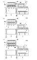
前記プローバフレームストッカを前記ロードロックチャンバの上部に配置したことを特徴とする、基板検査装置。 - 前記ロードロックチャンバは開閉自在の天板を有し、
前記天板は、上部に前記プローバフレームストッカを、下部に前記プローブフレームを搬送する搬送機構を備え、
前記天板及びプローバフレームストッカを昇降自在とする昇降機構を備え、
前記昇降機構の昇降動作と前記搬送機構の搬送動作により、ロードロックチャンバとプローバフレームストッカとの間でプローバフレームの交換を行うことを特徴とする、請求項1に記載の基板検査装置。 - 前記メインチャンバの上部にプローバフレームを一時的に保持する仮置き部を備え、
前記搬送機構はプローバフレームストッカとの間のプローバフレームの交換を前記仮置き部を介して行うことを特徴とする、請求項2に記載の基板検査装置。 - 前記昇降機構は、昇降動作により前記プローバフレームストッカと前記仮置き部との位置合わせを行うことを特徴とする、請求項3に記載の基板検査装置。
- 真空状態で基板に検査信号を印加して基板検査を行う基板検査装置において、
真空状態で基板の検査を行うメインチャンバと、
大気側との間及び前記メインチャンバとの間で基板の搬出入を行うロードロックチャンバと、
基板と電気的に接触して検査信号を印加するプローバフレームを格納するプローバフレームストッカとを備え、
前記プローバフレームストッカを前記メインチャンバの上部に配置したことを特徴とする、基板検査装置。 - 前記ロードロックチャンバは開閉自在の天板を有し、
前記天板は、下部に前記プローブフレームを搬送する搬送機構を備え、
前記天板を昇降自在とする昇降機構を備え、
前記昇降機構の昇降動作と前記搬送機構の搬送動作により、ロードロックチャンバとプローバフレームストッカとの間でプローバフレームの交換を行うことを特徴とする、請求項5に記載の基板検査装置。 - 前記昇降機構は、昇降動作により前記プローバフレームストッカと前記搬送機構との位置合わせを行うことを特徴とする、請求項6に記載の基板検査装置。
Priority Applications (4)
| Application Number | Priority Date | Filing Date | Title |
|---|---|---|---|
| JP2006284747A JP4941645B2 (ja) | 2006-10-19 | 2006-10-19 | 基板検査装置 |
| CN2007101235502A CN101165546B (zh) | 2006-10-19 | 2007-07-02 | 基板检查装置 |
| KR1020070066414A KR100813868B1 (ko) | 2006-10-19 | 2007-07-03 | 기판 검사 장치 |
| TW096124669A TWI342390B (en) | 2006-10-19 | 2007-07-06 | Substrate inspecting apparatus |
Applications Claiming Priority (1)
| Application Number | Priority Date | Filing Date | Title |
|---|---|---|---|
| JP2006284747A JP4941645B2 (ja) | 2006-10-19 | 2006-10-19 | 基板検査装置 |
Publications (2)
| Publication Number | Publication Date |
|---|---|
| JP2008102017A true JP2008102017A (ja) | 2008-05-01 |
| JP4941645B2 JP4941645B2 (ja) | 2012-05-30 |
Family
ID=39334297
Family Applications (1)
| Application Number | Title | Priority Date | Filing Date |
|---|---|---|---|
| JP2006284747A Expired - Fee Related JP4941645B2 (ja) | 2006-10-19 | 2006-10-19 | 基板検査装置 |
Country Status (4)
| Country | Link |
|---|---|
| JP (1) | JP4941645B2 (ja) |
| KR (1) | KR100813868B1 (ja) |
| CN (1) | CN101165546B (ja) |
| TW (1) | TWI342390B (ja) |
Cited By (1)
| Publication number | Priority date | Publication date | Assignee | Title |
|---|---|---|---|---|
| JP2010271655A (ja) * | 2009-05-25 | 2010-12-02 | Shimadzu Corp | プローバフレーム搬送台車およびプローバフレームハンドリングシステム |
Families Citing this family (2)
| Publication number | Priority date | Publication date | Assignee | Title |
|---|---|---|---|---|
| CN103698630B (zh) * | 2013-12-12 | 2016-04-06 | 合肥京东方光电科技有限公司 | 一种电学阵列检测设备 |
| JP2016023939A (ja) * | 2014-07-16 | 2016-02-08 | セイコーエプソン株式会社 | 電子部品搬送装置および電子部品検査装置 |
Citations (3)
| Publication number | Priority date | Publication date | Assignee | Title |
|---|---|---|---|---|
| JP2004233141A (ja) * | 2003-01-29 | 2004-08-19 | Shimadzu Corp | 液晶基板検査装置 |
| JP2005227263A (ja) * | 2004-02-12 | 2005-08-25 | Applied Materials Inc | 集積基板搬送モジュールを備えた電子ビームテストシステム |
| JP2005233997A (ja) * | 2004-02-17 | 2005-09-02 | Shimadzu Corp | 液晶基板検査装置 |
Family Cites Families (3)
| Publication number | Priority date | Publication date | Assignee | Title |
|---|---|---|---|---|
| US5982190A (en) * | 1998-02-04 | 1999-11-09 | Toro-Lira; Guillermo L. | Method to determine pixel condition on flat panel displays using an electron beam |
| JP4676681B2 (ja) * | 2003-06-10 | 2011-04-27 | 株式会社島津製作所 | Tftアレイ検査装置、及びtftアレイ検査方法 |
| JP4147587B2 (ja) * | 2004-03-22 | 2008-09-10 | 株式会社島津製作所 | 基板検査装置 |
-
2006
- 2006-10-19 JP JP2006284747A patent/JP4941645B2/ja not_active Expired - Fee Related
-
2007
- 2007-07-02 CN CN2007101235502A patent/CN101165546B/zh not_active Expired - Fee Related
- 2007-07-03 KR KR1020070066414A patent/KR100813868B1/ko not_active IP Right Cessation
- 2007-07-06 TW TW096124669A patent/TWI342390B/zh not_active IP Right Cessation
Patent Citations (3)
| Publication number | Priority date | Publication date | Assignee | Title |
|---|---|---|---|---|
| JP2004233141A (ja) * | 2003-01-29 | 2004-08-19 | Shimadzu Corp | 液晶基板検査装置 |
| JP2005227263A (ja) * | 2004-02-12 | 2005-08-25 | Applied Materials Inc | 集積基板搬送モジュールを備えた電子ビームテストシステム |
| JP2005233997A (ja) * | 2004-02-17 | 2005-09-02 | Shimadzu Corp | 液晶基板検査装置 |
Cited By (1)
| Publication number | Priority date | Publication date | Assignee | Title |
|---|---|---|---|---|
| JP2010271655A (ja) * | 2009-05-25 | 2010-12-02 | Shimadzu Corp | プローバフレーム搬送台車およびプローバフレームハンドリングシステム |
Also Published As
| Publication number | Publication date |
|---|---|
| CN101165546B (zh) | 2010-09-29 |
| JP4941645B2 (ja) | 2012-05-30 |
| TW200819737A (en) | 2008-05-01 |
| KR100813868B1 (ko) | 2008-03-17 |
| TWI342390B (en) | 2011-05-21 |
| CN101165546A (zh) | 2008-04-23 |
Similar Documents
| Publication | Publication Date | Title |
|---|---|---|
| KR101854015B1 (ko) | 프로브 카드 수납 장치 | |
| JP7009340B2 (ja) | 成膜装置、成膜方法、及び電子デバイスの製造方法 | |
| JP2007003517A (ja) | 統合されたプローバドライブを備えた基板支持部 | |
| JP2020141121A (ja) | アライメント装置、成膜装置、アライメント方法、成膜方法、電子デバイスの製造方法、記録媒体、及びプログラム | |
| JP5555757B2 (ja) | 基板検査装置 | |
| JP4941645B2 (ja) | 基板検査装置 | |
| KR20150061529A (ko) | 디스플레이 셀들을 검사하기 위한 장치 | |
| KR20180135580A (ko) | 턴오버 방식의 디스플레이 셀 검사장치 및 그 제어방법 | |
| KR20200034576A (ko) | 기판 처리 장치 | |
| JP2006317437A (ja) | インライン電子ビーム検査システム | |
| JP2010016066A (ja) | 基板検査装置 | |
| KR20200049314A (ko) | 흡착 및 얼라인먼트 방법, 흡착 시스템, 성막 방법, 성막 장치 및 전자 디바이스의 제조 방법 | |
| KR101322164B1 (ko) | 디스플레이 셀들을 검사하기 위한 장치 | |
| KR101535726B1 (ko) | 디스플레이 셀들을 검사하기 위한 장치 | |
| JP4147587B2 (ja) | 基板検査装置 | |
| TW202025365A (zh) | 基板處理裝置及搬送位置修正方法 | |
| JP2007183541A (ja) | 液晶パネル検査装置 | |
| JP5527715B2 (ja) | 基板検査装置 | |
| JP2012220617A (ja) | プロキシミティ露光装置、及びプロキシミティ露光装置のマスク搬送方法 | |
| KR20070039667A (ko) | 표시패널의 검사장치 및 이의 검사방법 | |
| JP3119098U (ja) | Tftアレイ検査装置 | |
| KR101009808B1 (ko) | 검사 장치, 검사 방법 및 기억 매체 | |
| KR100971944B1 (ko) | 자외선을 이용하는 기판세정장치 | |
| JP2005335836A (ja) | Tftアレイ検査装置 | |
| JP5392945B2 (ja) | プロキシミティ露光装置、及びプロキシミティ露光装置の負圧室の天板搬送方法 |
Legal Events
| Date | Code | Title | Description |
|---|---|---|---|
| A621 | Written request for application examination |
Free format text: JAPANESE INTERMEDIATE CODE: A621 Effective date: 20081212 |
|
| A977 | Report on retrieval |
Free format text: JAPANESE INTERMEDIATE CODE: A971007 Effective date: 20120127 |
|
| TRDD | Decision of grant or rejection written | ||
| A01 | Written decision to grant a patent or to grant a registration (utility model) |
Free format text: JAPANESE INTERMEDIATE CODE: A01 Effective date: 20120201 |
|
| A01 | Written decision to grant a patent or to grant a registration (utility model) |
Free format text: JAPANESE INTERMEDIATE CODE: A01 |
|
| A61 | First payment of annual fees (during grant procedure) |
Free format text: JAPANESE INTERMEDIATE CODE: A61 Effective date: 20120214 |
|
| R151 | Written notification of patent or utility model registration |
Ref document number: 4941645 Country of ref document: JP Free format text: JAPANESE INTERMEDIATE CODE: R151 |
|
| FPAY | Renewal fee payment (event date is renewal date of database) |
Free format text: PAYMENT UNTIL: 20150309 Year of fee payment: 3 |
|
| LAPS | Cancellation because of no payment of annual fees |