JP2008010703A - 半導体装置の部品間接合方法 - Google Patents
半導体装置の部品間接合方法 Download PDFInfo
- Publication number
- JP2008010703A JP2008010703A JP2006180770A JP2006180770A JP2008010703A JP 2008010703 A JP2008010703 A JP 2008010703A JP 2006180770 A JP2006180770 A JP 2006180770A JP 2006180770 A JP2006180770 A JP 2006180770A JP 2008010703 A JP2008010703 A JP 2008010703A
- Authority
- JP
- Japan
- Prior art keywords
- metal
- joining
- parts
- joined
- nanoparticles
- Prior art date
- Legal status (The legal status is an assumption and is not a legal conclusion. Google has not performed a legal analysis and makes no representation as to the accuracy of the status listed.)
- Withdrawn
Links
Images

Classifications
-
- H—ELECTRICITY
- H01—ELECTRIC ELEMENTS
- H01L—SEMICONDUCTOR DEVICES NOT COVERED BY CLASS H10
- H01L24/00—Arrangements for connecting or disconnecting semiconductor or solid-state bodies; Methods or apparatus related thereto
- H01L24/80—Methods for connecting semiconductor or other solid state bodies using means for bonding being attached to, or being formed on, the surface to be connected
- H01L24/83—Methods for connecting semiconductor or other solid state bodies using means for bonding being attached to, or being formed on, the surface to be connected using a layer connector
-
- H—ELECTRICITY
- H01—ELECTRIC ELEMENTS
- H01L—SEMICONDUCTOR DEVICES NOT COVERED BY CLASS H10
- H01L24/00—Arrangements for connecting or disconnecting semiconductor or solid-state bodies; Methods or apparatus related thereto
- H01L24/01—Means for bonding being attached to, or being formed on, the surface to be connected, e.g. chip-to-package, die-attach, "first-level" interconnects; Manufacturing methods related thereto
- H01L24/26—Layer connectors, e.g. plate connectors, solder or adhesive layers; Manufacturing methods related thereto
- H01L24/31—Structure, shape, material or disposition of the layer connectors after the connecting process
- H01L24/32—Structure, shape, material or disposition of the layer connectors after the connecting process of an individual layer connector
-
- H—ELECTRICITY
- H01—ELECTRIC ELEMENTS
- H01L—SEMICONDUCTOR DEVICES NOT COVERED BY CLASS H10
- H01L2224/00—Indexing scheme for arrangements for connecting or disconnecting semiconductor or solid-state bodies and methods related thereto as covered by H01L24/00
- H01L2224/01—Means for bonding being attached to, or being formed on, the surface to be connected, e.g. chip-to-package, die-attach, "first-level" interconnects; Manufacturing methods related thereto
- H01L2224/02—Bonding areas; Manufacturing methods related thereto
- H01L2224/04—Structure, shape, material or disposition of the bonding areas prior to the connecting process
- H01L2224/05—Structure, shape, material or disposition of the bonding areas prior to the connecting process of an individual bonding area
- H01L2224/0554—External layer
- H01L2224/05599—Material
- H01L2224/056—Material with a principal constituent of the material being a metal or a metalloid, e.g. boron [B], silicon [Si], germanium [Ge], arsenic [As], antimony [Sb], tellurium [Te] and polonium [Po], and alloys thereof
- H01L2224/05617—Material with a principal constituent of the material being a metal or a metalloid, e.g. boron [B], silicon [Si], germanium [Ge], arsenic [As], antimony [Sb], tellurium [Te] and polonium [Po], and alloys thereof the principal constituent melting at a temperature of greater than or equal to 400°C and less than 950°C
- H01L2224/05624—Aluminium [Al] as principal constituent
-
- H—ELECTRICITY
- H01—ELECTRIC ELEMENTS
- H01L—SEMICONDUCTOR DEVICES NOT COVERED BY CLASS H10
- H01L2224/00—Indexing scheme for arrangements for connecting or disconnecting semiconductor or solid-state bodies and methods related thereto as covered by H01L24/00
- H01L2224/01—Means for bonding being attached to, or being formed on, the surface to be connected, e.g. chip-to-package, die-attach, "first-level" interconnects; Manufacturing methods related thereto
- H01L2224/26—Layer connectors, e.g. plate connectors, solder or adhesive layers; Manufacturing methods related thereto
- H01L2224/28—Structure, shape, material or disposition of the layer connectors prior to the connecting process
- H01L2224/29—Structure, shape, material or disposition of the layer connectors prior to the connecting process of an individual layer connector
- H01L2224/29001—Core members of the layer connector
- H01L2224/29099—Material
- H01L2224/29198—Material with a principal constituent of the material being a combination of two or more materials in the form of a matrix with a filler, i.e. being a hybrid material, e.g. segmented structures, foams
- H01L2224/29298—Fillers
- H01L2224/29299—Base material
- H01L2224/293—Base material with a principal constituent of the material being a metal or a metalloid, e.g. boron [B], silicon [Si], germanium [Ge], arsenic [As], antimony [Sb], tellurium [Te] and polonium [Po], and alloys thereof
- H01L2224/29338—Base material with a principal constituent of the material being a metal or a metalloid, e.g. boron [B], silicon [Si], germanium [Ge], arsenic [As], antimony [Sb], tellurium [Te] and polonium [Po], and alloys thereof the principal constituent melting at a temperature of greater than or equal to 950°C and less than 1550°C
- H01L2224/29339—Silver [Ag] as principal constituent
-
- H—ELECTRICITY
- H01—ELECTRIC ELEMENTS
- H01L—SEMICONDUCTOR DEVICES NOT COVERED BY CLASS H10
- H01L2224/00—Indexing scheme for arrangements for connecting or disconnecting semiconductor or solid-state bodies and methods related thereto as covered by H01L24/00
- H01L2224/01—Means for bonding being attached to, or being formed on, the surface to be connected, e.g. chip-to-package, die-attach, "first-level" interconnects; Manufacturing methods related thereto
- H01L2224/26—Layer connectors, e.g. plate connectors, solder or adhesive layers; Manufacturing methods related thereto
- H01L2224/28—Structure, shape, material or disposition of the layer connectors prior to the connecting process
- H01L2224/29—Structure, shape, material or disposition of the layer connectors prior to the connecting process of an individual layer connector
- H01L2224/29001—Core members of the layer connector
- H01L2224/29099—Material
- H01L2224/29198—Material with a principal constituent of the material being a combination of two or more materials in the form of a matrix with a filler, i.e. being a hybrid material, e.g. segmented structures, foams
- H01L2224/29298—Fillers
- H01L2224/29299—Base material
- H01L2224/293—Base material with a principal constituent of the material being a metal or a metalloid, e.g. boron [B], silicon [Si], germanium [Ge], arsenic [As], antimony [Sb], tellurium [Te] and polonium [Po], and alloys thereof
- H01L2224/29338—Base material with a principal constituent of the material being a metal or a metalloid, e.g. boron [B], silicon [Si], germanium [Ge], arsenic [As], antimony [Sb], tellurium [Te] and polonium [Po], and alloys thereof the principal constituent melting at a temperature of greater than or equal to 950°C and less than 1550°C
- H01L2224/29347—Copper [Cu] as principal constituent
-
- H—ELECTRICITY
- H01—ELECTRIC ELEMENTS
- H01L—SEMICONDUCTOR DEVICES NOT COVERED BY CLASS H10
- H01L2224/00—Indexing scheme for arrangements for connecting or disconnecting semiconductor or solid-state bodies and methods related thereto as covered by H01L24/00
- H01L2224/01—Means for bonding being attached to, or being formed on, the surface to be connected, e.g. chip-to-package, die-attach, "first-level" interconnects; Manufacturing methods related thereto
- H01L2224/26—Layer connectors, e.g. plate connectors, solder or adhesive layers; Manufacturing methods related thereto
- H01L2224/31—Structure, shape, material or disposition of the layer connectors after the connecting process
- H01L2224/32—Structure, shape, material or disposition of the layer connectors after the connecting process of an individual layer connector
- H01L2224/321—Disposition
- H01L2224/32151—Disposition the layer connector connecting between a semiconductor or solid-state body and an item not being a semiconductor or solid-state body, e.g. chip-to-substrate, chip-to-passive
- H01L2224/32221—Disposition the layer connector connecting between a semiconductor or solid-state body and an item not being a semiconductor or solid-state body, e.g. chip-to-substrate, chip-to-passive the body and the item being stacked
- H01L2224/32225—Disposition the layer connector connecting between a semiconductor or solid-state body and an item not being a semiconductor or solid-state body, e.g. chip-to-substrate, chip-to-passive the body and the item being stacked the item being non-metallic, e.g. insulating substrate with or without metallisation
-
- H—ELECTRICITY
- H01—ELECTRIC ELEMENTS
- H01L—SEMICONDUCTOR DEVICES NOT COVERED BY CLASS H10
- H01L2224/00—Indexing scheme for arrangements for connecting or disconnecting semiconductor or solid-state bodies and methods related thereto as covered by H01L24/00
- H01L2224/01—Means for bonding being attached to, or being formed on, the surface to be connected, e.g. chip-to-package, die-attach, "first-level" interconnects; Manufacturing methods related thereto
- H01L2224/34—Strap connectors, e.g. copper straps for grounding power devices; Manufacturing methods related thereto
- H01L2224/36—Structure, shape, material or disposition of the strap connectors prior to the connecting process
- H01L2224/37—Structure, shape, material or disposition of the strap connectors prior to the connecting process of an individual strap connector
- H01L2224/37001—Core members of the connector
- H01L2224/37099—Material
- H01L2224/371—Material with a principal constituent of the material being a metal or a metalloid, e.g. boron [B], silicon [Si], germanium [Ge], arsenic [As], antimony [Sb], tellurium [Te] and polonium [Po], and alloys thereof
- H01L2224/37117—Material with a principal constituent of the material being a metal or a metalloid, e.g. boron [B], silicon [Si], germanium [Ge], arsenic [As], antimony [Sb], tellurium [Te] and polonium [Po], and alloys thereof the principal constituent melting at a temperature of greater than or equal to 400°C and less than 950°C
- H01L2224/37124—Aluminium [Al] as principal constituent
-
- H—ELECTRICITY
- H01—ELECTRIC ELEMENTS
- H01L—SEMICONDUCTOR DEVICES NOT COVERED BY CLASS H10
- H01L2224/00—Indexing scheme for arrangements for connecting or disconnecting semiconductor or solid-state bodies and methods related thereto as covered by H01L24/00
- H01L2224/01—Means for bonding being attached to, or being formed on, the surface to be connected, e.g. chip-to-package, die-attach, "first-level" interconnects; Manufacturing methods related thereto
- H01L2224/34—Strap connectors, e.g. copper straps for grounding power devices; Manufacturing methods related thereto
- H01L2224/36—Structure, shape, material or disposition of the strap connectors prior to the connecting process
- H01L2224/37—Structure, shape, material or disposition of the strap connectors prior to the connecting process of an individual strap connector
- H01L2224/37001—Core members of the connector
- H01L2224/37099—Material
- H01L2224/371—Material with a principal constituent of the material being a metal or a metalloid, e.g. boron [B], silicon [Si], germanium [Ge], arsenic [As], antimony [Sb], tellurium [Te] and polonium [Po], and alloys thereof
- H01L2224/37138—Material with a principal constituent of the material being a metal or a metalloid, e.g. boron [B], silicon [Si], germanium [Ge], arsenic [As], antimony [Sb], tellurium [Te] and polonium [Po], and alloys thereof the principal constituent melting at a temperature of greater than or equal to 950°C and less than 1550°C
- H01L2224/37147—Copper [Cu] as principal constituent
-
- H—ELECTRICITY
- H01—ELECTRIC ELEMENTS
- H01L—SEMICONDUCTOR DEVICES NOT COVERED BY CLASS H10
- H01L2224/00—Indexing scheme for arrangements for connecting or disconnecting semiconductor or solid-state bodies and methods related thereto as covered by H01L24/00
- H01L2224/01—Means for bonding being attached to, or being formed on, the surface to be connected, e.g. chip-to-package, die-attach, "first-level" interconnects; Manufacturing methods related thereto
- H01L2224/34—Strap connectors, e.g. copper straps for grounding power devices; Manufacturing methods related thereto
- H01L2224/39—Structure, shape, material or disposition of the strap connectors after the connecting process
- H01L2224/40—Structure, shape, material or disposition of the strap connectors after the connecting process of an individual strap connector
- H01L2224/4005—Shape
- H01L2224/4009—Loop shape
- H01L2224/40095—Kinked
-
- H—ELECTRICITY
- H01—ELECTRIC ELEMENTS
- H01L—SEMICONDUCTOR DEVICES NOT COVERED BY CLASS H10
- H01L2224/00—Indexing scheme for arrangements for connecting or disconnecting semiconductor or solid-state bodies and methods related thereto as covered by H01L24/00
- H01L2224/01—Means for bonding being attached to, or being formed on, the surface to be connected, e.g. chip-to-package, die-attach, "first-level" interconnects; Manufacturing methods related thereto
- H01L2224/34—Strap connectors, e.g. copper straps for grounding power devices; Manufacturing methods related thereto
- H01L2224/39—Structure, shape, material or disposition of the strap connectors after the connecting process
- H01L2224/40—Structure, shape, material or disposition of the strap connectors after the connecting process of an individual strap connector
- H01L2224/401—Disposition
- H01L2224/40151—Connecting between a semiconductor or solid-state body and an item not being a semiconductor or solid-state body, e.g. chip-to-substrate, chip-to-passive
- H01L2224/40221—Connecting between a semiconductor or solid-state body and an item not being a semiconductor or solid-state body, e.g. chip-to-substrate, chip-to-passive the body and the item being stacked
- H01L2224/40225—Connecting between a semiconductor or solid-state body and an item not being a semiconductor or solid-state body, e.g. chip-to-substrate, chip-to-passive the body and the item being stacked the item being non-metallic, e.g. insulating substrate with or without metallisation
-
- H—ELECTRICITY
- H01—ELECTRIC ELEMENTS
- H01L—SEMICONDUCTOR DEVICES NOT COVERED BY CLASS H10
- H01L2224/00—Indexing scheme for arrangements for connecting or disconnecting semiconductor or solid-state bodies and methods related thereto as covered by H01L24/00
- H01L2224/01—Means for bonding being attached to, or being formed on, the surface to be connected, e.g. chip-to-package, die-attach, "first-level" interconnects; Manufacturing methods related thereto
- H01L2224/34—Strap connectors, e.g. copper straps for grounding power devices; Manufacturing methods related thereto
- H01L2224/39—Structure, shape, material or disposition of the strap connectors after the connecting process
- H01L2224/40—Structure, shape, material or disposition of the strap connectors after the connecting process of an individual strap connector
- H01L2224/404—Connecting portions
- H01L2224/40475—Connecting portions connected to auxiliary connecting means on the bonding areas
- H01L2224/40491—Connecting portions connected to auxiliary connecting means on the bonding areas being an additional member attached to the bonding area through an adhesive or solder, e.g. buffer pad
-
- H—ELECTRICITY
- H01—ELECTRIC ELEMENTS
- H01L—SEMICONDUCTOR DEVICES NOT COVERED BY CLASS H10
- H01L2224/00—Indexing scheme for arrangements for connecting or disconnecting semiconductor or solid-state bodies and methods related thereto as covered by H01L24/00
- H01L2224/73—Means for bonding being of different types provided for in two or more of groups H01L2224/10, H01L2224/18, H01L2224/26, H01L2224/34, H01L2224/42, H01L2224/50, H01L2224/63, H01L2224/71
- H01L2224/732—Location after the connecting process
- H01L2224/73251—Location after the connecting process on different surfaces
- H01L2224/73263—Layer and strap connectors
-
- H—ELECTRICITY
- H01—ELECTRIC ELEMENTS
- H01L—SEMICONDUCTOR DEVICES NOT COVERED BY CLASS H10
- H01L2224/00—Indexing scheme for arrangements for connecting or disconnecting semiconductor or solid-state bodies and methods related thereto as covered by H01L24/00
- H01L2224/74—Apparatus for manufacturing arrangements for connecting or disconnecting semiconductor or solid-state bodies and for methods related thereto
- H01L2224/75—Apparatus for connecting with bump connectors or layer connectors
- H01L2224/7525—Means for applying energy, e.g. heating means
- H01L2224/75272—Oven
-
- H—ELECTRICITY
- H01—ELECTRIC ELEMENTS
- H01L—SEMICONDUCTOR DEVICES NOT COVERED BY CLASS H10
- H01L2224/00—Indexing scheme for arrangements for connecting or disconnecting semiconductor or solid-state bodies and methods related thereto as covered by H01L24/00
- H01L2224/74—Apparatus for manufacturing arrangements for connecting or disconnecting semiconductor or solid-state bodies and for methods related thereto
- H01L2224/77—Apparatus for connecting with strap connectors
- H01L2224/7725—Means for applying energy, e.g. heating means
- H01L2224/77272—Oven
-
- H—ELECTRICITY
- H01—ELECTRIC ELEMENTS
- H01L—SEMICONDUCTOR DEVICES NOT COVERED BY CLASS H10
- H01L2224/00—Indexing scheme for arrangements for connecting or disconnecting semiconductor or solid-state bodies and methods related thereto as covered by H01L24/00
- H01L2224/80—Methods for connecting semiconductor or other solid state bodies using means for bonding being attached to, or being formed on, the surface to be connected
- H01L2224/83—Methods for connecting semiconductor or other solid state bodies using means for bonding being attached to, or being formed on, the surface to be connected using a layer connector
- H01L2224/8312—Aligning
- H01L2224/83136—Aligning involving guiding structures, e.g. spacers or supporting members
- H01L2224/83138—Aligning involving guiding structures, e.g. spacers or supporting members the guiding structures being at least partially left in the finished device
- H01L2224/8314—Guiding structures outside the body
-
- H—ELECTRICITY
- H01—ELECTRIC ELEMENTS
- H01L—SEMICONDUCTOR DEVICES NOT COVERED BY CLASS H10
- H01L2224/00—Indexing scheme for arrangements for connecting or disconnecting semiconductor or solid-state bodies and methods related thereto as covered by H01L24/00
- H01L2224/80—Methods for connecting semiconductor or other solid state bodies using means for bonding being attached to, or being formed on, the surface to be connected
- H01L2224/83—Methods for connecting semiconductor or other solid state bodies using means for bonding being attached to, or being formed on, the surface to be connected using a layer connector
- H01L2224/8338—Bonding interfaces outside the semiconductor or solid-state body
- H01L2224/83399—Material
- H01L2224/834—Material with a principal constituent of the material being a metal or a metalloid, e.g. boron [B], silicon [Si], germanium [Ge], arsenic [As], antimony [Sb], tellurium [Te] and polonium [Po], and alloys thereof
- H01L2224/83438—Material with a principal constituent of the material being a metal or a metalloid, e.g. boron [B], silicon [Si], germanium [Ge], arsenic [As], antimony [Sb], tellurium [Te] and polonium [Po], and alloys thereof the principal constituent melting at a temperature of greater than or equal to 950°C and less than 1550°C
- H01L2224/83447—Copper [Cu] as principal constituent
-
- H—ELECTRICITY
- H01—ELECTRIC ELEMENTS
- H01L—SEMICONDUCTOR DEVICES NOT COVERED BY CLASS H10
- H01L2224/00—Indexing scheme for arrangements for connecting or disconnecting semiconductor or solid-state bodies and methods related thereto as covered by H01L24/00
- H01L2224/80—Methods for connecting semiconductor or other solid state bodies using means for bonding being attached to, or being formed on, the surface to be connected
- H01L2224/83—Methods for connecting semiconductor or other solid state bodies using means for bonding being attached to, or being formed on, the surface to be connected using a layer connector
- H01L2224/838—Bonding techniques
- H01L2224/83801—Soldering or alloying
-
- H—ELECTRICITY
- H01—ELECTRIC ELEMENTS
- H01L—SEMICONDUCTOR DEVICES NOT COVERED BY CLASS H10
- H01L2224/00—Indexing scheme for arrangements for connecting or disconnecting semiconductor or solid-state bodies and methods related thereto as covered by H01L24/00
- H01L2224/80—Methods for connecting semiconductor or other solid state bodies using means for bonding being attached to, or being formed on, the surface to be connected
- H01L2224/83—Methods for connecting semiconductor or other solid state bodies using means for bonding being attached to, or being formed on, the surface to be connected using a layer connector
- H01L2224/838—Bonding techniques
- H01L2224/8384—Sintering
-
- H—ELECTRICITY
- H01—ELECTRIC ELEMENTS
- H01L—SEMICONDUCTOR DEVICES NOT COVERED BY CLASS H10
- H01L2224/00—Indexing scheme for arrangements for connecting or disconnecting semiconductor or solid-state bodies and methods related thereto as covered by H01L24/00
- H01L2224/80—Methods for connecting semiconductor or other solid state bodies using means for bonding being attached to, or being formed on, the surface to be connected
- H01L2224/84—Methods for connecting semiconductor or other solid state bodies using means for bonding being attached to, or being formed on, the surface to be connected using a strap connector
- H01L2224/8412—Aligning
- H01L2224/84136—Aligning involving guiding structures, e.g. spacers or supporting members
- H01L2224/84138—Aligning involving guiding structures, e.g. spacers or supporting members the guiding structures being at least partially left in the finished device
-
- H—ELECTRICITY
- H01—ELECTRIC ELEMENTS
- H01L—SEMICONDUCTOR DEVICES NOT COVERED BY CLASS H10
- H01L2224/00—Indexing scheme for arrangements for connecting or disconnecting semiconductor or solid-state bodies and methods related thereto as covered by H01L24/00
- H01L2224/80—Methods for connecting semiconductor or other solid state bodies using means for bonding being attached to, or being formed on, the surface to be connected
- H01L2224/84—Methods for connecting semiconductor or other solid state bodies using means for bonding being attached to, or being formed on, the surface to be connected using a strap connector
- H01L2224/8438—Bonding interfaces outside the semiconductor or solid-state body
- H01L2224/84399—Material
- H01L2224/844—Material with a principal constituent of the material being a metal or a metalloid, e.g. boron [B], silicon [Si], germanium [Ge], arsenic [As], antimony [Sb], tellurium [Te] and polonium [Po], and alloys thereof
- H01L2224/84438—Material with a principal constituent of the material being a metal or a metalloid, e.g. boron [B], silicon [Si], germanium [Ge], arsenic [As], antimony [Sb], tellurium [Te] and polonium [Po], and alloys thereof the principal constituent melting at a temperature of greater than or equal to 950°C and less than 1550°C
- H01L2224/84447—Copper [Cu] as principal constituent
-
- H—ELECTRICITY
- H01—ELECTRIC ELEMENTS
- H01L—SEMICONDUCTOR DEVICES NOT COVERED BY CLASS H10
- H01L2224/00—Indexing scheme for arrangements for connecting or disconnecting semiconductor or solid-state bodies and methods related thereto as covered by H01L24/00
- H01L2224/80—Methods for connecting semiconductor or other solid state bodies using means for bonding being attached to, or being formed on, the surface to be connected
- H01L2224/84—Methods for connecting semiconductor or other solid state bodies using means for bonding being attached to, or being formed on, the surface to be connected using a strap connector
- H01L2224/848—Bonding techniques
- H01L2224/84801—Soldering or alloying
-
- H—ELECTRICITY
- H01—ELECTRIC ELEMENTS
- H01L—SEMICONDUCTOR DEVICES NOT COVERED BY CLASS H10
- H01L2224/00—Indexing scheme for arrangements for connecting or disconnecting semiconductor or solid-state bodies and methods related thereto as covered by H01L24/00
- H01L2224/80—Methods for connecting semiconductor or other solid state bodies using means for bonding being attached to, or being formed on, the surface to be connected
- H01L2224/84—Methods for connecting semiconductor or other solid state bodies using means for bonding being attached to, or being formed on, the surface to be connected using a strap connector
- H01L2224/848—Bonding techniques
- H01L2224/8484—Sintering
-
- H—ELECTRICITY
- H01—ELECTRIC ELEMENTS
- H01L—SEMICONDUCTOR DEVICES NOT COVERED BY CLASS H10
- H01L2224/00—Indexing scheme for arrangements for connecting or disconnecting semiconductor or solid-state bodies and methods related thereto as covered by H01L24/00
- H01L2224/80—Methods for connecting semiconductor or other solid state bodies using means for bonding being attached to, or being formed on, the surface to be connected
- H01L2224/84—Methods for connecting semiconductor or other solid state bodies using means for bonding being attached to, or being formed on, the surface to be connected using a strap connector
- H01L2224/848—Bonding techniques
- H01L2224/8485—Bonding techniques using a polymer adhesive, e.g. an adhesive based on silicone, epoxy, polyimide, polyester
-
- H—ELECTRICITY
- H01—ELECTRIC ELEMENTS
- H01L—SEMICONDUCTOR DEVICES NOT COVERED BY CLASS H10
- H01L2224/00—Indexing scheme for arrangements for connecting or disconnecting semiconductor or solid-state bodies and methods related thereto as covered by H01L24/00
- H01L2224/91—Methods for connecting semiconductor or solid state bodies including different methods provided for in two or more of groups H01L2224/80 - H01L2224/90
- H01L2224/92—Specific sequence of method steps
- H01L2224/922—Connecting different surfaces of the semiconductor or solid-state body with connectors of different types
- H01L2224/9221—Parallel connecting processes
-
- H—ELECTRICITY
- H01—ELECTRIC ELEMENTS
- H01L—SEMICONDUCTOR DEVICES NOT COVERED BY CLASS H10
- H01L24/00—Arrangements for connecting or disconnecting semiconductor or solid-state bodies; Methods or apparatus related thereto
- H01L24/01—Means for bonding being attached to, or being formed on, the surface to be connected, e.g. chip-to-package, die-attach, "first-level" interconnects; Manufacturing methods related thereto
- H01L24/02—Bonding areas ; Manufacturing methods related thereto
- H01L24/04—Structure, shape, material or disposition of the bonding areas prior to the connecting process
- H01L24/05—Structure, shape, material or disposition of the bonding areas prior to the connecting process of an individual bonding area
-
- H—ELECTRICITY
- H01—ELECTRIC ELEMENTS
- H01L—SEMICONDUCTOR DEVICES NOT COVERED BY CLASS H10
- H01L24/00—Arrangements for connecting or disconnecting semiconductor or solid-state bodies; Methods or apparatus related thereto
- H01L24/01—Means for bonding being attached to, or being formed on, the surface to be connected, e.g. chip-to-package, die-attach, "first-level" interconnects; Manufacturing methods related thereto
- H01L24/26—Layer connectors, e.g. plate connectors, solder or adhesive layers; Manufacturing methods related thereto
- H01L24/28—Structure, shape, material or disposition of the layer connectors prior to the connecting process
- H01L24/29—Structure, shape, material or disposition of the layer connectors prior to the connecting process of an individual layer connector
-
- H—ELECTRICITY
- H01—ELECTRIC ELEMENTS
- H01L—SEMICONDUCTOR DEVICES NOT COVERED BY CLASS H10
- H01L24/00—Arrangements for connecting or disconnecting semiconductor or solid-state bodies; Methods or apparatus related thereto
- H01L24/73—Means for bonding being of different types provided for in two or more of groups H01L24/10, H01L24/18, H01L24/26, H01L24/34, H01L24/42, H01L24/50, H01L24/63, H01L24/71
-
- H—ELECTRICITY
- H01—ELECTRIC ELEMENTS
- H01L—SEMICONDUCTOR DEVICES NOT COVERED BY CLASS H10
- H01L2924/00—Indexing scheme for arrangements or methods for connecting or disconnecting semiconductor or solid-state bodies as covered by H01L24/00
- H01L2924/013—Alloys
- H01L2924/0132—Binary Alloys
- H01L2924/01322—Eutectic Alloys, i.e. obtained by a liquid transforming into two solid phases
-
- H—ELECTRICITY
- H01—ELECTRIC ELEMENTS
- H01L—SEMICONDUCTOR DEVICES NOT COVERED BY CLASS H10
- H01L2924/00—Indexing scheme for arrangements or methods for connecting or disconnecting semiconductor or solid-state bodies as covered by H01L24/00
- H01L2924/013—Alloys
- H01L2924/0132—Binary Alloys
- H01L2924/01327—Intermediate phases, i.e. intermetallics compounds
-
- H—ELECTRICITY
- H01—ELECTRIC ELEMENTS
- H01L—SEMICONDUCTOR DEVICES NOT COVERED BY CLASS H10
- H01L2924/00—Indexing scheme for arrangements or methods for connecting or disconnecting semiconductor or solid-state bodies as covered by H01L24/00
- H01L2924/013—Alloys
- H01L2924/014—Solder alloys
-
- H—ELECTRICITY
- H01—ELECTRIC ELEMENTS
- H01L—SEMICONDUCTOR DEVICES NOT COVERED BY CLASS H10
- H01L2924/00—Indexing scheme for arrangements or methods for connecting or disconnecting semiconductor or solid-state bodies as covered by H01L24/00
- H01L2924/10—Details of semiconductor or other solid state devices to be connected
- H01L2924/11—Device type
- H01L2924/13—Discrete devices, e.g. 3 terminal devices
- H01L2924/1304—Transistor
- H01L2924/1305—Bipolar Junction Transistor [BJT]
- H01L2924/13055—Insulated gate bipolar transistor [IGBT]
Abstract
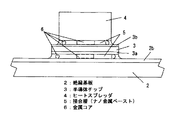
【解決手段】金属ナノ粒子,金属ナノ粒子の常温での凝集を抑制する有機分散材,加熱により有機分散材と反応する分散材捕捉材および前記分散材と分散材捕捉材との反応物質を捕捉して揮散させる揮発性有機成分を含む金属ペースト5を用いて半導体装置の絶縁基板2/半導体チップ3/ヒートスプレッダ4の部品間を導電,伝熱接合する接合方法において、接合部品の接合面域に前記の金属ペーストを塗布した状態で、接合層5の層厚に対応する線径の金属コア6を分散配置して重ね合わせた上で、続く加熱工程を経て部品間を接合する。これにより、金属コア6をスペーサとして部品間に前記揮発性有機成分の熱分解ガスを逃がす蒸散経路を確保して、接合層内に未接合部が生じるのを防止できる。
【選択図】図1
Description
ここで、前記のナノ金属ペーストを用いて金属部材(バルク材)の間を接合する場合に、従来の方法では一方の金属部材の接合面にナノ金属ペーストをスクリ−ン印刷法などにより塗布し、この上に相手側の金属部材を重ね合わせて軽い加圧力を加えた仮組立状態で、この仮組立体をリフロー炉に搬入して接合を行うようにしている。なお、加熱に伴う金属ナノ粒子間,および金属ナノ粒子と被接合金属部材との間の接合メカニズム,およびそのキュアー条件,接合強度,耐熱温度等の特性については、先記の非特許文献1および特許文献2に詳しく述べられており、加熱により活性化した金属ナノ粒子間,および金属ナノ粒子と金属粉,接合金属板との間で低温焼結による溶着/焼結(架橋)が進行し、最終的に抵抗率が低いマトリックス構造の接合層が形成される。
小田 正明,「ナノ金属粒子」,エレクトロニクス実装学会誌,2002年,vol5,No6,p523−528
前記の金属ペーストを被接合部品の接合面に塗布した状態で、部品の対向面間に金属コア材を分散介挿して重ね合わせ、続く加熱工程を経て接合するものとする(請求項1)。
また、本発明では、半導体装置の絶縁基板とその導体パターンに接合する半導体チップ、ないしは半導体チップとその上面に接合するヒートスプレッダを被接合部品として、前記した接合方法を適用して半導体装置を組み立てるようにする(請求項4)。
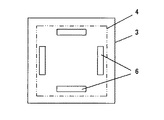
すなわち、図示実施例の半導体デバイスでは、絶縁基板2の導体パターン2bと半導体チップ3との間、および半導体チップ2とその上面側に積層したヒートスプレッダ4との間が先記したナノ金属ペーストを用いて接合されており、その接合層を符号5で、また後記のように被接合部品間の接合面域に分散介挿した金属コアを符号6で表している。
この加熱工程では、先述のように有機分散材と分散材捕捉材との反応により裸になって活性化した金属ナノ粒子同士,および金属ナノ粒子と金属粉,被接合部品との間で溶着,焼結(架橋)が進行し、最終的には絶縁基板2/半導体チップ3/ヒートスプレッダ4の部品相互間に、金属コア6の線径に対応する厚さでマトリックス構造の接合層5が形成される。しかも、この接合過程では前記金属コア6の介在によって部品相互間には周囲に通じる蒸散経路が確保されている。これにより、金属ナノ粒子の溶着,焼結が進行する過程で熱分解した有機成分は、特に接合面の中央面域においても被接合部品の間に封じ込められることなく、前記の蒸散経路を通じて周囲に蒸散するようになる。その結果として、接合層5には層中に未接合部分を残すことなく、接合面の全域で部品間を適正に接合することができて半導体デバイスの信頼性が向上する。
2b 導体パターン
3 半導体チップ
4 ヒートスプレッダ
5 接合層(ナノ金属ペースト)
6 金属コア
Claims (4)
- 金属ナノ粒子,金属ナノ粒子の常温での凝集を抑制する有機分散材,加熱により有機分散材と反応する分散材捕捉材および前記分散材と分散材捕捉材との反応物質を捕捉して揮散させる揮発性有機成分を含む金属ペーストを用いた半導体装置の部品間接合方法であって、表面が金属母材である被接合部品の接合面域に前記金属ペーストを塗布して被接合部品を重ね合わせた状態で加熱し、この加熱により金属ナノ粒子を低温焼結させて部品間を導電,伝熱接合するようにした接合方法において、
前記金属ペーストを被接合部品の接合面に塗布した状態で、部品の対向面間に金属コア材を分散介挿して重ね合わせ、続く加熱工程を経て接合することを特徴とする半導体装置の部品間接合方法。 - 請求項1に記載の接合方法において、金属ペーストの成分である金属ナノ粒子がAgナノ粒子,もしくはCuナノ粒子であることを特徴とする半導体装置の部品間接合方法。
- 請求項1に記載の接合方法において、金属コア材が、被接合部品間の接合層厚さに対応した線径の円柱状銅材であることを特徴とする半導体装置の部品間接合方法。
- 請求項1ないし3のいずれかの項に記載の接合方法において、金属ペーストを介して面接合される被接合部品が、絶縁基板とその導体パターンに接合する半導体チップ、ないしは半導体チップとその上面に接合するヒートスプレッダであることを特徴とする半導体装置の部品間接合方法。
Priority Applications (1)
| Application Number | Priority Date | Filing Date | Title |
|---|---|---|---|
| JP2006180770A JP2008010703A (ja) | 2006-06-30 | 2006-06-30 | 半導体装置の部品間接合方法 |
Applications Claiming Priority (1)
| Application Number | Priority Date | Filing Date | Title |
|---|---|---|---|
| JP2006180770A JP2008010703A (ja) | 2006-06-30 | 2006-06-30 | 半導体装置の部品間接合方法 |
Publications (1)
| Publication Number | Publication Date |
|---|---|
| JP2008010703A true JP2008010703A (ja) | 2008-01-17 |
Family
ID=39068632
Family Applications (1)
| Application Number | Title | Priority Date | Filing Date |
|---|---|---|---|
| JP2006180770A Withdrawn JP2008010703A (ja) | 2006-06-30 | 2006-06-30 | 半導体装置の部品間接合方法 |
Country Status (1)
| Country | Link |
|---|---|
| JP (1) | JP2008010703A (ja) |
Cited By (12)
| Publication number | Priority date | Publication date | Assignee | Title |
|---|---|---|---|---|
| WO2009094537A2 (en) * | 2008-01-24 | 2009-07-30 | Virginia Tech Intellectual Properties, Inc. | Nanoscale metal paste for interconnect and method of use |
| WO2009157160A1 (ja) * | 2008-06-25 | 2009-12-30 | パナソニック株式会社 | 実装構造体、及び実装構造体の製造方法 |
| EP2257142A1 (de) * | 2009-05-26 | 2010-12-01 | Semikron Elektronik GmbH & Co. KG Patentabteilung | Befestigung eines Bauelementes an einem Substrat und/oder eines Anschlusselementes an dem Bauelement oder an dem Substrat durch Drucksinterung |
| WO2010091660A3 (de) * | 2009-02-13 | 2011-06-03 | Danfoss Silicon Power Gmbh | Verfahren zur schaffung einer hochtemperatur- und temperaturwechselfesten verbindung eines baugruppen-halbleiters und eines halbleiterbausteins mit einem temperaturbeaufschlagenden verfahren |
| WO2013133085A1 (ja) * | 2012-03-05 | 2013-09-12 | ナミックス株式会社 | 銀微粒子焼結体 |
| JP2014517546A (ja) * | 2011-07-04 | 2014-07-17 | ローベルト ボツシユ ゲゼルシヤフト ミツト ベシユレンクテル ハフツング | 構造化された焼結結合層の製造方法及び構造化された焼結結合層を備えている半導体素子 |
| JP2014200824A (ja) * | 2013-04-05 | 2014-10-27 | 富士電機株式会社 | 静流体圧による加圧接合方法及びこれに使用する加圧接合装置 |
| WO2016146323A3 (de) * | 2015-03-16 | 2016-11-03 | Pac Tech - Packaging Technologies Gmbh | Chipanordnung und verfahren zur ausbildung einer kontaktverbindung |
| TWI629728B (zh) * | 2016-02-12 | 2018-07-11 | 國立大學法人大阪大學 | 接合材料及其製作方法與接合結構的製作方法 |
| WO2018155633A1 (ja) | 2017-02-23 | 2018-08-30 | 国立大学法人大阪大学 | 接合材、接合材の製造方法および接合構造体の作製方法 |
| JP2019508250A (ja) * | 2016-02-19 | 2019-03-28 | ヘラエウス ドイチュラント ゲゼルシャフト ミット ベシュレンクテル ハフツング ウント コンパニー コマンディトゲゼルシャフト | 熱拡散板の製造方法、熱拡散板、半導体モジュールの製造方法及び半導体モジュール |
| US10593851B2 (en) | 2017-04-28 | 2020-03-17 | Nichia Corporation | Metal powder sintering paste, method for producing the same, and method for producing conductive material |
-
2006
- 2006-06-30 JP JP2006180770A patent/JP2008010703A/ja not_active Withdrawn
Cited By (24)
| Publication number | Priority date | Publication date | Assignee | Title |
|---|---|---|---|---|
| US8257795B2 (en) | 2004-02-18 | 2012-09-04 | Virginia Tech Intellectual Properties, Inc. | Nanoscale metal paste for interconnect and method of use |
| WO2009094537A3 (en) * | 2008-01-24 | 2009-09-17 | Virginia Tech Intellectual Properties, Inc. | Nanoscale metal paste for interconnect and method of use |
| WO2009094537A2 (en) * | 2008-01-24 | 2009-07-30 | Virginia Tech Intellectual Properties, Inc. | Nanoscale metal paste for interconnect and method of use |
| EP2293324A1 (en) * | 2008-06-25 | 2011-03-09 | Panasonic Corporation | Packaging structure and method for manufacturing packaging structure |
| WO2009157160A1 (ja) * | 2008-06-25 | 2009-12-30 | パナソニック株式会社 | 実装構造体、及び実装構造体の製造方法 |
| CN102067298A (zh) * | 2008-06-25 | 2011-05-18 | 松下电器产业株式会社 | 安装结构体、以及安装结构体的制造方法 |
| JP5331113B2 (ja) * | 2008-06-25 | 2013-10-30 | パナソニック株式会社 | 実装構造体 |
| US9246073B2 (en) | 2008-06-25 | 2016-01-26 | Panasonic Intellectual Property Management Co., Ltd. | Mounting structure, and method of manufacturing mounting structure |
| EP2293324A4 (en) * | 2008-06-25 | 2014-09-10 | Panasonic Corp | PACKAGING STRUCTURE AND METHOD FOR MANUFACTURING PACKAGING STRUCTURE |
| WO2010091660A3 (de) * | 2009-02-13 | 2011-06-03 | Danfoss Silicon Power Gmbh | Verfahren zur schaffung einer hochtemperatur- und temperaturwechselfesten verbindung eines baugruppen-halbleiters und eines halbleiterbausteins mit einem temperaturbeaufschlagenden verfahren |
| US9287232B2 (en) | 2009-02-13 | 2016-03-15 | Danfoss Silicon Power Gmbh | Method for producing a high-temperature and temperature-change resistant connection between a semiconductor module and a connection partner |
| EP2257142A1 (de) * | 2009-05-26 | 2010-12-01 | Semikron Elektronik GmbH & Co. KG Patentabteilung | Befestigung eines Bauelementes an einem Substrat und/oder eines Anschlusselementes an dem Bauelement oder an dem Substrat durch Drucksinterung |
| JP2014517546A (ja) * | 2011-07-04 | 2014-07-17 | ローベルト ボツシユ ゲゼルシヤフト ミツト ベシユレンクテル ハフツング | 構造化された焼結結合層の製造方法及び構造化された焼結結合層を備えている半導体素子 |
| US9887173B2 (en) | 2011-07-04 | 2018-02-06 | Robert Bosch Gmbh | Method for producing structured sintered connection layers, and semiconductor element having a structured sintered connection layer |
| JPWO2013133085A1 (ja) * | 2012-03-05 | 2015-07-30 | ナミックス株式会社 | 銀微粒子焼結体 |
| WO2013133085A1 (ja) * | 2012-03-05 | 2013-09-12 | ナミックス株式会社 | 銀微粒子焼結体 |
| US10369667B2 (en) | 2012-03-05 | 2019-08-06 | Namics Corporation | Sintered body made from silver fine particles |
| JP2014200824A (ja) * | 2013-04-05 | 2014-10-27 | 富士電機株式会社 | 静流体圧による加圧接合方法及びこれに使用する加圧接合装置 |
| WO2016146323A3 (de) * | 2015-03-16 | 2016-11-03 | Pac Tech - Packaging Technologies Gmbh | Chipanordnung und verfahren zur ausbildung einer kontaktverbindung |
| TWI629728B (zh) * | 2016-02-12 | 2018-07-11 | 國立大學法人大阪大學 | 接合材料及其製作方法與接合結構的製作方法 |
| US11273525B2 (en) | 2016-02-12 | 2022-03-15 | Osaka University | Bonding material, method for producing bonding material, and method for producing bonding structure |
| JP2019508250A (ja) * | 2016-02-19 | 2019-03-28 | ヘラエウス ドイチュラント ゲゼルシャフト ミット ベシュレンクテル ハフツング ウント コンパニー コマンディトゲゼルシャフト | 熱拡散板の製造方法、熱拡散板、半導体モジュールの製造方法及び半導体モジュール |
| WO2018155633A1 (ja) | 2017-02-23 | 2018-08-30 | 国立大学法人大阪大学 | 接合材、接合材の製造方法および接合構造体の作製方法 |
| US10593851B2 (en) | 2017-04-28 | 2020-03-17 | Nichia Corporation | Metal powder sintering paste, method for producing the same, and method for producing conductive material |
Similar Documents
| Publication | Publication Date | Title |
|---|---|---|
| JP2008010703A (ja) | 半導体装置の部品間接合方法 | |
| JP4770379B2 (ja) | 金属部材の接合方法およびその組立治具 | |
| JP4904767B2 (ja) | 半導体装置 | |
| US11424170B2 (en) | Method for mounting an electrical component in which a hood is used, and a hood that is suitable for use in this method | |
| JP5705467B2 (ja) | 半導体装置の接合方法、および、半導体装置 | |
| JP2007044754A (ja) | 金属板接合方法 | |
| JP2012099779A (ja) | 焼成接合を用いたパワーモジュール及びその製造方法 | |
| JP4539980B2 (ja) | 半導体装置およびその製造方法 | |
| JP6206494B2 (ja) | 半導体装置 | |
| JP2007019360A (ja) | 電子部品の実装方法 | |
| US20150123263A1 (en) | Two-step method for joining a semiconductor to a substrate with connecting material based on silver | |
| JP5642336B2 (ja) | 半導体装置およびその製造方法 | |
| JP5659663B2 (ja) | 半導体装置及び半導体装置の製造方法 | |
| JP5252024B2 (ja) | 半導体装置 | |
| JP7215206B2 (ja) | 半導体装置の製造方法 | |
| JP5018250B2 (ja) | 半導体装置およびその製造方法 | |
| JP4877046B2 (ja) | 半導体装置およびその製造方法 | |
| JP6641524B1 (ja) | 半導体装置の製造方法 | |
| JP5560713B2 (ja) | 電子部品の実装方法等 | |
| JP2017005007A (ja) | 半導体装置、および半導体装置の製造方法 | |
| JP6019790B2 (ja) | 接合方法及び接合部材 | |
| JP2007266405A (ja) | Au−Sn合金はんだペーストを用いた基板と素子の接合方法 | |
| JP2008159849A (ja) | 電極接合構造体及び電極接合方法 | |
| JP6383208B2 (ja) | 半導体装置の製造方法、接合材および接合材の形成方法 | |
| JP6000227B2 (ja) | 半導体装置の製造方法 |
Legal Events
| Date | Code | Title | Description |
|---|---|---|---|
| A711 | Notification of change in applicant |
Free format text: JAPANESE INTERMEDIATE CODE: A711 Effective date: 20080204 |
|
| RD02 | Notification of acceptance of power of attorney |
Free format text: JAPANESE INTERMEDIATE CODE: A7422 Effective date: 20081216 |
|
| RD04 | Notification of resignation of power of attorney |
Free format text: JAPANESE INTERMEDIATE CODE: A7424 Effective date: 20090219 |
|
| A621 | Written request for application examination |
Free format text: JAPANESE INTERMEDIATE CODE: A621 Effective date: 20090323 |
|
| A711 | Notification of change in applicant |
Free format text: JAPANESE INTERMEDIATE CODE: A712 Effective date: 20091112 |
|
| A711 | Notification of change in applicant |
Free format text: JAPANESE INTERMEDIATE CODE: A712 Effective date: 20110422 |
|
| A977 | Report on retrieval |
Free format text: JAPANESE INTERMEDIATE CODE: A971007 Effective date: 20110621 |
|
| A131 | Notification of reasons for refusal |
Free format text: JAPANESE INTERMEDIATE CODE: A131 Effective date: 20110628 |
|
| A761 | Written withdrawal of application |
Free format text: JAPANESE INTERMEDIATE CODE: A761 Effective date: 20110829 |