JP2008010703A - Method for bonding between components of semiconductor device - Google Patents
Method for bonding between components of semiconductor device Download PDFInfo
- Publication number
- JP2008010703A JP2008010703A JP2006180770A JP2006180770A JP2008010703A JP 2008010703 A JP2008010703 A JP 2008010703A JP 2006180770 A JP2006180770 A JP 2006180770A JP 2006180770 A JP2006180770 A JP 2006180770A JP 2008010703 A JP2008010703 A JP 2008010703A
- Authority
- JP
- Japan
- Prior art keywords
- metal
- joining
- parts
- joined
- nanoparticles
- Prior art date
- Legal status (The legal status is an assumption and is not a legal conclusion. Google has not performed a legal analysis and makes no representation as to the accuracy of the status listed.)
- Withdrawn
Links
Images

Classifications
-
- H—ELECTRICITY
- H01—ELECTRIC ELEMENTS
- H01L—SEMICONDUCTOR DEVICES NOT COVERED BY CLASS H10
- H01L24/00—Arrangements for connecting or disconnecting semiconductor or solid-state bodies; Methods or apparatus related thereto
- H01L24/80—Methods for connecting semiconductor or other solid state bodies using means for bonding being attached to, or being formed on, the surface to be connected
- H01L24/83—Methods for connecting semiconductor or other solid state bodies using means for bonding being attached to, or being formed on, the surface to be connected using a layer connector
-
- H—ELECTRICITY
- H01—ELECTRIC ELEMENTS
- H01L—SEMICONDUCTOR DEVICES NOT COVERED BY CLASS H10
- H01L24/00—Arrangements for connecting or disconnecting semiconductor or solid-state bodies; Methods or apparatus related thereto
- H01L24/01—Means for bonding being attached to, or being formed on, the surface to be connected, e.g. chip-to-package, die-attach, "first-level" interconnects; Manufacturing methods related thereto
- H01L24/26—Layer connectors, e.g. plate connectors, solder or adhesive layers; Manufacturing methods related thereto
- H01L24/31—Structure, shape, material or disposition of the layer connectors after the connecting process
- H01L24/32—Structure, shape, material or disposition of the layer connectors after the connecting process of an individual layer connector
-
- H—ELECTRICITY
- H01—ELECTRIC ELEMENTS
- H01L—SEMICONDUCTOR DEVICES NOT COVERED BY CLASS H10
- H01L2224/00—Indexing scheme for arrangements for connecting or disconnecting semiconductor or solid-state bodies and methods related thereto as covered by H01L24/00
- H01L2224/01—Means for bonding being attached to, or being formed on, the surface to be connected, e.g. chip-to-package, die-attach, "first-level" interconnects; Manufacturing methods related thereto
- H01L2224/02—Bonding areas; Manufacturing methods related thereto
- H01L2224/04—Structure, shape, material or disposition of the bonding areas prior to the connecting process
- H01L2224/05—Structure, shape, material or disposition of the bonding areas prior to the connecting process of an individual bonding area
- H01L2224/0554—External layer
- H01L2224/05599—Material
- H01L2224/056—Material with a principal constituent of the material being a metal or a metalloid, e.g. boron [B], silicon [Si], germanium [Ge], arsenic [As], antimony [Sb], tellurium [Te] and polonium [Po], and alloys thereof
- H01L2224/05617—Material with a principal constituent of the material being a metal or a metalloid, e.g. boron [B], silicon [Si], germanium [Ge], arsenic [As], antimony [Sb], tellurium [Te] and polonium [Po], and alloys thereof the principal constituent melting at a temperature of greater than or equal to 400°C and less than 950°C
- H01L2224/05624—Aluminium [Al] as principal constituent
-
- H—ELECTRICITY
- H01—ELECTRIC ELEMENTS
- H01L—SEMICONDUCTOR DEVICES NOT COVERED BY CLASS H10
- H01L2224/00—Indexing scheme for arrangements for connecting or disconnecting semiconductor or solid-state bodies and methods related thereto as covered by H01L24/00
- H01L2224/01—Means for bonding being attached to, or being formed on, the surface to be connected, e.g. chip-to-package, die-attach, "first-level" interconnects; Manufacturing methods related thereto
- H01L2224/26—Layer connectors, e.g. plate connectors, solder or adhesive layers; Manufacturing methods related thereto
- H01L2224/28—Structure, shape, material or disposition of the layer connectors prior to the connecting process
- H01L2224/29—Structure, shape, material or disposition of the layer connectors prior to the connecting process of an individual layer connector
- H01L2224/29001—Core members of the layer connector
- H01L2224/29099—Material
- H01L2224/29198—Material with a principal constituent of the material being a combination of two or more materials in the form of a matrix with a filler, i.e. being a hybrid material, e.g. segmented structures, foams
- H01L2224/29298—Fillers
- H01L2224/29299—Base material
- H01L2224/293—Base material with a principal constituent of the material being a metal or a metalloid, e.g. boron [B], silicon [Si], germanium [Ge], arsenic [As], antimony [Sb], tellurium [Te] and polonium [Po], and alloys thereof
- H01L2224/29338—Base material with a principal constituent of the material being a metal or a metalloid, e.g. boron [B], silicon [Si], germanium [Ge], arsenic [As], antimony [Sb], tellurium [Te] and polonium [Po], and alloys thereof the principal constituent melting at a temperature of greater than or equal to 950°C and less than 1550°C
- H01L2224/29339—Silver [Ag] as principal constituent
-
- H—ELECTRICITY
- H01—ELECTRIC ELEMENTS
- H01L—SEMICONDUCTOR DEVICES NOT COVERED BY CLASS H10
- H01L2224/00—Indexing scheme for arrangements for connecting or disconnecting semiconductor or solid-state bodies and methods related thereto as covered by H01L24/00
- H01L2224/01—Means for bonding being attached to, or being formed on, the surface to be connected, e.g. chip-to-package, die-attach, "first-level" interconnects; Manufacturing methods related thereto
- H01L2224/26—Layer connectors, e.g. plate connectors, solder or adhesive layers; Manufacturing methods related thereto
- H01L2224/28—Structure, shape, material or disposition of the layer connectors prior to the connecting process
- H01L2224/29—Structure, shape, material or disposition of the layer connectors prior to the connecting process of an individual layer connector
- H01L2224/29001—Core members of the layer connector
- H01L2224/29099—Material
- H01L2224/29198—Material with a principal constituent of the material being a combination of two or more materials in the form of a matrix with a filler, i.e. being a hybrid material, e.g. segmented structures, foams
- H01L2224/29298—Fillers
- H01L2224/29299—Base material
- H01L2224/293—Base material with a principal constituent of the material being a metal or a metalloid, e.g. boron [B], silicon [Si], germanium [Ge], arsenic [As], antimony [Sb], tellurium [Te] and polonium [Po], and alloys thereof
- H01L2224/29338—Base material with a principal constituent of the material being a metal or a metalloid, e.g. boron [B], silicon [Si], germanium [Ge], arsenic [As], antimony [Sb], tellurium [Te] and polonium [Po], and alloys thereof the principal constituent melting at a temperature of greater than or equal to 950°C and less than 1550°C
- H01L2224/29347—Copper [Cu] as principal constituent
-
- H—ELECTRICITY
- H01—ELECTRIC ELEMENTS
- H01L—SEMICONDUCTOR DEVICES NOT COVERED BY CLASS H10
- H01L2224/00—Indexing scheme for arrangements for connecting or disconnecting semiconductor or solid-state bodies and methods related thereto as covered by H01L24/00
- H01L2224/01—Means for bonding being attached to, or being formed on, the surface to be connected, e.g. chip-to-package, die-attach, "first-level" interconnects; Manufacturing methods related thereto
- H01L2224/26—Layer connectors, e.g. plate connectors, solder or adhesive layers; Manufacturing methods related thereto
- H01L2224/31—Structure, shape, material or disposition of the layer connectors after the connecting process
- H01L2224/32—Structure, shape, material or disposition of the layer connectors after the connecting process of an individual layer connector
- H01L2224/321—Disposition
- H01L2224/32151—Disposition the layer connector connecting between a semiconductor or solid-state body and an item not being a semiconductor or solid-state body, e.g. chip-to-substrate, chip-to-passive
- H01L2224/32221—Disposition the layer connector connecting between a semiconductor or solid-state body and an item not being a semiconductor or solid-state body, e.g. chip-to-substrate, chip-to-passive the body and the item being stacked
- H01L2224/32225—Disposition the layer connector connecting between a semiconductor or solid-state body and an item not being a semiconductor or solid-state body, e.g. chip-to-substrate, chip-to-passive the body and the item being stacked the item being non-metallic, e.g. insulating substrate with or without metallisation
-
- H—ELECTRICITY
- H01—ELECTRIC ELEMENTS
- H01L—SEMICONDUCTOR DEVICES NOT COVERED BY CLASS H10
- H01L2224/00—Indexing scheme for arrangements for connecting or disconnecting semiconductor or solid-state bodies and methods related thereto as covered by H01L24/00
- H01L2224/01—Means for bonding being attached to, or being formed on, the surface to be connected, e.g. chip-to-package, die-attach, "first-level" interconnects; Manufacturing methods related thereto
- H01L2224/34—Strap connectors, e.g. copper straps for grounding power devices; Manufacturing methods related thereto
- H01L2224/36—Structure, shape, material or disposition of the strap connectors prior to the connecting process
- H01L2224/37—Structure, shape, material or disposition of the strap connectors prior to the connecting process of an individual strap connector
- H01L2224/37001—Core members of the connector
- H01L2224/37099—Material
- H01L2224/371—Material with a principal constituent of the material being a metal or a metalloid, e.g. boron [B], silicon [Si], germanium [Ge], arsenic [As], antimony [Sb], tellurium [Te] and polonium [Po], and alloys thereof
- H01L2224/37117—Material with a principal constituent of the material being a metal or a metalloid, e.g. boron [B], silicon [Si], germanium [Ge], arsenic [As], antimony [Sb], tellurium [Te] and polonium [Po], and alloys thereof the principal constituent melting at a temperature of greater than or equal to 400°C and less than 950°C
- H01L2224/37124—Aluminium [Al] as principal constituent
-
- H—ELECTRICITY
- H01—ELECTRIC ELEMENTS
- H01L—SEMICONDUCTOR DEVICES NOT COVERED BY CLASS H10
- H01L2224/00—Indexing scheme for arrangements for connecting or disconnecting semiconductor or solid-state bodies and methods related thereto as covered by H01L24/00
- H01L2224/01—Means for bonding being attached to, or being formed on, the surface to be connected, e.g. chip-to-package, die-attach, "first-level" interconnects; Manufacturing methods related thereto
- H01L2224/34—Strap connectors, e.g. copper straps for grounding power devices; Manufacturing methods related thereto
- H01L2224/36—Structure, shape, material or disposition of the strap connectors prior to the connecting process
- H01L2224/37—Structure, shape, material or disposition of the strap connectors prior to the connecting process of an individual strap connector
- H01L2224/37001—Core members of the connector
- H01L2224/37099—Material
- H01L2224/371—Material with a principal constituent of the material being a metal or a metalloid, e.g. boron [B], silicon [Si], germanium [Ge], arsenic [As], antimony [Sb], tellurium [Te] and polonium [Po], and alloys thereof
- H01L2224/37138—Material with a principal constituent of the material being a metal or a metalloid, e.g. boron [B], silicon [Si], germanium [Ge], arsenic [As], antimony [Sb], tellurium [Te] and polonium [Po], and alloys thereof the principal constituent melting at a temperature of greater than or equal to 950°C and less than 1550°C
- H01L2224/37147—Copper [Cu] as principal constituent
-
- H—ELECTRICITY
- H01—ELECTRIC ELEMENTS
- H01L—SEMICONDUCTOR DEVICES NOT COVERED BY CLASS H10
- H01L2224/00—Indexing scheme for arrangements for connecting or disconnecting semiconductor or solid-state bodies and methods related thereto as covered by H01L24/00
- H01L2224/01—Means for bonding being attached to, or being formed on, the surface to be connected, e.g. chip-to-package, die-attach, "first-level" interconnects; Manufacturing methods related thereto
- H01L2224/34—Strap connectors, e.g. copper straps for grounding power devices; Manufacturing methods related thereto
- H01L2224/39—Structure, shape, material or disposition of the strap connectors after the connecting process
- H01L2224/40—Structure, shape, material or disposition of the strap connectors after the connecting process of an individual strap connector
- H01L2224/4005—Shape
- H01L2224/4009—Loop shape
- H01L2224/40095—Kinked
-
- H—ELECTRICITY
- H01—ELECTRIC ELEMENTS
- H01L—SEMICONDUCTOR DEVICES NOT COVERED BY CLASS H10
- H01L2224/00—Indexing scheme for arrangements for connecting or disconnecting semiconductor or solid-state bodies and methods related thereto as covered by H01L24/00
- H01L2224/01—Means for bonding being attached to, or being formed on, the surface to be connected, e.g. chip-to-package, die-attach, "first-level" interconnects; Manufacturing methods related thereto
- H01L2224/34—Strap connectors, e.g. copper straps for grounding power devices; Manufacturing methods related thereto
- H01L2224/39—Structure, shape, material or disposition of the strap connectors after the connecting process
- H01L2224/40—Structure, shape, material or disposition of the strap connectors after the connecting process of an individual strap connector
- H01L2224/401—Disposition
- H01L2224/40151—Connecting between a semiconductor or solid-state body and an item not being a semiconductor or solid-state body, e.g. chip-to-substrate, chip-to-passive
- H01L2224/40221—Connecting between a semiconductor or solid-state body and an item not being a semiconductor or solid-state body, e.g. chip-to-substrate, chip-to-passive the body and the item being stacked
- H01L2224/40225—Connecting between a semiconductor or solid-state body and an item not being a semiconductor or solid-state body, e.g. chip-to-substrate, chip-to-passive the body and the item being stacked the item being non-metallic, e.g. insulating substrate with or without metallisation
-
- H—ELECTRICITY
- H01—ELECTRIC ELEMENTS
- H01L—SEMICONDUCTOR DEVICES NOT COVERED BY CLASS H10
- H01L2224/00—Indexing scheme for arrangements for connecting or disconnecting semiconductor or solid-state bodies and methods related thereto as covered by H01L24/00
- H01L2224/01—Means for bonding being attached to, or being formed on, the surface to be connected, e.g. chip-to-package, die-attach, "first-level" interconnects; Manufacturing methods related thereto
- H01L2224/34—Strap connectors, e.g. copper straps for grounding power devices; Manufacturing methods related thereto
- H01L2224/39—Structure, shape, material or disposition of the strap connectors after the connecting process
- H01L2224/40—Structure, shape, material or disposition of the strap connectors after the connecting process of an individual strap connector
- H01L2224/404—Connecting portions
- H01L2224/40475—Connecting portions connected to auxiliary connecting means on the bonding areas
- H01L2224/40491—Connecting portions connected to auxiliary connecting means on the bonding areas being an additional member attached to the bonding area through an adhesive or solder, e.g. buffer pad
-
- H—ELECTRICITY
- H01—ELECTRIC ELEMENTS
- H01L—SEMICONDUCTOR DEVICES NOT COVERED BY CLASS H10
- H01L2224/00—Indexing scheme for arrangements for connecting or disconnecting semiconductor or solid-state bodies and methods related thereto as covered by H01L24/00
- H01L2224/73—Means for bonding being of different types provided for in two or more of groups H01L2224/10, H01L2224/18, H01L2224/26, H01L2224/34, H01L2224/42, H01L2224/50, H01L2224/63, H01L2224/71
- H01L2224/732—Location after the connecting process
- H01L2224/73251—Location after the connecting process on different surfaces
- H01L2224/73263—Layer and strap connectors
-
- H—ELECTRICITY
- H01—ELECTRIC ELEMENTS
- H01L—SEMICONDUCTOR DEVICES NOT COVERED BY CLASS H10
- H01L2224/00—Indexing scheme for arrangements for connecting or disconnecting semiconductor or solid-state bodies and methods related thereto as covered by H01L24/00
- H01L2224/74—Apparatus for manufacturing arrangements for connecting or disconnecting semiconductor or solid-state bodies and for methods related thereto
- H01L2224/75—Apparatus for connecting with bump connectors or layer connectors
- H01L2224/7525—Means for applying energy, e.g. heating means
- H01L2224/75272—Oven
-
- H—ELECTRICITY
- H01—ELECTRIC ELEMENTS
- H01L—SEMICONDUCTOR DEVICES NOT COVERED BY CLASS H10
- H01L2224/00—Indexing scheme for arrangements for connecting or disconnecting semiconductor or solid-state bodies and methods related thereto as covered by H01L24/00
- H01L2224/74—Apparatus for manufacturing arrangements for connecting or disconnecting semiconductor or solid-state bodies and for methods related thereto
- H01L2224/77—Apparatus for connecting with strap connectors
- H01L2224/7725—Means for applying energy, e.g. heating means
- H01L2224/77272—Oven
-
- H—ELECTRICITY
- H01—ELECTRIC ELEMENTS
- H01L—SEMICONDUCTOR DEVICES NOT COVERED BY CLASS H10
- H01L2224/00—Indexing scheme for arrangements for connecting or disconnecting semiconductor or solid-state bodies and methods related thereto as covered by H01L24/00
- H01L2224/80—Methods for connecting semiconductor or other solid state bodies using means for bonding being attached to, or being formed on, the surface to be connected
- H01L2224/83—Methods for connecting semiconductor or other solid state bodies using means for bonding being attached to, or being formed on, the surface to be connected using a layer connector
- H01L2224/8312—Aligning
- H01L2224/83136—Aligning involving guiding structures, e.g. spacers or supporting members
- H01L2224/83138—Aligning involving guiding structures, e.g. spacers or supporting members the guiding structures being at least partially left in the finished device
- H01L2224/8314—Guiding structures outside the body
-
- H—ELECTRICITY
- H01—ELECTRIC ELEMENTS
- H01L—SEMICONDUCTOR DEVICES NOT COVERED BY CLASS H10
- H01L2224/00—Indexing scheme for arrangements for connecting or disconnecting semiconductor or solid-state bodies and methods related thereto as covered by H01L24/00
- H01L2224/80—Methods for connecting semiconductor or other solid state bodies using means for bonding being attached to, or being formed on, the surface to be connected
- H01L2224/83—Methods for connecting semiconductor or other solid state bodies using means for bonding being attached to, or being formed on, the surface to be connected using a layer connector
- H01L2224/8338—Bonding interfaces outside the semiconductor or solid-state body
- H01L2224/83399—Material
- H01L2224/834—Material with a principal constituent of the material being a metal or a metalloid, e.g. boron [B], silicon [Si], germanium [Ge], arsenic [As], antimony [Sb], tellurium [Te] and polonium [Po], and alloys thereof
- H01L2224/83438—Material with a principal constituent of the material being a metal or a metalloid, e.g. boron [B], silicon [Si], germanium [Ge], arsenic [As], antimony [Sb], tellurium [Te] and polonium [Po], and alloys thereof the principal constituent melting at a temperature of greater than or equal to 950°C and less than 1550°C
- H01L2224/83447—Copper [Cu] as principal constituent
-
- H—ELECTRICITY
- H01—ELECTRIC ELEMENTS
- H01L—SEMICONDUCTOR DEVICES NOT COVERED BY CLASS H10
- H01L2224/00—Indexing scheme for arrangements for connecting or disconnecting semiconductor or solid-state bodies and methods related thereto as covered by H01L24/00
- H01L2224/80—Methods for connecting semiconductor or other solid state bodies using means for bonding being attached to, or being formed on, the surface to be connected
- H01L2224/83—Methods for connecting semiconductor or other solid state bodies using means for bonding being attached to, or being formed on, the surface to be connected using a layer connector
- H01L2224/838—Bonding techniques
- H01L2224/83801—Soldering or alloying
-
- H—ELECTRICITY
- H01—ELECTRIC ELEMENTS
- H01L—SEMICONDUCTOR DEVICES NOT COVERED BY CLASS H10
- H01L2224/00—Indexing scheme for arrangements for connecting or disconnecting semiconductor or solid-state bodies and methods related thereto as covered by H01L24/00
- H01L2224/80—Methods for connecting semiconductor or other solid state bodies using means for bonding being attached to, or being formed on, the surface to be connected
- H01L2224/83—Methods for connecting semiconductor or other solid state bodies using means for bonding being attached to, or being formed on, the surface to be connected using a layer connector
- H01L2224/838—Bonding techniques
- H01L2224/8384—Sintering
-
- H—ELECTRICITY
- H01—ELECTRIC ELEMENTS
- H01L—SEMICONDUCTOR DEVICES NOT COVERED BY CLASS H10
- H01L2224/00—Indexing scheme for arrangements for connecting or disconnecting semiconductor or solid-state bodies and methods related thereto as covered by H01L24/00
- H01L2224/80—Methods for connecting semiconductor or other solid state bodies using means for bonding being attached to, or being formed on, the surface to be connected
- H01L2224/84—Methods for connecting semiconductor or other solid state bodies using means for bonding being attached to, or being formed on, the surface to be connected using a strap connector
- H01L2224/8412—Aligning
- H01L2224/84136—Aligning involving guiding structures, e.g. spacers or supporting members
- H01L2224/84138—Aligning involving guiding structures, e.g. spacers or supporting members the guiding structures being at least partially left in the finished device
-
- H—ELECTRICITY
- H01—ELECTRIC ELEMENTS
- H01L—SEMICONDUCTOR DEVICES NOT COVERED BY CLASS H10
- H01L2224/00—Indexing scheme for arrangements for connecting or disconnecting semiconductor or solid-state bodies and methods related thereto as covered by H01L24/00
- H01L2224/80—Methods for connecting semiconductor or other solid state bodies using means for bonding being attached to, or being formed on, the surface to be connected
- H01L2224/84—Methods for connecting semiconductor or other solid state bodies using means for bonding being attached to, or being formed on, the surface to be connected using a strap connector
- H01L2224/8438—Bonding interfaces outside the semiconductor or solid-state body
- H01L2224/84399—Material
- H01L2224/844—Material with a principal constituent of the material being a metal or a metalloid, e.g. boron [B], silicon [Si], germanium [Ge], arsenic [As], antimony [Sb], tellurium [Te] and polonium [Po], and alloys thereof
- H01L2224/84438—Material with a principal constituent of the material being a metal or a metalloid, e.g. boron [B], silicon [Si], germanium [Ge], arsenic [As], antimony [Sb], tellurium [Te] and polonium [Po], and alloys thereof the principal constituent melting at a temperature of greater than or equal to 950°C and less than 1550°C
- H01L2224/84447—Copper [Cu] as principal constituent
-
- H—ELECTRICITY
- H01—ELECTRIC ELEMENTS
- H01L—SEMICONDUCTOR DEVICES NOT COVERED BY CLASS H10
- H01L2224/00—Indexing scheme for arrangements for connecting or disconnecting semiconductor or solid-state bodies and methods related thereto as covered by H01L24/00
- H01L2224/80—Methods for connecting semiconductor or other solid state bodies using means for bonding being attached to, or being formed on, the surface to be connected
- H01L2224/84—Methods for connecting semiconductor or other solid state bodies using means for bonding being attached to, or being formed on, the surface to be connected using a strap connector
- H01L2224/848—Bonding techniques
- H01L2224/84801—Soldering or alloying
-
- H—ELECTRICITY
- H01—ELECTRIC ELEMENTS
- H01L—SEMICONDUCTOR DEVICES NOT COVERED BY CLASS H10
- H01L2224/00—Indexing scheme for arrangements for connecting or disconnecting semiconductor or solid-state bodies and methods related thereto as covered by H01L24/00
- H01L2224/80—Methods for connecting semiconductor or other solid state bodies using means for bonding being attached to, or being formed on, the surface to be connected
- H01L2224/84—Methods for connecting semiconductor or other solid state bodies using means for bonding being attached to, or being formed on, the surface to be connected using a strap connector
- H01L2224/848—Bonding techniques
- H01L2224/8484—Sintering
-
- H—ELECTRICITY
- H01—ELECTRIC ELEMENTS
- H01L—SEMICONDUCTOR DEVICES NOT COVERED BY CLASS H10
- H01L2224/00—Indexing scheme for arrangements for connecting or disconnecting semiconductor or solid-state bodies and methods related thereto as covered by H01L24/00
- H01L2224/80—Methods for connecting semiconductor or other solid state bodies using means for bonding being attached to, or being formed on, the surface to be connected
- H01L2224/84—Methods for connecting semiconductor or other solid state bodies using means for bonding being attached to, or being formed on, the surface to be connected using a strap connector
- H01L2224/848—Bonding techniques
- H01L2224/8485—Bonding techniques using a polymer adhesive, e.g. an adhesive based on silicone, epoxy, polyimide, polyester
-
- H—ELECTRICITY
- H01—ELECTRIC ELEMENTS
- H01L—SEMICONDUCTOR DEVICES NOT COVERED BY CLASS H10
- H01L2224/00—Indexing scheme for arrangements for connecting or disconnecting semiconductor or solid-state bodies and methods related thereto as covered by H01L24/00
- H01L2224/91—Methods for connecting semiconductor or solid state bodies including different methods provided for in two or more of groups H01L2224/80 - H01L2224/90
- H01L2224/92—Specific sequence of method steps
- H01L2224/922—Connecting different surfaces of the semiconductor or solid-state body with connectors of different types
- H01L2224/9221—Parallel connecting processes
-
- H—ELECTRICITY
- H01—ELECTRIC ELEMENTS
- H01L—SEMICONDUCTOR DEVICES NOT COVERED BY CLASS H10
- H01L24/00—Arrangements for connecting or disconnecting semiconductor or solid-state bodies; Methods or apparatus related thereto
- H01L24/01—Means for bonding being attached to, or being formed on, the surface to be connected, e.g. chip-to-package, die-attach, "first-level" interconnects; Manufacturing methods related thereto
- H01L24/02—Bonding areas ; Manufacturing methods related thereto
- H01L24/04—Structure, shape, material or disposition of the bonding areas prior to the connecting process
- H01L24/05—Structure, shape, material or disposition of the bonding areas prior to the connecting process of an individual bonding area
-
- H—ELECTRICITY
- H01—ELECTRIC ELEMENTS
- H01L—SEMICONDUCTOR DEVICES NOT COVERED BY CLASS H10
- H01L24/00—Arrangements for connecting or disconnecting semiconductor or solid-state bodies; Methods or apparatus related thereto
- H01L24/01—Means for bonding being attached to, or being formed on, the surface to be connected, e.g. chip-to-package, die-attach, "first-level" interconnects; Manufacturing methods related thereto
- H01L24/26—Layer connectors, e.g. plate connectors, solder or adhesive layers; Manufacturing methods related thereto
- H01L24/28—Structure, shape, material or disposition of the layer connectors prior to the connecting process
- H01L24/29—Structure, shape, material or disposition of the layer connectors prior to the connecting process of an individual layer connector
-
- H—ELECTRICITY
- H01—ELECTRIC ELEMENTS
- H01L—SEMICONDUCTOR DEVICES NOT COVERED BY CLASS H10
- H01L24/00—Arrangements for connecting or disconnecting semiconductor or solid-state bodies; Methods or apparatus related thereto
- H01L24/73—Means for bonding being of different types provided for in two or more of groups H01L24/10, H01L24/18, H01L24/26, H01L24/34, H01L24/42, H01L24/50, H01L24/63, H01L24/71
-
- H—ELECTRICITY
- H01—ELECTRIC ELEMENTS
- H01L—SEMICONDUCTOR DEVICES NOT COVERED BY CLASS H10
- H01L2924/00—Indexing scheme for arrangements or methods for connecting or disconnecting semiconductor or solid-state bodies as covered by H01L24/00
- H01L2924/013—Alloys
- H01L2924/0132—Binary Alloys
- H01L2924/01322—Eutectic Alloys, i.e. obtained by a liquid transforming into two solid phases
-
- H—ELECTRICITY
- H01—ELECTRIC ELEMENTS
- H01L—SEMICONDUCTOR DEVICES NOT COVERED BY CLASS H10
- H01L2924/00—Indexing scheme for arrangements or methods for connecting or disconnecting semiconductor or solid-state bodies as covered by H01L24/00
- H01L2924/013—Alloys
- H01L2924/0132—Binary Alloys
- H01L2924/01327—Intermediate phases, i.e. intermetallics compounds
-
- H—ELECTRICITY
- H01—ELECTRIC ELEMENTS
- H01L—SEMICONDUCTOR DEVICES NOT COVERED BY CLASS H10
- H01L2924/00—Indexing scheme for arrangements or methods for connecting or disconnecting semiconductor or solid-state bodies as covered by H01L24/00
- H01L2924/013—Alloys
- H01L2924/014—Solder alloys
-
- H—ELECTRICITY
- H01—ELECTRIC ELEMENTS
- H01L—SEMICONDUCTOR DEVICES NOT COVERED BY CLASS H10
- H01L2924/00—Indexing scheme for arrangements or methods for connecting or disconnecting semiconductor or solid-state bodies as covered by H01L24/00
- H01L2924/10—Details of semiconductor or other solid state devices to be connected
- H01L2924/11—Device type
- H01L2924/13—Discrete devices, e.g. 3 terminal devices
- H01L2924/1304—Transistor
- H01L2924/1305—Bipolar Junction Transistor [BJT]
- H01L2924/13055—Insulated gate bipolar transistor [IGBT]
Abstract
Description
本発明は、パワー半導体デバイスなどを対象に、その絶縁基板の導体パターンと半導体チップとの間、および半導体チップとその上面に積層したヒートスプレッダとの間を、金属ナノ粒子を含む金属ペーストを用いて接合する半導体装置の部品間接合方法に関する。 The present invention uses a metal paste containing metal nanoparticles between a conductive pattern of an insulating substrate and a semiconductor chip, and between a semiconductor chip and a heat spreader laminated on the upper surface thereof for a power semiconductor device or the like. The present invention relates to a method for joining parts of semiconductor devices to be joined.
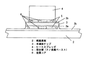
まず、本発明の実施対象となる頭記のパワー半導体デバイスについて、従来例の組立構造を図3に示す。図において、1は放熱用銅ベース、2はアルミナなどのセラミック板2aの上下両面に導体パターン(銅箔)2b,2cを形成して前記銅ベース1の上に搭載して接合した絶縁基板(例えば、Direct Bonding Copper基板)、3は絶縁基板2の上面導体パターン(回路パターン)2cにマウントした半導体チップ(例えば、IGBT)、3aは半導体チップ3の下面電極面にメタライズしたNi/Auメッキ膜、3bはチップ上面にメタライズしたアルミ膜、4は半導体チップ3の上面に接合したヒートスプレッダ(例えば、特許文献1参照)、5はヒートスプレッダ4を介して半導体チップ3の上面電極とこれに対応する導体パターン2cとの間に配線したリードフレーム(銅,アルミ材の導体)、6は導体パターン2cに接合した外部導出リードであり、銅ベース1/絶縁基板2の導体パターン2b,絶縁基板2の導体パターン2c/半導体チップ3,半導体チップ3の上面/ヒートスプレッダ4,ヒートスプレッダ4/リードフレーム5,絶縁基板2の導体パターン2c/リード5,6の間をそれぞれ半田7により接合してモジュールを組立てている。
First, an assembly structure of a conventional example is shown in FIG. 3 for the power semiconductor device described above which is an object of the present invention. In the figure, 1 is a heat-dissipating copper base, 2 is an insulating substrate (2) formed with conductive patterns (copper foils) 2b and 2c on the upper and lower surfaces of a
ところで、前記した半導体デバイスの各部品間を接合する半田について、昨今では環境保全の問題からSn−Pb系の共晶半田を鉛フリー半田(例えばSn−Ag系半田)に代替する転換が進められている。しかしながら、鉛フリー半田はSn−Pb半田に比べて融点が高く、また熱履歴により接合界面に生成する金属間化合物により半田接合部への応力集中が大きくなり、さらに過電流により半導体チップに半田の融点を超える熱が発生した場合には半田接合部に溶融,剥離,短絡などのダメージが発生するおそれがあるなど、このことが原因で半導体モジュールのパワーサイクル耐性,信頼性低下が大きな問題となっている。 By the way, with regard to the solder for joining the respective components of the semiconductor device described above, recently, a change in which Sn-Pb eutectic solder is replaced with lead-free solder (for example, Sn-Ag solder) has been promoted due to environmental conservation problems. ing. However, lead-free solder has a higher melting point than Sn-Pb solder, and stress concentration at the solder joint becomes large due to the intermetallic compound generated at the joint interface due to thermal history, and further, overcurrent causes solder to be applied to the semiconductor chip. If heat exceeding the melting point is generated, damage such as melting, peeling, or short-circuiting may occur at the solder joints. This causes major problems such as power cycle resistance and reduced reliability of the semiconductor module. ing.
一方、最近になり金属ナノ粒子の研究が進み、半導体デバイスの製造技術分野でも金属ナノ粒子の量子サイズ効果による低温焼結現象および高い表面活性を利用した低温焼成形の導電性ペースト(以下「ナノ金属ペースト」と称する)が開発されている(例えば、非特許文献1参照)。このナノ金属ペーストは、AgあるいはCuなどの金属ナノ粒子と、金属ナノ粒子が常温で凝集するのを抑制してナノ粒子を独立分散状態に保持する有機分散材と、加熱により有機分散材と反応して金属ナノ粒子を裸にする分散材捕捉材,および前記分散材と分散材捕捉材との反応物質を捕捉してガス化する揮発性有機成分(溶剤)を金属粉(骨材)と混練してペースト化したものである。 On the other hand, recently, research on metal nanoparticles has progressed, and in the field of semiconductor device manufacturing technology, a low-temperature sintered conductive paste (hereinafter referred to as “nano” (Referred to as non-patent document 1). This nanometal paste includes metal nanoparticles such as Ag or Cu, an organic dispersion material that keeps the nanoparticles from aggregating at room temperature and keeping the nanoparticles in an independent dispersion state, and reacts with the organic dispersion material by heating. Kneaded with metal powder (aggregate), a dispersion trapping material that bares metal nanoparticles, and a volatile organic component (solvent) that traps and gasifies the reactants of the dispersion material and the dispersion trapping material. And made into a paste.
さらに在来の半田接合の代わりに金属ナノ粒子を含む金属ペーストを用いて半導体デバイスの部品間を接合するようにしたものも知られている(例えば、特許文献2,特許文献3参照)。
ここで、前記のナノ金属ペーストを用いて金属部材(バルク材)の間を接合する場合に、従来の方法では一方の金属部材の接合面にナノ金属ペーストをスクリ−ン印刷法などにより塗布し、この上に相手側の金属部材を重ね合わせて軽い加圧力を加えた仮組立状態で、この仮組立体をリフロー炉に搬入して接合を行うようにしている。なお、加熱に伴う金属ナノ粒子間,および金属ナノ粒子と被接合金属部材との間の接合メカニズム,およびそのキュアー条件,接合強度,耐熱温度等の特性については、先記の非特許文献1および特許文献2に詳しく述べられており、加熱により活性化した金属ナノ粒子間,および金属ナノ粒子と金属粉,接合金属板との間で低温焼結による溶着/焼結(架橋)が進行し、最終的に抵抗率が低いマトリックス構造の接合層が形成される。
Further, there is also known one in which parts of semiconductor devices are joined using a metal paste containing metal nanoparticles instead of conventional solder joining (see, for example,
Here, when joining between metal members (bulk materials) using the nano metal paste, the nano metal paste is applied to the joining surface of one metal member by a screen printing method or the like in the conventional method. In addition, in a temporary assembly state in which a metal member on the other side is superposed on this and a light pressurizing force is applied, the temporary assembly is carried into a reflow furnace for bonding. In addition, about the joining mechanism between metal nanoparticles accompanying heating, and between metal nanoparticles and a to-be-joined metal member, and its characteristics, such as a curing condition, joining strength, and heat-resistant temperature, the above-mentioned
上記のように半導体デバイスの部品間接合法として、在来の半田接合に代えてナノ金属ペーストを用いて接合することにより、低い抵抗率と高い耐熱性,伝熱性,接合強度が得られ、またナノ金属粒子(銀,銅)の溶融温度以下では接合部が溶断することもないなど、半田接合に較べて高信頼性の接合が期待できる。
ところで、図3に示した半導体デバイスの部品接合について、発明者等がナノ金属ペーストを適用した場合の接合条件などに関して様々な実験,検証を行ったところ、従来のリフロー半田付けと同様な手法で部品の接合面に塗布したナノ金属ペーストに接合相手の部品を重ね合わせた上で軽く加圧力を加えて仮組み立てし、この仮組立状態でリフロー炉に搬入して接合を行った場合には接合面の中央部分に未接合の欠陥が多く発生することが知見された。 By the way, when the inventors conducted various experiments and verifications regarding the bonding conditions of the semiconductor device shown in FIG. 3 regarding the bonding conditions when the nano metal paste is applied, the same method as in conventional reflow soldering is used. When the parts to be joined are superimposed on the nano metal paste applied to the joining surface of the parts, light pressure is applied to temporarily assemble, and when the parts are brought into the reflow furnace and joined in this temporarily assembled state, they are joined. It was found that many unbonded defects occur in the central part of the surface.
そこで、発明者等はこの接合欠陥の発生原因について究明した結果、その発生要因が次の点にあることが明らかになった。すなわち、金属ナノ粒子の粒子間,および金属ナノ粒子と被接合金属部材(図3における絶縁基板の導体パターン,半導体チップ,ヒートスプレッダ)との間で融着/焼結を適正に進めるには、金属ナノ粒子を独立分散状態に保持している分散材と分散材捕捉材との反応促進に加えて、この反応物質を捕捉した揮発性物質を蒸散させて接合面域から排除し、金属ナノ粒子を裸の状態にしてその表面活性を高めるようにすることが必須条件となる。 Thus, as a result of investigating the cause of the occurrence of this bonding defect, the inventors have found that the cause of the occurrence is as follows. That is, in order to properly promote the fusion / sintering between the metal nanoparticles and between the metal nanoparticles and the metal member to be joined (conductor pattern of the insulating substrate, semiconductor chip, heat spreader in FIG. 3) In addition to facilitating the reaction between the dispersion material holding the nanoparticles in an independently dispersed state and the dispersion material trapping material, the volatile material that traps the reaction material is evaporated to remove it from the joint area, and the metal nanoparticles are removed. It is essential to increase the surface activity in a naked state.
しかしながら、接合面に塗布したナノ金属ペーストを挟んで両側から半導体チップ3,絶縁基板2,ヒートスプレッダ4などの被接合部品を重ねて加圧力を加えた状態で加熱すると、特に接合面の中央面域におけるナノ金属ペーストが部品の間に封じ込められているために、加熱分解した有機成分の周囲への自由な蒸散(脱ガス)が阻害されることになる。このために接合面の中央面域では金属ナノ粒子の融着/焼結が十分に進行せず、結果として接合部に未接合部分が残るようになるものと推測される。
However, when heating is performed in a state where pressure is applied by overlapping parts to be joined such as the
本発明は上記の点に鑑みなされたものであり、図3のように半導体チップの両主面に絶縁基板,ヒートスプレッダなどの部品を重ねてその相互間を面接合した半導体デバイスなどを対象に、ナノ金属ペーストを用いて部品間を接合させる際に、接合層内に未接合部分を残すことなく接合面全域で適正に接合できるように改良した半導体装置の部品間接合方法を提供することを目的とする。 The present invention has been made in view of the above points, and is intended for a semiconductor device in which components such as an insulating substrate and a heat spreader are overlapped on both main surfaces of a semiconductor chip as shown in FIG. An object of the present invention is to provide an improved method for joining parts of a semiconductor device so that when joining parts using a nano metal paste, the joining layer can be properly joined over the entire joining surface without leaving an unjoined part in the joining layer. And
上記目的を達成するために、本発明によれば、金属ナノ粒子,金属ナノ粒子の常温での凝集を抑制する有機分散材,加熱により有機分散材と反応する分散材捕捉材および前記分散材と分散材捕捉材との反応物質を捕捉して揮散させる揮発性有機成分を含む金属ペーストを用いた半導体装置の部品間接合方法であって、表面が金属母材である被接合部品の接合面域に前記金属ペーストを塗布して被接合部品を重ね合わせた状態で加熱し、この加熱により金属ナノ粒子を低温焼結させて部品間を導電,伝熱接合するようにした接合方法において、
前記の金属ペーストを被接合部品の接合面に塗布した状態で、部品の対向面間に金属コア材を分散介挿して重ね合わせ、続く加熱工程を経て接合するものとする(請求項1)。
In order to achieve the above object, according to the present invention, metal nanoparticles, an organic dispersion that suppresses aggregation of metal nanoparticles at room temperature, a dispersion capturing material that reacts with an organic dispersion by heating, and the dispersion A method for joining parts of a semiconductor device using a metal paste containing a volatile organic component that captures and volatilizes a reactant with a dispersion material trapping material, the surface of which a surface is a metal base material, and is a joint surface area of a part to be joined In the joining method in which the metal paste is applied and heated in a state in which the parts to be joined are overlapped, and the metal nanoparticles are sintered at a low temperature by this heating to conduct conduction and heat transfer between the parts.
In a state where the metal paste is applied to the joining surface of the parts to be joined, the metal core material is dispersed and superimposed between the opposing faces of the parts, and joined through a subsequent heating process.
ここで、前記の金属ペーストに含まれる金属ナノ粒子は、Agナノ粒子もしくはCuナノ粒子であり(請求項2)、また金属コア材は、被接合部品間の接合層厚さに対応した線径の円柱状銅材である(請求項3)。
また、本発明では、半導体装置の絶縁基板とその導体パターンに接合する半導体チップ、ないしは半導体チップとその上面に接合するヒートスプレッダを被接合部品として、前記した接合方法を適用して半導体装置を組み立てるようにする(請求項4)。
Here, the metal nanoparticles contained in the metal paste are Ag nanoparticles or Cu nanoparticles (Claim 2), and the metal core material has a wire diameter corresponding to the joining layer thickness between the parts to be joined. (Claim 3).
Further, in the present invention, the semiconductor device is assembled by applying the above-described bonding method using the semiconductor substrate bonded to the insulating substrate of the semiconductor device and the conductor pattern, or the semiconductor chip and the heat spreader bonded to the upper surface thereof as the components to be bonded. (Claim 4).
上記接合方法のように、被接合部品の接合面にナノ金属ペーストを塗布し、さらにその塗布面に金属コア材を分散配置した上で部品を重ねて加圧した仮組立状態では、金属コア材をスペーサとして部品相互間に間隔が保持され、続く加熱工程で加熱分解する揮発性有機成分の周囲への蒸散経路が確保されることになる。なお、金属ナノ粒子を低温焼結させる金属ペーストのキュア条件は200℃前後であることから、加熱工程で金属コア材(銅材)が溶融することはない。 In the temporary assembly state in which the nano metal paste is applied to the joining surface of the parts to be joined and the metal core material is dispersed and arranged on the application surface and the parts are stacked and pressed as in the above joining method, the metal core material As a spacer, a space is maintained between the components, and a transpiration path to the periphery of the volatile organic component that is thermally decomposed in the subsequent heating process is secured. In addition, since the curing condition of the metal paste for sintering the metal nanoparticles at low temperature is around 200 ° C., the metal core material (copper material) is not melted in the heating process.
したがって、加熱による接合反応の進行に伴って加熱分解するナノ金属ペーストの揮発性有機成分は部品の間に封じ込められたままになることなく、前記金属コアの介挿により確保された蒸散経路を通じて周囲に蒸散する。これにより、接合面に塗布したナノ金属ペーストの全域で金属ナノ粒子の分散材と分散材捕捉材との反応促進,およびその熱分解ガスの蒸散が被接合部品に阻害されることなく進行し。その結果として金属ナノ粒子の表面活性が高まり、接合面全域で未接合(欠陥)のない部品間の接合が達成される。 Therefore, the volatile organic component of the nano metal paste that decomposes by heating as the joining reaction proceeds by heating does not remain confined between the parts, but through the transpiration path secured by the insertion of the metal core. Transpiration. As a result, the reaction between the metal nanoparticle dispersion material and the dispersion material trapping material is promoted over the entire area of the nanometal paste applied to the joining surface, and the evaporation of the pyrolysis gas proceeds without being obstructed by the parts to be joined. As a result, the surface activity of the metal nanoparticles is increased, and bonding between parts without unbonding (defects) is achieved over the entire bonding surface.
しかも、前記の金属コア材として、接合層厚に対応した線径の円柱状銅材を用いたことにより、被接合部品を重ね合わせる仮組立の過程でコア材が転がったり動いたりして介挿位置が多少変位しても部品相互間の間隔,平行度を安定保持できる。 In addition, by using a cylindrical copper material having a wire diameter corresponding to the thickness of the joining layer as the metal core material, the core material rolls or moves in the process of temporary assembly for overlapping the parts to be joined. Even if the position is slightly displaced, the distance between parts and parallelism can be maintained stably.
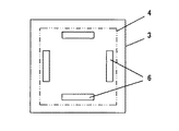
以下、本発明の実施の形態を図1,図2に示す実施例に基づいて説明する。なお、図1は本発明の接合方法を適用して組立てた半導体デバイスの組立構造図、図2は被接合部品の接合面域に分散配置した金属コアを表した模式図であり、図中で図3に対応する部材には同じ符号を付してその説明は省略する。
すなわち、図示実施例の半導体デバイスでは、絶縁基板2の導体パターン2bと半導体チップ3との間、および半導体チップ2とその上面側に積層したヒートスプレッダ4との間が先記したナノ金属ペーストを用いて接合されており、その接合層を符号5で、また後記のように被接合部品間の接合面域に分散介挿した金属コアを符号6で表している。
DESCRIPTION OF THE PREFERRED EMBODIMENTS Embodiments of the present invention will be described below based on the examples shown in FIGS. FIG. 1 is an assembly structure diagram of a semiconductor device assembled by applying the joining method of the present invention, and FIG. 2 is a schematic diagram showing metal cores distributed and arranged in the joining surface area of the parts to be joined. The members corresponding to those in FIG. 3 are denoted by the same reference numerals, and the description thereof is omitted.
That is, in the semiconductor device of the illustrated embodiment, the nano metal paste described above is used between the
ここで、図示の半導体チップ3は、例えば一辺の長さが7.5mm角のIGBTチップである。また、ナノ金属ペーストとしては、Agナノ粒子,あるいはCuナノ粒子を主要成分として、これに有機分散材,分散材捕捉材,揮発性有機成分(溶剤),および銀粉,銅粉などの骨材を加えて混練したナノ金属ペースト(例えば、非特許文献1に開示されているナノペースト(商品名):ハリマ化成(株))を用い、さらに前記した金属コア6には、接合層5の層厚に対応した線径100μm,長さ2mmの円柱状銅材を使用している。
Here, the illustrated
次に、図1に示した半導体デバイスの組立て、およびナノ金属ペーストを用いた部品間の接合方法を説明する。まず、絶縁基板2に対し、その導体パターン2bの接合面域に前記のナノ金属ペーストをスクリーン印刷法により均等な厚さに塗布する。次いで、棒状の金属コア6を接合面域の周囲4辺に分散してここに塗布したナノ金属ペーストの上に載せ、この状態で次に上方から半導体チップ3を接合位置に合わせて重ね合わせる。そして、上方から軽く加圧力を加えて金属コア6が絶縁基板2の導体パターン2bと当接するようにナノ金属ペーストの塗装面に押し込む。また、同様な方法で半導体チップ3の上面にナノ金属ペーストを均一に塗布し、さらに金属コア6を載せた状態でヒートスプレッダ4を重ね合わせ、軽く加圧力を加えて金属コア6をナノ金属ペーストの塗装面に押し込んで仮組立てする。これにより、絶縁基板2/半導体チップ3,半導体チップ3/ヒートスプレッダ4の部品相互間には前記の金属コア6をスペーサ部材として接合層5の層厚に対応した間隔が確保されることになる。
Next, a method for assembling the semiconductor device shown in FIG. 1 and a method for joining parts using the nano metal paste will be described. First, the nano metal paste is applied to the
しかる後に、前記の仮組立体をリフロー炉に搬入し、ナノ金属ペーストの指定されたキュア条件(加熱温度180〜220℃,30〜60min)で加熱して各部品の間を導電,伝熱的に接合する。
この加熱工程では、先述のように有機分散材と分散材捕捉材との反応により裸になって活性化した金属ナノ粒子同士,および金属ナノ粒子と金属粉,被接合部品との間で溶着,焼結(架橋)が進行し、最終的には絶縁基板2/半導体チップ3/ヒートスプレッダ4の部品相互間に、金属コア6の線径に対応する厚さでマトリックス構造の接合層5が形成される。しかも、この接合過程では前記金属コア6の介在によって部品相互間には周囲に通じる蒸散経路が確保されている。これにより、金属ナノ粒子の溶着,焼結が進行する過程で熱分解した有機成分は、特に接合面の中央面域においても被接合部品の間に封じ込められることなく、前記の蒸散経路を通じて周囲に蒸散するようになる。その結果として、接合層5には層中に未接合部分を残すことなく、接合面の全域で部品間を適正に接合することができて半導体デバイスの信頼性が向上する。
After that, the temporary assembly is carried into a reflow furnace and heated under specified curing conditions (heating temperature 180 to 220 ° C., 30 to 60 min) of the nanometal paste to conduct and transfer heat between the parts. To join.
In this heating process, as described above, welding is performed between the metal nanoparticles that have become naked and activated by the reaction between the organic dispersion material and the dispersion material capturing material, and between the metal nanoparticles and the metal powder, and the parts to be joined. Sintering (crosslinking) proceeds, and finally a
2 絶縁基板
2b 導体パターン
3 半導体チップ
4 ヒートスプレッダ
5 接合層(ナノ金属ペースト)
6 金属コア
2 Insulating
6 Metal core
Claims (4)
前記金属ペーストを被接合部品の接合面に塗布した状態で、部品の対向面間に金属コア材を分散介挿して重ね合わせ、続く加熱工程を経て接合することを特徴とする半導体装置の部品間接合方法。 Capture and volatilize metal nanoparticles, organic dispersion that suppresses aggregation of metal nanoparticles at room temperature, dispersion trapping material that reacts with organic dispersion upon heating, and reactants of the dispersion and dispersion trapping material A method for joining parts of a semiconductor device using a metal paste containing a volatile organic component, wherein the metal paste is applied to a joining surface area of a part to be joined whose surface is a metal base material, and the parts to be joined are superimposed. In a joining method in which metal nanoparticles are sintered at a low temperature by this heating to conduct conductive and heat transfer joining between parts,
Indirect component parts of a semiconductor device, wherein the metal paste is applied to the joining surfaces of the parts to be joined, and a metal core material is dispersed and overlapped between the opposing faces of the parts, followed by a subsequent heating process. How to do it.
Priority Applications (1)
| Application Number | Priority Date | Filing Date | Title |
|---|---|---|---|
| JP2006180770A JP2008010703A (en) | 2006-06-30 | 2006-06-30 | Method for bonding between components of semiconductor device |
Applications Claiming Priority (1)
| Application Number | Priority Date | Filing Date | Title |
|---|---|---|---|
| JP2006180770A JP2008010703A (en) | 2006-06-30 | 2006-06-30 | Method for bonding between components of semiconductor device |
Publications (1)
| Publication Number | Publication Date |
|---|---|
| JP2008010703A true JP2008010703A (en) | 2008-01-17 |
Family
ID=39068632
Family Applications (1)
| Application Number | Title | Priority Date | Filing Date |
|---|---|---|---|
| JP2006180770A Withdrawn JP2008010703A (en) | 2006-06-30 | 2006-06-30 | Method for bonding between components of semiconductor device |
Country Status (1)
| Country | Link |
|---|---|
| JP (1) | JP2008010703A (en) |
Cited By (12)
| Publication number | Priority date | Publication date | Assignee | Title |
|---|---|---|---|---|
| WO2009094537A2 (en) * | 2008-01-24 | 2009-07-30 | Virginia Tech Intellectual Properties, Inc. | Nanoscale metal paste for interconnect and method of use |
| WO2009157160A1 (en) * | 2008-06-25 | 2009-12-30 | パナソニック株式会社 | Packaging structure and method for manufacturing packaging structure |
| EP2257142A1 (en) * | 2009-05-26 | 2010-12-01 | Semikron Elektronik GmbH & Co. KG Patentabteilung | Fixing of a construction element to a substrate and/or a connection element to the construction element or the substrate using pressure sintering |
| WO2010091660A3 (en) * | 2009-02-13 | 2011-06-03 | Danfoss Silicon Power Gmbh | Method for producing a connection between a semiconductor component and semiconductor module resistant to high temperatures and temperature changes by means of a temperature impinging process |
| WO2013133085A1 (en) * | 2012-03-05 | 2013-09-12 | ナミックス株式会社 | Sintered silver microparticle compact |
| JP2014517546A (en) * | 2011-07-04 | 2014-07-17 | ローベルト ボツシユ ゲゼルシヤフト ミツト ベシユレンクテル ハフツング | Method for manufacturing structured sintered bonding layer and semiconductor device comprising structured sintered bonding layer |
| JP2014200824A (en) * | 2013-04-05 | 2014-10-27 | 富士電機株式会社 | Pressure-jointing method using static fluid pressure, and pressure-jointing device for use in the method |
| WO2016146323A3 (en) * | 2015-03-16 | 2016-11-03 | Pac Tech - Packaging Technologies Gmbh | Chip assembly and method for forming a contact connection |
| TWI629728B (en) * | 2016-02-12 | 2018-07-11 | 國立大學法人大阪大學 | Bonding material and method for fabricating the same, and method for fabricating bonding structure |
| WO2018155633A1 (en) | 2017-02-23 | 2018-08-30 | 国立大学法人大阪大学 | Joining member, method for producing joining member, and method for producing joint structure |
| JP2019508250A (en) * | 2016-02-19 | 2019-03-28 | ヘラエウス ドイチュラント ゲゼルシャフト ミット ベシュレンクテル ハフツング ウント コンパニー コマンディトゲゼルシャフト | Manufacturing method of thermal diffusion plate, thermal diffusion plate, manufacturing method of semiconductor module, and semiconductor module |
| US10593851B2 (en) | 2017-04-28 | 2020-03-17 | Nichia Corporation | Metal powder sintering paste, method for producing the same, and method for producing conductive material |
-
2006
- 2006-06-30 JP JP2006180770A patent/JP2008010703A/en not_active Withdrawn
Cited By (24)
| Publication number | Priority date | Publication date | Assignee | Title |
|---|---|---|---|---|
| US8257795B2 (en) | 2004-02-18 | 2012-09-04 | Virginia Tech Intellectual Properties, Inc. | Nanoscale metal paste for interconnect and method of use |
| WO2009094537A3 (en) * | 2008-01-24 | 2009-09-17 | Virginia Tech Intellectual Properties, Inc. | Nanoscale metal paste for interconnect and method of use |
| WO2009094537A2 (en) * | 2008-01-24 | 2009-07-30 | Virginia Tech Intellectual Properties, Inc. | Nanoscale metal paste for interconnect and method of use |
| EP2293324A1 (en) * | 2008-06-25 | 2011-03-09 | Panasonic Corporation | Packaging structure and method for manufacturing packaging structure |
| WO2009157160A1 (en) * | 2008-06-25 | 2009-12-30 | パナソニック株式会社 | Packaging structure and method for manufacturing packaging structure |
| CN102067298A (en) * | 2008-06-25 | 2011-05-18 | 松下电器产业株式会社 | Packaging structure and method for manufacturing packaging structure |
| JP5331113B2 (en) * | 2008-06-25 | 2013-10-30 | パナソニック株式会社 | Mounting structure |
| US9246073B2 (en) | 2008-06-25 | 2016-01-26 | Panasonic Intellectual Property Management Co., Ltd. | Mounting structure, and method of manufacturing mounting structure |
| EP2293324A4 (en) * | 2008-06-25 | 2014-09-10 | Panasonic Corp | Packaging structure and method for manufacturing packaging structure |
| WO2010091660A3 (en) * | 2009-02-13 | 2011-06-03 | Danfoss Silicon Power Gmbh | Method for producing a connection between a semiconductor component and semiconductor module resistant to high temperatures and temperature changes by means of a temperature impinging process |
| US9287232B2 (en) | 2009-02-13 | 2016-03-15 | Danfoss Silicon Power Gmbh | Method for producing a high-temperature and temperature-change resistant connection between a semiconductor module and a connection partner |
| EP2257142A1 (en) * | 2009-05-26 | 2010-12-01 | Semikron Elektronik GmbH & Co. KG Patentabteilung | Fixing of a construction element to a substrate and/or a connection element to the construction element or the substrate using pressure sintering |
| JP2014517546A (en) * | 2011-07-04 | 2014-07-17 | ローベルト ボツシユ ゲゼルシヤフト ミツト ベシユレンクテル ハフツング | Method for manufacturing structured sintered bonding layer and semiconductor device comprising structured sintered bonding layer |
| US9887173B2 (en) | 2011-07-04 | 2018-02-06 | Robert Bosch Gmbh | Method for producing structured sintered connection layers, and semiconductor element having a structured sintered connection layer |
| JPWO2013133085A1 (en) * | 2012-03-05 | 2015-07-30 | ナミックス株式会社 | Silver fine particle sintered body |
| WO2013133085A1 (en) * | 2012-03-05 | 2013-09-12 | ナミックス株式会社 | Sintered silver microparticle compact |
| US10369667B2 (en) | 2012-03-05 | 2019-08-06 | Namics Corporation | Sintered body made from silver fine particles |
| JP2014200824A (en) * | 2013-04-05 | 2014-10-27 | 富士電機株式会社 | Pressure-jointing method using static fluid pressure, and pressure-jointing device for use in the method |
| WO2016146323A3 (en) * | 2015-03-16 | 2016-11-03 | Pac Tech - Packaging Technologies Gmbh | Chip assembly and method for forming a contact connection |
| TWI629728B (en) * | 2016-02-12 | 2018-07-11 | 國立大學法人大阪大學 | Bonding material and method for fabricating the same, and method for fabricating bonding structure |
| US11273525B2 (en) | 2016-02-12 | 2022-03-15 | Osaka University | Bonding material, method for producing bonding material, and method for producing bonding structure |
| JP2019508250A (en) * | 2016-02-19 | 2019-03-28 | ヘラエウス ドイチュラント ゲゼルシャフト ミット ベシュレンクテル ハフツング ウント コンパニー コマンディトゲゼルシャフト | Manufacturing method of thermal diffusion plate, thermal diffusion plate, manufacturing method of semiconductor module, and semiconductor module |
| WO2018155633A1 (en) | 2017-02-23 | 2018-08-30 | 国立大学法人大阪大学 | Joining member, method for producing joining member, and method for producing joint structure |
| US10593851B2 (en) | 2017-04-28 | 2020-03-17 | Nichia Corporation | Metal powder sintering paste, method for producing the same, and method for producing conductive material |
Similar Documents
| Publication | Publication Date | Title |
|---|---|---|
| JP2008010703A (en) | Method for bonding between components of semiconductor device | |
| JP4770379B2 (en) | Metal member joining method and assembly jig thereof | |
| JP4904767B2 (en) | Semiconductor device | |
| US11424170B2 (en) | Method for mounting an electrical component in which a hood is used, and a hood that is suitable for use in this method | |
| JP5705467B2 (en) | Semiconductor device bonding method and semiconductor device | |
| JP2007044754A (en) | Metal plate joining method | |
| JP2012099779A (en) | Power module using burning join and manufacturing method of the power module | |
| JP4539980B2 (en) | Semiconductor device and manufacturing method thereof | |
| JP2007019360A (en) | Mounting method of electric component | |
| US20150123263A1 (en) | Two-step method for joining a semiconductor to a substrate with connecting material based on silver | |
| JP6206494B2 (en) | Semiconductor device | |
| JP5642336B2 (en) | Semiconductor device and manufacturing method thereof | |
| JP5659663B2 (en) | Semiconductor device and manufacturing method of semiconductor device | |
| WO2017187998A1 (en) | Semiconductor device | |
| JP5252024B2 (en) | Semiconductor device | |
| JP7215206B2 (en) | Semiconductor device manufacturing method | |
| JP5018250B2 (en) | Semiconductor device and manufacturing method thereof | |
| JP4877046B2 (en) | Semiconductor device and manufacturing method thereof | |
| JPWO2019163145A1 (en) | Method for manufacturing semiconductor device | |
| JP5560713B2 (en) | Electronic component mounting method, etc. | |
| JP2017005007A (en) | Semiconductor device and semiconductor device manufacturing method | |
| JP6019790B2 (en) | Joining method and joining member | |
| JP2007266405A (en) | Method for joining substrate, and element using au-sn alloy solder paste | |
| JP2008159849A (en) | Electrode connection structure and electrode connecting method | |
| JP6383208B2 (en) | Manufacturing method of semiconductor device, bonding material, and forming method of bonding material |
Legal Events
| Date | Code | Title | Description |
|---|---|---|---|
| A711 | Notification of change in applicant |
Free format text: JAPANESE INTERMEDIATE CODE: A711 Effective date: 20080204 |
|
| RD02 | Notification of acceptance of power of attorney |
Free format text: JAPANESE INTERMEDIATE CODE: A7422 Effective date: 20081216 |
|
| RD04 | Notification of resignation of power of attorney |
Free format text: JAPANESE INTERMEDIATE CODE: A7424 Effective date: 20090219 |
|
| A621 | Written request for application examination |
Free format text: JAPANESE INTERMEDIATE CODE: A621 Effective date: 20090323 |
|
| A711 | Notification of change in applicant |
Free format text: JAPANESE INTERMEDIATE CODE: A712 Effective date: 20091112 |
|
| A711 | Notification of change in applicant |
Free format text: JAPANESE INTERMEDIATE CODE: A712 Effective date: 20110422 |
|
| A977 | Report on retrieval |
Free format text: JAPANESE INTERMEDIATE CODE: A971007 Effective date: 20110621 |
|
| A131 | Notification of reasons for refusal |
Free format text: JAPANESE INTERMEDIATE CODE: A131 Effective date: 20110628 |
|
| A761 | Written withdrawal of application |
Free format text: JAPANESE INTERMEDIATE CODE: A761 Effective date: 20110829 |