JP2007501524A - 全体的な設計目標を達成すべく、半導体デバイス中のキャリア移動度の可変な半導体デバイス - Google Patents
全体的な設計目標を達成すべく、半導体デバイス中のキャリア移動度の可変な半導体デバイス Download PDFInfo
- Publication number
- JP2007501524A JP2007501524A JP2006522626A JP2006522626A JP2007501524A JP 2007501524 A JP2007501524 A JP 2007501524A JP 2006522626 A JP2006522626 A JP 2006522626A JP 2006522626 A JP2006522626 A JP 2006522626A JP 2007501524 A JP2007501524 A JP 2007501524A
- Authority
- JP
- Japan
- Prior art keywords
- fin
- gate
- insulating layer
- finfet
- carrier mobility
- Prior art date
- Legal status (The legal status is an assumption and is not a legal conclusion. Google has not performed a legal analysis and makes no representation as to the accuracy of the status listed.)
- Pending
Links
- 239000004065 semiconductor Substances 0.000 title claims abstract description 37
- 238000013461 design Methods 0.000 title description 4
- 239000000758 substrate Substances 0.000 claims abstract description 10
- 239000000463 material Substances 0.000 claims description 59
- 230000037230 mobility Effects 0.000 description 44
- 230000015572 biosynthetic process Effects 0.000 description 24
- 238000000034 method Methods 0.000 description 21
- XUIMIQQOPSSXEZ-UHFFFAOYSA-N Silicon Chemical compound [Si] XUIMIQQOPSSXEZ-UHFFFAOYSA-N 0.000 description 20
- 239000013078 crystal Substances 0.000 description 20
- 229910052710 silicon Inorganic materials 0.000 description 20
- 239000010703 silicon Substances 0.000 description 20
- 238000005530 etching Methods 0.000 description 16
- 229910052732 germanium Inorganic materials 0.000 description 13
- GNPVGFCGXDBREM-UHFFFAOYSA-N germanium atom Chemical compound [Ge] GNPVGFCGXDBREM-UHFFFAOYSA-N 0.000 description 13
- 238000005229 chemical vapour deposition Methods 0.000 description 12
- 238000004519 manufacturing process Methods 0.000 description 6
- 229920002120 photoresistant polymer Polymers 0.000 description 6
- 229910021420 polycrystalline silicon Inorganic materials 0.000 description 6
- 229910052751 metal Inorganic materials 0.000 description 5
- 239000002184 metal Substances 0.000 description 5
- 150000002739 metals Chemical class 0.000 description 5
- 229920005591 polysilicon Polymers 0.000 description 5
- 238000000206 photolithography Methods 0.000 description 4
- 238000007796 conventional method Methods 0.000 description 3
- 230000007423 decrease Effects 0.000 description 3
- 238000000151 deposition Methods 0.000 description 3
- VYPSYNLAJGMNEJ-UHFFFAOYSA-N Silicium dioxide Chemical compound O=[Si]=O VYPSYNLAJGMNEJ-UHFFFAOYSA-N 0.000 description 2
- 239000000969 carrier Substances 0.000 description 2
- 230000000694 effects Effects 0.000 description 2
- 238000001459 lithography Methods 0.000 description 2
- 238000004518 low pressure chemical vapour deposition Methods 0.000 description 2
- 238000000059 patterning Methods 0.000 description 2
- 229910052814 silicon oxide Inorganic materials 0.000 description 2
- 239000000126 substance Substances 0.000 description 2
- 229910052581 Si3N4 Inorganic materials 0.000 description 1
- 229910004298 SiO 2 Inorganic materials 0.000 description 1
- 229910000577 Silicon-germanium Inorganic materials 0.000 description 1
- LEVVHYCKPQWKOP-UHFFFAOYSA-N [Si].[Ge] Chemical compound [Si].[Ge] LEVVHYCKPQWKOP-UHFFFAOYSA-N 0.000 description 1
- 238000000137 annealing Methods 0.000 description 1
- 239000006117 anti-reflective coating Substances 0.000 description 1
- 230000003667 anti-reflective effect Effects 0.000 description 1
- 230000000295 complement effect Effects 0.000 description 1
- 238000010276 construction Methods 0.000 description 1
- 230000008021 deposition Effects 0.000 description 1
- 230000005684 electric field Effects 0.000 description 1
- 238000002474 experimental method Methods 0.000 description 1
- 230000005669 field effect Effects 0.000 description 1
- 238000002513 implantation Methods 0.000 description 1
- 239000012535 impurity Substances 0.000 description 1
- 239000011810 insulating material Substances 0.000 description 1
- 239000012212 insulator Substances 0.000 description 1
- 230000000873 masking effect Effects 0.000 description 1
- 238000001465 metallisation Methods 0.000 description 1
- 238000012986 modification Methods 0.000 description 1
- 230000004048 modification Effects 0.000 description 1
- 229910021421 monocrystalline silicon Inorganic materials 0.000 description 1
- 238000005498 polishing Methods 0.000 description 1
- 238000012545 processing Methods 0.000 description 1
- 230000001681 protective effect Effects 0.000 description 1
- HQVNEWCFYHHQES-UHFFFAOYSA-N silicon nitride Chemical compound N12[Si]34N5[Si]62N3[Si]51N64 HQVNEWCFYHHQES-UHFFFAOYSA-N 0.000 description 1
- -1 structures Substances 0.000 description 1
- 238000012360 testing method Methods 0.000 description 1
Images


Classifications
-
- H—ELECTRICITY
- H01—ELECTRIC ELEMENTS
- H01L—SEMICONDUCTOR DEVICES NOT COVERED BY CLASS H10
- H01L29/00—Semiconductor devices adapted for rectifying, amplifying, oscillating or switching, or capacitors or resistors with at least one potential-jump barrier or surface barrier, e.g. PN junction depletion layer or carrier concentration layer; Details of semiconductor bodies or of electrodes thereof ; Multistep manufacturing processes therefor
- H01L29/66—Types of semiconductor device ; Multistep manufacturing processes therefor
- H01L29/68—Types of semiconductor device ; Multistep manufacturing processes therefor controllable by only the electric current supplied, or only the electric potential applied, to an electrode which does not carry the current to be rectified, amplified or switched
- H01L29/76—Unipolar devices, e.g. field effect transistors
- H01L29/772—Field effect transistors
- H01L29/78—Field effect transistors with field effect produced by an insulated gate
- H01L29/785—Field effect transistors with field effect produced by an insulated gate having a channel with a horizontal current flow in a vertical sidewall of a semiconductor body, e.g. FinFET, MuGFET
-
- H—ELECTRICITY
- H01—ELECTRIC ELEMENTS
- H01L—SEMICONDUCTOR DEVICES NOT COVERED BY CLASS H10
- H01L27/00—Devices consisting of a plurality of semiconductor or other solid-state components formed in or on a common substrate
- H01L27/02—Devices consisting of a plurality of semiconductor or other solid-state components formed in or on a common substrate including semiconductor components specially adapted for rectifying, oscillating, amplifying or switching and having at least one potential-jump barrier or surface barrier; including integrated passive circuit elements with at least one potential-jump barrier or surface barrier
- H01L27/12—Devices consisting of a plurality of semiconductor or other solid-state components formed in or on a common substrate including semiconductor components specially adapted for rectifying, oscillating, amplifying or switching and having at least one potential-jump barrier or surface barrier; including integrated passive circuit elements with at least one potential-jump barrier or surface barrier the substrate being other than a semiconductor body, e.g. an insulating body
- H01L27/1203—Devices consisting of a plurality of semiconductor or other solid-state components formed in or on a common substrate including semiconductor components specially adapted for rectifying, oscillating, amplifying or switching and having at least one potential-jump barrier or surface barrier; including integrated passive circuit elements with at least one potential-jump barrier or surface barrier the substrate being other than a semiconductor body, e.g. an insulating body the substrate comprising an insulating body on a semiconductor body, e.g. SOI
- H01L27/1211—Devices consisting of a plurality of semiconductor or other solid-state components formed in or on a common substrate including semiconductor components specially adapted for rectifying, oscillating, amplifying or switching and having at least one potential-jump barrier or surface barrier; including integrated passive circuit elements with at least one potential-jump barrier or surface barrier the substrate being other than a semiconductor body, e.g. an insulating body the substrate comprising an insulating body on a semiconductor body, e.g. SOI combined with field-effect transistors with a horizontal current flow in a vertical sidewall of a semiconductor body, e.g. FinFET, MuGFET
-
- H—ELECTRICITY
- H01—ELECTRIC ELEMENTS
- H01L—SEMICONDUCTOR DEVICES NOT COVERED BY CLASS H10
- H01L21/00—Processes or apparatus adapted for the manufacture or treatment of semiconductor or solid state devices or of parts thereof
- H01L21/70—Manufacture or treatment of devices consisting of a plurality of solid state components formed in or on a common substrate or of parts thereof; Manufacture of integrated circuit devices or of parts thereof
- H01L21/77—Manufacture or treatment of devices consisting of a plurality of solid state components or integrated circuits formed in, or on, a common substrate
- H01L21/78—Manufacture or treatment of devices consisting of a plurality of solid state components or integrated circuits formed in, or on, a common substrate with subsequent division of the substrate into plural individual devices
- H01L21/82—Manufacture or treatment of devices consisting of a plurality of solid state components or integrated circuits formed in, or on, a common substrate with subsequent division of the substrate into plural individual devices to produce devices, e.g. integrated circuits, each consisting of a plurality of components
- H01L21/822—Manufacture or treatment of devices consisting of a plurality of solid state components or integrated circuits formed in, or on, a common substrate with subsequent division of the substrate into plural individual devices to produce devices, e.g. integrated circuits, each consisting of a plurality of components the substrate being a semiconductor, using silicon technology
- H01L21/8232—Field-effect technology
- H01L21/8234—MIS technology, i.e. integration processes of field effect transistors of the conductor-insulator-semiconductor type
- H01L21/8238—Complementary field-effect transistors, e.g. CMOS
- H01L21/823821—Complementary field-effect transistors, e.g. CMOS with a particular manufacturing method of transistors with a horizontal current flow in a vertical sidewall of a semiconductor body, e.g. FinFET, MuGFET
-
- H—ELECTRICITY
- H01—ELECTRIC ELEMENTS
- H01L—SEMICONDUCTOR DEVICES NOT COVERED BY CLASS H10
- H01L21/00—Processes or apparatus adapted for the manufacture or treatment of semiconductor or solid state devices or of parts thereof
- H01L21/70—Manufacture or treatment of devices consisting of a plurality of solid state components formed in or on a common substrate or of parts thereof; Manufacture of integrated circuit devices or of parts thereof
- H01L21/77—Manufacture or treatment of devices consisting of a plurality of solid state components or integrated circuits formed in, or on, a common substrate
- H01L21/78—Manufacture or treatment of devices consisting of a plurality of solid state components or integrated circuits formed in, or on, a common substrate with subsequent division of the substrate into plural individual devices
- H01L21/82—Manufacture or treatment of devices consisting of a plurality of solid state components or integrated circuits formed in, or on, a common substrate with subsequent division of the substrate into plural individual devices to produce devices, e.g. integrated circuits, each consisting of a plurality of components
- H01L21/84—Manufacture or treatment of devices consisting of a plurality of solid state components or integrated circuits formed in, or on, a common substrate with subsequent division of the substrate into plural individual devices to produce devices, e.g. integrated circuits, each consisting of a plurality of components the substrate being other than a semiconductor body, e.g. being an insulating body
- H01L21/845—Manufacture or treatment of devices consisting of a plurality of solid state components or integrated circuits formed in, or on, a common substrate with subsequent division of the substrate into plural individual devices to produce devices, e.g. integrated circuits, each consisting of a plurality of components the substrate being other than a semiconductor body, e.g. being an insulating body including field-effect transistors with a horizontal current flow in a vertical sidewall of a semiconductor body, e.g. FinFET, MuGFET
-
- H—ELECTRICITY
- H01—ELECTRIC ELEMENTS
- H01L—SEMICONDUCTOR DEVICES NOT COVERED BY CLASS H10
- H01L27/00—Devices consisting of a plurality of semiconductor or other solid-state components formed in or on a common substrate
- H01L27/02—Devices consisting of a plurality of semiconductor or other solid-state components formed in or on a common substrate including semiconductor components specially adapted for rectifying, oscillating, amplifying or switching and having at least one potential-jump barrier or surface barrier; including integrated passive circuit elements with at least one potential-jump barrier or surface barrier
- H01L27/04—Devices consisting of a plurality of semiconductor or other solid-state components formed in or on a common substrate including semiconductor components specially adapted for rectifying, oscillating, amplifying or switching and having at least one potential-jump barrier or surface barrier; including integrated passive circuit elements with at least one potential-jump barrier or surface barrier the substrate being a semiconductor body
- H01L27/08—Devices consisting of a plurality of semiconductor or other solid-state components formed in or on a common substrate including semiconductor components specially adapted for rectifying, oscillating, amplifying or switching and having at least one potential-jump barrier or surface barrier; including integrated passive circuit elements with at least one potential-jump barrier or surface barrier the substrate being a semiconductor body including only semiconductor components of a single kind
- H01L27/085—Devices consisting of a plurality of semiconductor or other solid-state components formed in or on a common substrate including semiconductor components specially adapted for rectifying, oscillating, amplifying or switching and having at least one potential-jump barrier or surface barrier; including integrated passive circuit elements with at least one potential-jump barrier or surface barrier the substrate being a semiconductor body including only semiconductor components of a single kind including field-effect components only
- H01L27/088—Devices consisting of a plurality of semiconductor or other solid-state components formed in or on a common substrate including semiconductor components specially adapted for rectifying, oscillating, amplifying or switching and having at least one potential-jump barrier or surface barrier; including integrated passive circuit elements with at least one potential-jump barrier or surface barrier the substrate being a semiconductor body including only semiconductor components of a single kind including field-effect components only the components being field-effect transistors with insulated gate
- H01L27/092—Devices consisting of a plurality of semiconductor or other solid-state components formed in or on a common substrate including semiconductor components specially adapted for rectifying, oscillating, amplifying or switching and having at least one potential-jump barrier or surface barrier; including integrated passive circuit elements with at least one potential-jump barrier or surface barrier the substrate being a semiconductor body including only semiconductor components of a single kind including field-effect components only the components being field-effect transistors with insulated gate complementary MIS field-effect transistors
- H01L27/0924—Devices consisting of a plurality of semiconductor or other solid-state components formed in or on a common substrate including semiconductor components specially adapted for rectifying, oscillating, amplifying or switching and having at least one potential-jump barrier or surface barrier; including integrated passive circuit elements with at least one potential-jump barrier or surface barrier the substrate being a semiconductor body including only semiconductor components of a single kind including field-effect components only the components being field-effect transistors with insulated gate complementary MIS field-effect transistors including transistors with a horizontal current flow in a vertical sidewall of a semiconductor body, e.g. FinFET, MuGFET
-
- H—ELECTRICITY
- H01—ELECTRIC ELEMENTS
- H01L—SEMICONDUCTOR DEVICES NOT COVERED BY CLASS H10
- H01L27/00—Devices consisting of a plurality of semiconductor or other solid-state components formed in or on a common substrate
- H01L27/02—Devices consisting of a plurality of semiconductor or other solid-state components formed in or on a common substrate including semiconductor components specially adapted for rectifying, oscillating, amplifying or switching and having at least one potential-jump barrier or surface barrier; including integrated passive circuit elements with at least one potential-jump barrier or surface barrier
- H01L27/12—Devices consisting of a plurality of semiconductor or other solid-state components formed in or on a common substrate including semiconductor components specially adapted for rectifying, oscillating, amplifying or switching and having at least one potential-jump barrier or surface barrier; including integrated passive circuit elements with at least one potential-jump barrier or surface barrier the substrate being other than a semiconductor body, e.g. an insulating body
- H01L27/1203—Devices consisting of a plurality of semiconductor or other solid-state components formed in or on a common substrate including semiconductor components specially adapted for rectifying, oscillating, amplifying or switching and having at least one potential-jump barrier or surface barrier; including integrated passive circuit elements with at least one potential-jump barrier or surface barrier the substrate being other than a semiconductor body, e.g. an insulating body the substrate comprising an insulating body on a semiconductor body, e.g. SOI
-
- H—ELECTRICITY
- H01—ELECTRIC ELEMENTS
- H01L—SEMICONDUCTOR DEVICES NOT COVERED BY CLASS H10
- H01L29/00—Semiconductor devices adapted for rectifying, amplifying, oscillating or switching, or capacitors or resistors with at least one potential-jump barrier or surface barrier, e.g. PN junction depletion layer or carrier concentration layer; Details of semiconductor bodies or of electrodes thereof ; Multistep manufacturing processes therefor
- H01L29/40—Electrodes ; Multistep manufacturing processes therefor
- H01L29/41—Electrodes ; Multistep manufacturing processes therefor characterised by their shape, relative sizes or dispositions
- H01L29/423—Electrodes ; Multistep manufacturing processes therefor characterised by their shape, relative sizes or dispositions not carrying the current to be rectified, amplified or switched
- H01L29/42312—Gate electrodes for field effect devices
- H01L29/42316—Gate electrodes for field effect devices for field-effect transistors
- H01L29/4232—Gate electrodes for field effect devices for field-effect transistors with insulated gate
- H01L29/42384—Gate electrodes for field effect devices for field-effect transistors with insulated gate for thin film field effect transistors, e.g. characterised by the thickness or the shape of the insulator or the dimensions, the shape or the lay-out of the conductor
- H01L29/42392—Gate electrodes for field effect devices for field-effect transistors with insulated gate for thin film field effect transistors, e.g. characterised by the thickness or the shape of the insulator or the dimensions, the shape or the lay-out of the conductor fully surrounding the channel, e.g. gate-all-around
-
- H—ELECTRICITY
- H01—ELECTRIC ELEMENTS
- H01L—SEMICONDUCTOR DEVICES NOT COVERED BY CLASS H10
- H01L29/00—Semiconductor devices adapted for rectifying, amplifying, oscillating or switching, or capacitors or resistors with at least one potential-jump barrier or surface barrier, e.g. PN junction depletion layer or carrier concentration layer; Details of semiconductor bodies or of electrodes thereof ; Multistep manufacturing processes therefor
- H01L29/66—Types of semiconductor device ; Multistep manufacturing processes therefor
- H01L29/66007—Multistep manufacturing processes
- H01L29/66075—Multistep manufacturing processes of devices having semiconductor bodies comprising group 14 or group 13/15 materials
- H01L29/66227—Multistep manufacturing processes of devices having semiconductor bodies comprising group 14 or group 13/15 materials the devices being controllable only by the electric current supplied or the electric potential applied, to an electrode which does not carry the current to be rectified, amplified or switched, e.g. three-terminal devices
- H01L29/66409—Unipolar field-effect transistors
- H01L29/66477—Unipolar field-effect transistors with an insulated gate, i.e. MISFET
- H01L29/66787—Unipolar field-effect transistors with an insulated gate, i.e. MISFET with a gate at the side of the channel
- H01L29/66795—Unipolar field-effect transistors with an insulated gate, i.e. MISFET with a gate at the side of the channel with a horizontal current flow in a vertical sidewall of a semiconductor body, e.g. FinFET, MuGFET
-
- H—ELECTRICITY
- H01—ELECTRIC ELEMENTS
- H01L—SEMICONDUCTOR DEVICES NOT COVERED BY CLASS H10
- H01L29/00—Semiconductor devices adapted for rectifying, amplifying, oscillating or switching, or capacitors or resistors with at least one potential-jump barrier or surface barrier, e.g. PN junction depletion layer or carrier concentration layer; Details of semiconductor bodies or of electrodes thereof ; Multistep manufacturing processes therefor
- H01L29/66—Types of semiconductor device ; Multistep manufacturing processes therefor
- H01L29/68—Types of semiconductor device ; Multistep manufacturing processes therefor controllable by only the electric current supplied, or only the electric potential applied, to an electrode which does not carry the current to be rectified, amplified or switched
- H01L29/76—Unipolar devices, e.g. field effect transistors
- H01L29/772—Field effect transistors
- H01L29/78—Field effect transistors with field effect produced by an insulated gate
- H01L29/786—Thin film transistors, i.e. transistors with a channel being at least partly a thin film
- H01L29/78645—Thin film transistors, i.e. transistors with a channel being at least partly a thin film with multiple gate
Abstract
Description
したがって、FET性能を改善するとともにさらなるデバイス・スケーリングを可能とすべく、新規なデバイス構造が求められている。
これらの優れた特性は、ダブルゲートMOSFETが従来のMOSFETのようにチャネルの片側だけではなくチャネルの2つの側にゲート電極を有することから生ずる。
2つのゲートがある場合、ドレインによって生成される電界はチャネルのソース端からより遮断される。また、2つのゲートはシングルゲートのおよそ2倍の電流を制御することができ、これによりスイッチング信号がより強くなる。
FinFETは、バーティカルフィン(vertical fin)中に形成されるバーティカルチャネルを含んでいる。このFinFET構造は、従来のプレーナ型のMOSFETで使用されるのと同様のレイアウトや製造技術を使用して製造することができる。
絶縁層上に、第1フィンを含む第1デバイスを形成してもよい。この第1フィンは、絶縁層上に形成され第1フィン・アスペクト比を有し得る。絶縁層上に、第2フィンを含む第2デバイスを形成してもよい。この第2フィンは、絶縁層上に形成され第1フィン・アスペクト比と異なる第2フィン・アスペクト比を有し得る。
この第1デバイスは、絶縁層上に形成され、第1高さおよび第1幅を有する第1フィンを含むことができる。この第1デバイスはまた、第1フィンの少なくとも3つの側面に形成される第1絶縁層、および第1ゲートを含み得る。
第2デバイスは絶縁層上に形成される。この第2デバイスは、絶縁層上に形成される。この第2デバイスは、絶縁層上に形成され、第2高さおよび第2幅を有している第2フィンを含んでいる。この第2デバイスはまた、第2フィンの少なくとも3つの側面に形成される第2絶縁層、およびこの第2絶縁層に隣接する第2ゲートを含み得る。
第1高さおよび第1幅の第1比は、第2高さおよび第2幅の第2比と異なる。
このN型デバイスは、絶縁層上に形成され、第1高さおよび第1幅を有する第1フィンを含み得る。P型デバイスは、絶縁層上に形成され得る。このP型デバイスは、絶縁層上に形成され、第2高さおよび第2幅を有している第2フィンを含み得る。第2幅は、第1幅の所定倍であり得る。N型デバイスのキャリア移動度がP型のデバイスのキャリア移動度とほぼ等しいように、第1高さおよび第2高さを形成してもよい。
同じ参照符号を有する要素は類似の要素を示している、添付した図面を参照する。
図1等においては1つのデバイス100を示すが、半導体分野における当業者は、ここに記載されるプロセスを使用して、半導体デバイス100と同時に同じウェーハ(またはウェーハの一部、チップ等)上に他のデバイス(例えば、図7の半導体デバイス710、720等)を形成してもよいことを理解するであろう。
図1を参照して、半導体デバイス100は、シリコン基板110、埋込酸化膜120、および埋込酸化膜120上のシリコン層130を含んだSOI(silicon on insulator)構造を含んでいてもよい。埋込酸化膜120およびシリコン層130を、従来の方法により基板110上に形成してもよい。
シリコン層130は、約300Åから約1500Åの範囲の厚みを有する多結晶シリコン、または単結晶シリコンを含んでいてもよい。
以下に詳述するように、シリコン層130は、ダブルゲート・トランジスタデバイスのフィン構造を形成するのに使用される。
例示的な実施形態においては、絶縁層140は約150Åから約700Åの範囲の厚みでたい積することができる。次に、後の処理のためのフォトレジストマスク150を形成すべく、フォトレジスト材料をたい積してパターン化してもよい。このフォトレジスト材料は、任意の従来方法によりたい積すると共にパターン化することができる。
このフィンを形成した後、(例えば半導体材料のたい積またはエピタキシャル成長によって)フィンの各端部に隣接するソースおよびドレイン領域を形成することができる。
例えば、例示的な実施形態の一例では、ソースおよびドレイン領域を形成すべく、シリコン、ゲルマニウム、またはシリコンとゲルマニウムを組合せた層を従来の方法でたい積し、パターン化し、エッチングしてもよい。
あるいは、フィンを形成するのと同じフォトリソグラフィプロセスでこのソースおよびドレイン領域を形成してもよい。
本発明の例示的な実施形態によれば、ソース領域220およびドレイン領域230は、埋込酸化膜120上のフィン構造210の端部に隣接するように形成することができる。
その後、ソース/ドレイン領域220、230を活性化すべく、活性アニーリングを実行することができる。
図3Aは、例示的な実施形態による図2Aおよび図2Bの構造210からのダブルゲートFinFET300の形成を示す断面図である。
図3Aに示すように、フィン130の露出した側面上に比較的薄いゲート酸化膜310を形成することができる。例えば、ゲート酸化膜310をフィン130上に熱成長させてもよい。ゲート酸化膜310を、フィン130の側面上に約50Åから約150Åの厚さに成長させてもよい。
例示的な実施形態の一例においては、ゲート材料層320は、従来の化学蒸着法(CVD)またはその他周知の技術を使用してたい積されたポリシリコンを含んでいてもよい。あるいは、ゲルマニウムまたはシリコンおよびゲルマニウムの組合わせのような他の半導体材料、または様々な金属を、層320のゲート材料として使用してもよい。
生成されたデバイス300を、広く「ダブルゲートFinFET」と呼ぶことができる。
図3Aおよび図3Bには示していないが、ゲート材料層320のエッチングを容易にすべく、ゲート材料層320をプレーナ化してもよいし、底反射防止膜(BARC)および場合によってはトップ反射防止(TAR)膜(図示しない)をプレーナ化したゲート材料層320にたい積してもよい。
半導体分野における当業者に理解されるであろうように、プレーナ化したゲート材料層320およびBARC層は、上に重なるフォトレジスト層をより正確にパターン化することを容易にすることができる。
その結果、約20nmから約50nm程の小さい寸法を有するゲート構造330のクリティカルディメンション(CD)(すなわち、ゲート寸法のような最小フィーチャサイズ)を形成することができる。
ゲート構造330の電極部分は、ゲート部分をバイアスする、またはゲート部分を制御する、アクセス可能な電気コンタクトを提供してもよい。
フィン130の上面にある比較的厚い絶縁キャップ140により、フィン130の上面にチャネルが形成されないようになっている。
フィン130の2つの側壁に沿ったゲート材料320が、フィン130の側壁に沿った2つのチャネルを制御する2つのゲート(すなわち”ダブルゲート”)を構成するので、フィン130の側壁に沿った2つのチャネルは、ダブルゲートFinFET300の「ダブルゲート」という呼び方がされる。
フィン130の側壁の結晶配向が共通かつ垂直であるので、ダブルゲートFinFET300のフィン130の幅を変更しても、フィン130の多数キャリアのモビリティ(すなわちN型デバイスにおける電子、P型デバイスにおけるホール)に影響を与えない。
多数キャリヤのモビリティは、ダブルゲートFinFET300のフィン130の2つの側壁の共通の結晶配向(例えば、配向<110>)によってもっぱら決定される。
図4Aは、本発明の実施形態による図2Aおよび図2Bの構造210からのπゲート(パイゲート)FinFET400の形成を示す断面図である。
まず、(例えば選択エッチングによって)フィン130上の絶縁キャップ140を除去し、埋込酸化膜120上に被覆されていないフィン130を残す。
図4Aに示すように、フィン130の露出した上面および側面に比較的薄いゲート酸化膜410を形成することができる。例えば、ゲート酸化膜410をフィン130上に熱成長させてもよい。ゲート酸化膜410を、フィン130の上面および側面上に約50Åから約150Åの厚さに成長させてもよい。
例示的な実施形態の一例においては、ゲート材料層420は、従来の化学蒸着法(CVD)またはその他周知の技術を使用してたい積されたポリシリコンを含んでいてもよい。あるいは、ゲルマニウムまたはシリコンおよびゲルマニウムの組合わせのような他の半導体材料、または様々な金属を、層420のゲート材料として使用してもよい。
図3Aでは示されていないが、上述したように、後のゲート形成を容易にすべく、図4Aに示すようにゲート材料層420をプレーナ化してもよい。
生成されたデバイス400を、広く「πゲートFinFET」と呼ぶことができる。
図4Aおよび図4Bには示していないが、ゲート材料層420のエッチングを容易にすべく、底反射防止膜(BARC)および場合によってはトップ反射防止(TAR)膜(図示しない)をプレーナ化したゲート材料層420にたい積してもよい。
上述したように、プレーナ化したゲート材料層420およびBARC層は、下位ゲートCDを形成し易くする。
ゲート構造430の電極部分は、ゲート部分をバイアスする、またはゲート部分を制御する、アクセス可能な電気コンタクトを提供してもよい。
フィン130の2つの側壁と上面に沿ったゲート材料420が、フィン130の側壁および上面に沿った3つのチャネルを制御する3つのゲート(すなわち、π型に)を構成するので、フィン130の2つの側壁と上面に沿った3つのチャネルは、πゲートFinFET400の「πゲート」という呼び方がされる。
フィン130のチャネルの結晶配向が異なるので、ダブルゲートFinFET300と異なり、πゲートFinFET400のフィン130の幅および(または)高さを変更すると、フィン130の多数キャリアのモビリティに影響を与える。
この点に関して、フィン130についての「フィン・アスペクト比」をH/W(Hがフィン130の高さで、Wがフィン130の幅)として形成することが有用である。図4Aには、πゲートFinFET400のフィン130の高さHと幅Wを示される。
2つの異なる結晶方向に沿ったチャネルを有するフィン130については、全体的なキャリア移動度は、フィン130の側面および上面のキャリア移動度の「平均」であり得る。
ここで使用される「平均」という用語は、フィン130の側壁および上面のキャリア移動度を重み付けして組み合わせることをも意味するように緩やかに解釈されるべきであって、厳密な数学的な平均ではないことを注目すべきである。
このフィン130の全体的なモビリティは、フィン130の側面のチャネルとフィン130の上面のチャネルの端部とが近いとなった様々な物理的原因により正確な数学的定義ができない可能性がある。
このフィン130の全体的なキャリア移動度は、その結晶配向によりフィン130の上面と側面のどちらがより高いキャリア移動度を有するかにより、フィン・アスペクト比H/Wが増加するにつれて増加または低減する。
しかしながら、ここでの開示に基づき、πゲートFinFET400のフィン130の所望する全体的なキャリア移動度を達成するための、フィン130のフィン・アスペクト比H/Wに対する適切な調整(すなわち、どちらの方向をどれだけ高くするか、または低くするか)を、当業者であれば特段の実験をすることなくできるであろう。
例えば、フィン130のフィン・アスペクト比H/Wに対する適切な調節は、使用される特定の製造プロセス/材料に基づくものであってもよいし、様々なテストデバイスの構築および(または)デバイス・モデリングにより、不要な実験をしないで決定してもよい。
図5Aは、本発明の実施形態による図2Aおよび図2Bの構造210からのuゲートFinFET500の形成を示す断面図である。
図5Aに示すように、埋込酸化膜120の部分を除去するのに従来のエッチングケミストリを使用することができる。このエッチングの間、フィン130の下の埋込酸化膜120の部分を除去することができる。フィン130より下の側面のアンダーカットは、フィン130より下の埋込酸化膜120をさらにエッチングする後のプロセスを促進するのに使用することができる。
図3Bに示すように、フィン130より下に位置する埋込酸化膜120を貫通する横方向のエッチングを実行すべく、典型的な実施形態の1つにおいては、例えば高圧力のHBrを使用する等方性エッチングを実行してもよい。
フィン130は、図5Bに示す断面の埋込酸化膜120の上に、実質的にサスペンド(浮遊)されている。
しかしながら、フィン130の端部はまだ埋込酸化膜120に付着しており、図5Bに示すフィン210のサスペンドされた部分は、ソース/ドレイン領域220、230のそれぞれと隣接するフィン210の端部において埋込酸化膜120に支持される。
ゲート材料層520は、後に形成されるゲート電極のゲート材料を含んでいるとともに、従来の化学蒸着法(CVD)を使用して、約500Åから約1000Åの範囲の厚みにたい積されたポリシリコンを含んでいてもよい。あるいは、ゲルマニウムまたはシリコンおよびゲルマニウムの組合わせのような他の半導体材料、または様々な金属を、層320のゲート材料として使用してもよい。
図5Cに示すように、フィン130のチャネル領域のゲート材料層520の断面はU字型である。またゲート材料は、フィン130の2つの側面および下面において、フィン130を取り囲む。
一方、フィン130の上面は、絶縁キャップ140によって被覆される。
例えば、図5Dは、ゲート電極530、540を形成した後の、本発明のuゲートFinFET500の上面図を示す。
図示のように、uゲートFinFET500は、フィン130の側面および底面を囲むゲート材料520(図5C)、およびゲート電極530、540を有する構造を含んでいる。簡略化のため、フィン210の側面および下面を取り囲むゲート絶縁膜410は、図7に図示していない。
フィン130の2つの側壁と底面に隣接するゲート材料520が、フィン130の側壁および底面に沿った3つのチャネルを制御する3つのゲート(すなわち、U型に)を構成するので、フィン130の2つの側壁と底面に沿った3つのチャネルは、uゲートFinFET500の「uゲート」という呼び方がされる。
フィン130のチャネルの結晶配向が異なるので、πゲートFinFET400と同様に、uゲートFinFET500のフィン130のアスペクト比H/Wを変更すると、フィン130の多数キャリアのモビリティに影響を与える。
実際上、アスペクト比H/Wに基づくuゲートFinFET500のフィン130の全体的なモビリティは、(必ずしも一致しないが)上述したπゲートFinFET400のフィン130の全体的なモビリティとの関連性が高い。
この類似性は、第3チャネルがフィン130の上面または底面に位置するかの違いを有する、π型ゲートとu型ゲートの間の構造の類似によるものである。
このフィン130の全体的なキャリア移動度は、その結晶配向によりフィン130の底面と側面のどちらがより高いキャリア移動度を有するかにより、フィン・アスペクト比H/Wが増加するにつれて増加または低減する。
しかしながら、ここでの開示に基づき、uゲートFinFET500のフィン130の所望する全体的なキャリア移動度を達成するための、フィン130のフィン・アスペクト比H/Wに対する適切な調整を、当業者であれば特段の実験をすることなくできるであろう。
図6Aは、本発明の実施形態による図2Aおよび図2Bの構造210からのラウンドゲートFinFET600の形成を示す断面図である。
図5Aについて上述したように、埋込酸化膜120の部分を除去するのに従来のエッチングケミストリを使用することができる。
その後、フィン130より下の埋込酸化膜120の一部を横にエッチングすべく、第2のエッチングを実行してもよい。
図5Bに示すように、フィン130より下に位置する埋込酸化膜120を貫通する横方向のエッチングを実行すべく、典型的な実施形態の1つにおいては、例えば高圧力のHBrを使用する等方性エッチングを実行してもよい。
フィン130は、図5Bに示す断面の埋込酸化膜120の上に、実質的にサスペンド(浮遊)されている。
次に、フィン130上にゲート絶縁層を形成することができる。例えば、図6に示すように、ゲート絶縁層として働く薄いゲート酸化膜610を、フィン130の露出した全面に熱成長させてもよい。ゲート酸化膜610を、約10Åから約30Åの厚さに成長させてもよい。一方、フィン130の上面は、絶縁キャップ140により保護される。
ゲート材料層620は、後に形成されるゲート電極のゲート材料を含んでいるとともに、従来の化学蒸着法(CVD)を使用して、約500Åから約1000Åの範囲の厚みにたい積されたポリシリコンを含んでいてもよい。あるいは、ゲルマニウムまたはシリコンおよびゲルマニウムの組合わせのような他の半導体材料、または様々な金属をゲート材料として使用してもよい。
例えば、図6Bは、ゲート電極630を形成した後の、本発明のラウンドゲートFinFET600の上面図を示す。
図示のように、ラウンドゲートFinFET600は、フィン130の4つの全ての側面を囲むゲート材料620(図6A)、およびゲート電極630を有する構造を含んでいる。
フィン130の2つの側壁、上面、および底面に隣接するゲート材料620が、フィン130の側壁および底面に沿った4つのチャネルを制御するフィン130を”取り囲む(around)”4つのゲートを構成するので、フィン130の2つの側壁、上面、および底面に沿った4つのチャネルは、ラウンドゲートFinFET600の「ラウンドゲート」という呼び方がされる。
フィン130のチャネルの結晶配向が異なるので、πゲートFinFET400およびuゲートFinFET500と同様に、ラウンドゲートFinFET600のフィン130のアスペクト比H/Wを変更すると、フィン130の多数キャリアのモビリティに影響を与える。
実際上、アスペクト比H/Wに基づくラウンドゲートFinFET600のフィン130の全体的なモビリティは、少なくとも、ラウンドゲートのFinFET600のフィン130がπゲートFinFET400およびuゲートFinFET500より1つ多い水平方向のチャネルを有するので、πゲートFinFET400およびuゲートFinFET500と多少異なる振る舞いをする可能性がある。
このフィン130の全体的なキャリア移動度は、その結晶配向によりフィン130の上面/底面と側面のどちらがより高いキャリア移動度を有するかにより、フィン・アスペクト比H/Wが増加するにつれて増加または低減する。
しかしながら、ここでの開示に基づき、ラウンドゲートFinFET600のフィン130の所望する全体的なキャリア移動度を達成するための、フィン130のフィン・アスペクト比H/Wに対する適切な調整を、当業者であれば特段の実験をすることなくできるであろう。
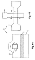
図7は、本発明の例示的な実施例によるFinFETデバイス710、720および730を含むウェーハの概略的な上面図である。
埋込酸化膜120はウェーハ(またはチップ)を示す。このウェーハの上には図示の3つのデバイス710、720および730が形成される。
デバイス710、720および730のうち少なくとも2つのデバイスの全体的なキャリア移動度が異なり得る。
デバイス710、720および730はすべてπゲートFinFET400、uゲートFinFET500、およびラウンドゲートFinFET600のいずれかのタイプのデバイスとすることができる。
あるいは、デバイス710、720および730は、ダブルゲートFinFET300、πゲートFinFET400、uゲートFinFET500およびラウンドゲートFinFET600のうち、複数の異なるタイプのデバイスを含み得る。
例えば、ダブルゲートFinFET300と、πゲートFinFET400、uゲートFinFET500およびラウンドゲートFinFET600の1つは同じフィンアスペクト比H/Wを有し得るが、それにも関わらず、FinFET400/500/600のさらなる垂直方向のチャネルにより、これらの全体的なキャリア移動度はどれも異なる。
例えば、全体的なキャリア移動度は、デバイス710/720のタイプに基づき異なり得る。
本発明の実施形態の一例においては、NMOSデバイスを、選択されたフィン・アスペクト比による全体的なキャリア移動度を有するようにし、同じウェーハ/チップ上のPMOSデバイスは、これとは異なるように選択されたフィン・アスペクト比による全体的なキャリア移動度を備えるものとする。これにより、NMOSデバイスのキャリア移動度がPMOSデバイスのキャリア移動度よりも大きさにおいて(すなわち、絶対値)より大きくなるように形成することができる。
あるいは、PMOSデバイスを、同じウェーハ/チップ上のNMOSデバイスの全体的なキャリア移動度より絶対値においてより大きい全体的なキャリア移動度で形成してもよい。
あるいは、デバイスの全体的なキャリア移動度がほぼ等しくなるように、NMOSデバイス(例えばデバイス710)およびPMOSデバイス(例えばデバイス720)のフィン・アスペクト比を選択してもよい。
例えば単一の回路素子内において、1つのFinFETデバイス710は第1フィン・アスペクト比H/W1を持ち得る。
回路素子内の他のFinFETデバイス720は、デバイス710/720間の駆動電流のバランスをとるために、第2フィン・アスペクト比H/W2を持ち得る。
本発明のある実施形態においては、(例えば図7のデバイス710のソース/ドレイン領域をデバイス720のドレイン/ソースに接続することによって)回路素子のデバイス710および720の異なるアスペクトのフィンを、電気的に接続してもよい。
例えば、1つの回路素子は1つ以上のFinFETデバイスを含んでいてもよい。また、FinFETデバイス710は第1フィン・アスペクト比H/W1を有し、このアスペクト比により定まる第1の全体的なキャリア移動度を有する。
分離した回路素子は、第2フィン・アスペクト比H/W2を有し、このアスペクト比により定まる第2の全体的なキャリア移動度を有する1つ以上のFinFETデバイス720を含み得る。
例えば、デバイス710および720は、それぞれCMOSデバイスのNMOSとPMOSの構成部分であり得る。
さらに、PMOSチャネル幅がNMOSチャネル幅に対して2:1の比率を有するような(単なる例示である)、既存のデザイン・ルールが存在していることがあるので、この方法により配置される、典型的な、プレーナMOSFETデバイスの駆動電流は、既存の関係を有している。
デバイス710および720の駆動電流の既存の関係を維持している一方で、デバイス710および720のフィン・アスペクト比を調整することにより、チャネル幅の比率を(例えば3:2に)異なるようにすることができる。
すなわち、デバイス710および720のそれぞれの幅W1、W2が3:2の比率を持つようにすることができ、デバイス710および720のそれぞれの高さH1およびH2を調整し、それぞれのフィン・アスペクト比H1/W1およびH2/W2が既存の駆動電流関係を得られるようにしてもよい。
すなわち、デバイス710および720のそれぞれの幅W1、W2が2:1の比率を有するようにすることができ、デバイス710および720のそれぞれの高さH1およびH2を調整し、それぞれのフィン・アスペクト比H1/W1およびH2/W2が新しい駆動電流関係(例えばデバイス710/720間の駆動電流が等しい関係)を生成するようにしてもよい。
同様に、フィン130の選択的なマスキングおよび露出している他のフィン130をエッチングしてこれらの高さを低くすることにより、異なるデバイス710/720のフィンの高さ(例えば、高さH1およびH2)が選択され得る。
生成した構造は、短チャネル耐性に優れているので有利である。さらに、本発明はフレキシビリティを増加すると共に、従来のプロセスに容易に統合することができる。
いくつかの実施形態においては、上述した他のものとは異なるラウンドゲートFinFETを形成することが望ましい。
図8Aないし図8Cは、本発明の他の実施形態によるラウンドゲートFinFET800の形成を示す断面図である。
図8Aは、(図2Bと同じように)フィンを形成した後のプロセス段階を示す断面図である。第1絶縁層830、第2絶縁層820、および基板810上にシリコン・フィン840を形成することができる。図8Aには示していないが、(図2Aと同じように)フィン840の一方の端部はソース及びドレイン領域と接続されている。
フィン840は、第2絶縁層820上に、実質的にサスペンド(浮遊)されている。
しかしながら、フィン840の端部はまだ第1絶縁層830に付着しており、図8Bに示すフィン840のサスペンドされた部分は、図示しないソース/ドレイン領域に隣接するフィン840の端部において第1絶縁層830に支持される。
ゲート材料層860は、後に形成されるゲート電極のゲート材料を含んでいるとともに、従来の化学蒸着法(CVD)を使用して、約500Åから約1000Åの範囲の厚みにたい積されたポリシリコンを含んでいてもよい。あるいは、ゲルマニウムまたはシリコンおよびゲルマニウムの組合わせのような他の半導体材料、または様々な金属を、層320のゲート材料として使用してもよい。
その後、ここに記載したように、ゲート材料層860をラウンドゲートFinFET800のゲートおよびゲート電極にパターン化することができる。
しかしながら、特にここに記載した詳細によることなく、本発明を実行することができる。その他、不必要に本発明の内容を不明瞭にしないように、周知のプロセス構造は詳細に記載していない。
ここに使用される、「ある(a)」と言う言葉は、1つ以上のものを含むように意図される。1つのものを示すような場合には「1つの(one)」またはこれに類する言葉を使用している。本発明の範囲は、請求の範囲およびこれらの均等物によって定義される。
Claims (10)
- 基板(110)と、
前記基板(110)上に形成される絶縁層(120)と、
前記絶縁層(120)上に形成されるとともに、第1フィンアスペクト比を有する第1フィン(130)を含む、前記絶縁層(120)上に形成される第1デバイス(710)と、
前記絶縁層(120)上に形成されるとともに、前記第1フィンアスペクト比と異なる第2フィンアスペクト比を有する第2フィン(130)を含む、前記絶縁層(120)上に形成される第2デバイス(720)と、
を含む、半導体デバイス(100)。 - 前記第1デバイス(710)はNMOSデバイスであり、前記第2デバイス(720)はPMOSデバイスである、請求項1記載の半導体デバイス(100)。
- 前記第1デバイス(710)および前記第2デバイス(720)は、単一の回路素子に含まれる、請求項1記載の半導体デバイス(100)。
- 前記第1デバイス(710)の前記第1フィン(130)の第1キャリア移動度は、前記第2デバイス(720)の前記第2フィン(130)の第2キャリア移動度と異なる、請求項1記載の半導体デバイス(100)。
- 前記第1デバイス(710)は、
前記第1フィン(130)の少なくとも3つの面上に形成される第1ゲート絶縁層(410)(510)(610)と、
前記第1フィン(130)の少なくとも3つの面上に形成される第1ゲート材料層(420)(520)(620)と、
をさらに含んでおり、
前記第2デバイス(720)は、
前記第2フィン(130)の少なくとも3つの面上に形成される第2ゲート絶縁層(410)(510)(610)と、
前記第2フィン(130)の少なくとも3つの面上に形成される第1ゲート材料層(420)(520)(620)と、
をさらに含む、請求項1記載の半導体デバイス(100)。 - 前記第1ゲート絶縁層(610)と前記第1ゲート材料層(620)は、前記第1フィン(130)の4つの面上に形成される、請求項5記載の半導体デバイス(100)。
- 前記第2ゲート絶縁層(610)と前記第2ゲート材料層(620)は、前記第2フィン(130)の4つの面上に形成される、請求項6記載の半導体デバイス(100)。
- 絶縁層(120)と、
前記絶縁層(120)上に形成され、第1高さおよび第1幅を有する第1フィン(130)、前記第1フィン(130)の少なくとも3つの面上に形成される第1ゲート絶縁層(410)(510)(610)、および前記第1ゲート絶縁層(410)(510)(610)に隣接する第1ゲート(430)(530)(630)を含む、前記絶縁層(120)上に形成される第1デバイス(710)と、
前記絶縁層(120)上に形成され、第2高さおよび第2幅を有する第2フィン(130)、前記第2フィン(130)の少なくとも3つの面上に形成される第2ゲート絶縁層(410)(510)(610)、および前記第2ゲート絶縁層(410)(510)(610)に隣接する第2ゲート(430)(530)(630)を含む、前記絶縁層(120)上に形成される第2デバイス(720)と、
を含み、前記第1高さと前記第1幅の第1比は、前記第2高さと前記第2幅の第2比と異なる、
半導体デバイス(100)。 - 前記絶縁層(120)上に形成され、第3高さおよび第3幅を有する第3フィン(130)、前記第3フィン(130)の少なくとも3つの面上に形成される第3ゲート絶縁層(410)(510)(610)、および前記第3ゲート絶縁層(410)(510)(610)に隣接する第3ゲート(430)(530)(630)を含む、前記絶縁層(120)上に形成される第3デバイス(730)をさらに含んでおり、
前記第3高さと前記第3幅の第3比は、前記第1比および前記第2比と異なる、請求項8記載の半導体デバイス(100)。 - 絶縁層(120)と、
前記絶縁層(120)上に形成され、第1高さおよび第1幅を有する第1フィン(130)を含む、前記絶縁層(120)上に形成されるN型デバイス(710)と、
前記絶縁層(120)上に形成され、第2高さおよび第2幅を有する第2フィン(130)を含む、前記絶縁層(120)上に形成されるP型デバイス(720)と、
を含んでおり、
前記第2幅は、前記第1幅の所定倍であり、
前記N型デバイス(710)のキャリア移動度が前記P型デバイス(720)のキャリア移動度とほぼ等しいように、前記第1高さおよび前記第2高さが形成される、
半導体デバイス(100)。
Applications Claiming Priority (2)
| Application Number | Priority Date | Filing Date | Title |
|---|---|---|---|
| US10/633,504 US7095065B2 (en) | 2003-08-05 | 2003-08-05 | Varying carrier mobility in semiconductor devices to achieve overall design goals |
| PCT/US2004/024590 WO2005034207A2 (en) | 2003-08-05 | 2004-07-28 | Varying carrier mobility on finfet active surfaces to achieve overall design goals |
Publications (2)
| Publication Number | Publication Date |
|---|---|
| JP2007501524A true JP2007501524A (ja) | 2007-01-25 |
| JP2007501524A5 JP2007501524A5 (ja) | 2007-08-02 |
Family
ID=34115850
Family Applications (1)
| Application Number | Title | Priority Date | Filing Date |
|---|---|---|---|
| JP2006522626A Pending JP2007501524A (ja) | 2003-08-05 | 2004-07-28 | 全体的な設計目標を達成すべく、半導体デバイス中のキャリア移動度の可変な半導体デバイス |
Country Status (8)
| Country | Link |
|---|---|
| US (1) | US7095065B2 (ja) |
| JP (1) | JP2007501524A (ja) |
| KR (1) | KR101042713B1 (ja) |
| CN (1) | CN1826696B (ja) |
| DE (1) | DE112004001442T5 (ja) |
| GB (1) | GB2419234B (ja) |
| TW (1) | TWI363421B (ja) |
| WO (1) | WO2005034207A2 (ja) |
Cited By (1)
| Publication number | Priority date | Publication date | Assignee | Title |
|---|---|---|---|---|
| US11670675B2 (en) | 2020-12-04 | 2023-06-06 | United Semiconductor Japan Co., Ltd. | Semiconductor device |
Families Citing this family (21)
| Publication number | Priority date | Publication date | Assignee | Title |
|---|---|---|---|---|
| US6855607B2 (en) * | 2003-06-12 | 2005-02-15 | Advanced Micro Devices, Inc. | Multi-step chemical mechanical polishing of a gate area in a FinFET |
| US6946377B2 (en) * | 2003-10-29 | 2005-09-20 | Texas Instruments Incorporated | Multiple-gate MOSFET device with lithography independent silicon body thickness and methods for fabricating the same |
| US7087471B2 (en) * | 2004-03-15 | 2006-08-08 | International Business Machines Corporation | Locally thinned fins |
| FR2899017A1 (fr) * | 2006-03-21 | 2007-09-28 | St Microelectronics Sa | Procede de realisation d'un transistor a canal comprenant du germanium |
| EP2013900A1 (en) * | 2006-04-26 | 2009-01-14 | Koninklijke Philips Electronics N.V. | Non-volatile memory device |
| US7517764B2 (en) * | 2006-06-29 | 2009-04-14 | International Business Machines Corporation | Bulk FinFET device |
| US8883597B2 (en) * | 2007-07-31 | 2014-11-11 | Taiwan Semiconductor Manufacturing Company, Ltd. | Method of fabrication of a FinFET element |
| FR2928028B1 (fr) * | 2008-02-27 | 2011-07-15 | St Microelectronics Crolles 2 | Procede de fabrication d'un dispositif semi-conducteur a grille enterree et circuit integre correspondant. |
| FR2928029B1 (fr) * | 2008-02-27 | 2011-04-08 | St Microelectronics Crolles 2 | Procede de fabrication d'un dispositif semi-conducteur a grille enterree et circuit integre correspondant. |
| JP5718585B2 (ja) * | 2010-05-19 | 2015-05-13 | ピーエスフォー ルクスコ エスエイアールエルPS4 Luxco S.a.r.l. | 半導体装置及びその製造方法、並びにデータ処理システム |
| US20120146101A1 (en) * | 2010-12-13 | 2012-06-14 | Chun-Hsien Lin | Multi-gate transistor devices and manufacturing method thereof |
| US9059001B2 (en) * | 2011-12-16 | 2015-06-16 | Taiwan Semiconductor Manufacturing Company, Ltd. | Semiconductor device with biased feature |
| WO2013095550A1 (en) | 2011-12-22 | 2013-06-27 | Intel Corporation | Semiconductor device having a necked semiconductor body and method of forming semiconductor bodies of varying width |
| CN103474461B (zh) * | 2012-06-06 | 2016-01-06 | 中芯国际集成电路制造(上海)有限公司 | 鳍式场效应管及其形成方法 |
| US8841189B1 (en) * | 2013-06-14 | 2014-09-23 | International Business Machines Corporation | Transistor having all-around source/drain metal contact channel stressor and method to fabricate same |
| US9425275B2 (en) | 2014-06-13 | 2016-08-23 | Samsung Electronics Co., Ltd. | Integrated circuit chips having field effect transistors with different gate designs |
| US9112032B1 (en) * | 2014-06-16 | 2015-08-18 | Globalfoundries Inc. | Methods of forming replacement gate structures on semiconductor devices |
| US9590074B1 (en) | 2015-12-05 | 2017-03-07 | International Business Machines Corporation | Method to prevent lateral epitaxial growth in semiconductor devices |
| US10879125B2 (en) | 2018-12-27 | 2020-12-29 | Nanya Technology Corporation | FinFET structure and method of manufacturing the same |
| CN115669260A (zh) * | 2021-05-12 | 2023-01-31 | 长江存储科技有限责任公司 | 具有三维晶体管的存储器外围电路及其形成方法 |
| CN113764348B (zh) * | 2021-09-07 | 2023-06-16 | 上海集成电路装备材料产业创新中心有限公司 | 鳍式半导体器件的制备方法 |
Citations (10)
| Publication number | Priority date | Publication date | Assignee | Title |
|---|---|---|---|---|
| JPS61112364A (ja) * | 1984-11-07 | 1986-05-30 | Hitachi Ltd | 半導体装置 |
| JPH03250770A (ja) * | 1990-02-28 | 1991-11-08 | Sony Corp | 半導体装置 |
| JPH06342911A (ja) * | 1993-06-01 | 1994-12-13 | Oki Electric Ind Co Ltd | 半導体装置の製造方法 |
| JP2001093987A (ja) * | 1999-07-29 | 2001-04-06 | Stmicroelectronics Inc | Si基板上のGaAs/Geの新規なCMOS回路 |
| JP2002118255A (ja) * | 2000-07-31 | 2002-04-19 | Toshiba Corp | 半導体装置およびその製造方法 |
| JP2002151688A (ja) * | 2000-08-28 | 2002-05-24 | Mitsubishi Electric Corp | Mos型半導体装置およびその製造方法 |
| US20020197803A1 (en) * | 2001-06-21 | 2002-12-26 | Amberwave Systems Corporation | Enhancement of p-type metal-oxide-semiconductor field effect transistors |
| JP2003163356A (ja) * | 2001-10-05 | 2003-06-06 | Internatl Business Mach Corp <Ibm> | 二重ゲート・トランジスタおよびその製造方法 |
| JP2003188273A (ja) * | 2001-12-13 | 2003-07-04 | Tadahiro Omi | 相補型mis装置 |
| US20040110331A1 (en) * | 2002-12-06 | 2004-06-10 | Yee-Chia Yeo | CMOS inverters configured using multiple-gate transistors |
Family Cites Families (4)
| Publication number | Priority date | Publication date | Assignee | Title |
|---|---|---|---|---|
| US5391506A (en) | 1992-01-31 | 1995-02-21 | Kawasaki Steel Corporation | Manufacturing method for semiconductor devices with source/drain formed in substrate projection. |
| US20020011612A1 (en) | 2000-07-31 | 2002-01-31 | Kabushiki Kaisha Toshiba | Semiconductor device and method for manufacturing the same |
| US6657259B2 (en) | 2001-12-04 | 2003-12-02 | International Business Machines Corporation | Multiple-plane FinFET CMOS |
| US6909147B2 (en) * | 2003-05-05 | 2005-06-21 | International Business Machines Corporation | Multi-height FinFETS |
-
2003
- 2003-08-05 US US10/633,504 patent/US7095065B2/en not_active Expired - Lifetime
-
2004
- 2004-07-28 WO PCT/US2004/024590 patent/WO2005034207A2/en active Application Filing
- 2004-07-28 DE DE112004001442T patent/DE112004001442T5/de not_active Withdrawn
- 2004-07-28 KR KR1020067002327A patent/KR101042713B1/ko not_active IP Right Cessation
- 2004-07-28 GB GB0526405A patent/GB2419234B/en not_active Expired - Fee Related
- 2004-07-28 JP JP2006522626A patent/JP2007501524A/ja active Pending
- 2004-07-28 CN CN200480021176XA patent/CN1826696B/zh active Active
- 2004-08-03 TW TW093123171A patent/TWI363421B/zh not_active IP Right Cessation
Patent Citations (10)
| Publication number | Priority date | Publication date | Assignee | Title |
|---|---|---|---|---|
| JPS61112364A (ja) * | 1984-11-07 | 1986-05-30 | Hitachi Ltd | 半導体装置 |
| JPH03250770A (ja) * | 1990-02-28 | 1991-11-08 | Sony Corp | 半導体装置 |
| JPH06342911A (ja) * | 1993-06-01 | 1994-12-13 | Oki Electric Ind Co Ltd | 半導体装置の製造方法 |
| JP2001093987A (ja) * | 1999-07-29 | 2001-04-06 | Stmicroelectronics Inc | Si基板上のGaAs/Geの新規なCMOS回路 |
| JP2002118255A (ja) * | 2000-07-31 | 2002-04-19 | Toshiba Corp | 半導体装置およびその製造方法 |
| JP2002151688A (ja) * | 2000-08-28 | 2002-05-24 | Mitsubishi Electric Corp | Mos型半導体装置およびその製造方法 |
| US20020197803A1 (en) * | 2001-06-21 | 2002-12-26 | Amberwave Systems Corporation | Enhancement of p-type metal-oxide-semiconductor field effect transistors |
| JP2003163356A (ja) * | 2001-10-05 | 2003-06-06 | Internatl Business Mach Corp <Ibm> | 二重ゲート・トランジスタおよびその製造方法 |
| JP2003188273A (ja) * | 2001-12-13 | 2003-07-04 | Tadahiro Omi | 相補型mis装置 |
| US20040110331A1 (en) * | 2002-12-06 | 2004-06-10 | Yee-Chia Yeo | CMOS inverters configured using multiple-gate transistors |
Cited By (1)
| Publication number | Priority date | Publication date | Assignee | Title |
|---|---|---|---|---|
| US11670675B2 (en) | 2020-12-04 | 2023-06-06 | United Semiconductor Japan Co., Ltd. | Semiconductor device |
Also Published As
| Publication number | Publication date |
|---|---|
| TWI363421B (en) | 2012-05-01 |
| WO2005034207A3 (en) | 2005-06-30 |
| KR20060054420A (ko) | 2006-05-22 |
| US20050029603A1 (en) | 2005-02-10 |
| WO2005034207A2 (en) | 2005-04-14 |
| GB2419234B (en) | 2007-02-21 |
| CN1826696B (zh) | 2011-01-26 |
| CN1826696A (zh) | 2006-08-30 |
| GB2419234A (en) | 2006-04-19 |
| US7095065B2 (en) | 2006-08-22 |
| KR101042713B1 (ko) | 2011-06-20 |
| GB0526405D0 (en) | 2006-02-08 |
| DE112004001442T5 (de) | 2006-06-08 |
| TW200509390A (en) | 2005-03-01 |
Similar Documents
| Publication | Publication Date | Title |
|---|---|---|
| US6787439B2 (en) | Method using planarizing gate material to improve gate critical dimension in semiconductor devices | |
| KR101637679B1 (ko) | Fⅰnfet을 형성하기 위한 메커니즘들을 포함하는 반도체 디바이스및 그 형성 방법 | |
| KR101504311B1 (ko) | 맨드렐 산화 공정을 사용하여 finfet 반도체 디바이스용 핀들을 형성하는 방법 | |
| US6645797B1 (en) | Method for forming fins in a FinFET device using sacrificial carbon layer | |
| US6709982B1 (en) | Double spacer FinFET formation | |
| KR100532353B1 (ko) | 핀 전계 효과 트랜지스터 및 그 제조방법 | |
| US7256455B2 (en) | Double gate semiconductor device having a metal gate | |
| JP5409997B2 (ja) | FinFETデバイス中にゲートを形成する方法、および半導体デバイスの製造方法 | |
| KR101042713B1 (ko) | 전체 설계 목적들을 달성하기 위해 핀펫 활성 표면들 상의 캐리어 이동도의 가변 | |
| US6706571B1 (en) | Method for forming multiple structures in a semiconductor device | |
| US6787854B1 (en) | Method for forming a fin in a finFET device | |
| KR101112046B1 (ko) | 자기 정렬된 다마신 게이트 | |
| US6998301B1 (en) | Method for forming a tri-gate MOSFET | |
| JP2006505950A (ja) | 分離した複数のゲートを有するダブルゲート半導体デバイス | |
| US20070048947A1 (en) | Multi-structured Si-fin and method of manufacture | |
| US20060170066A1 (en) | Hybrid-fet and its application as sram | |
| US20070069254A1 (en) | Multiple-gate MOS transistor using Si substrate and method of manufacturing the same | |
| US6936882B1 (en) | Selective silicidation of gates in semiconductor devices to achieve multiple threshold voltages | |
| US6911697B1 (en) | Semiconductor device having a thin fin and raised source/drain areas | |
| US7416925B2 (en) | Doped structure for finfet devices | |
| CN104347508B (zh) | 半导体结构及其形成方法 | |
| KR100491979B1 (ko) | 초미세 채널 전계 효과 트랜지스터 및 그 제조방법 | |
| KR20020096654A (ko) | 이중 게이트 mosfet 및 그 제조방법 | |
| JP2022552417A (ja) | 水平ゲートオールアラウンド(hGAA)ナノワイヤ及びナノスラブトランジスタ | |
| US7112847B1 (en) | Smooth fin topology in a FinFET device |
Legal Events
| Date | Code | Title | Description |
|---|---|---|---|
| A521 | Written amendment |
Free format text: JAPANESE INTERMEDIATE CODE: A523 Effective date: 20070613 |
|
| A621 | Written request for application examination |
Free format text: JAPANESE INTERMEDIATE CODE: A621 Effective date: 20070613 |
|
| RD03 | Notification of appointment of power of attorney |
Free format text: JAPANESE INTERMEDIATE CODE: A7423 Effective date: 20100421 |
|
| RD05 | Notification of revocation of power of attorney |
Free format text: JAPANESE INTERMEDIATE CODE: A7425 Effective date: 20100902 |
|
| A977 | Report on retrieval |
Free format text: JAPANESE INTERMEDIATE CODE: A971007 Effective date: 20110415 |
|
| A131 | Notification of reasons for refusal |
Free format text: JAPANESE INTERMEDIATE CODE: A131 Effective date: 20110427 |
|
| A601 | Written request for extension of time |
Free format text: JAPANESE INTERMEDIATE CODE: A601 Effective date: 20110727 |
|
| A602 | Written permission of extension of time |
Free format text: JAPANESE INTERMEDIATE CODE: A602 Effective date: 20110803 |
|
| A521 | Written amendment |
Free format text: JAPANESE INTERMEDIATE CODE: A523 Effective date: 20110829 |
|
| A131 | Notification of reasons for refusal |
Free format text: JAPANESE INTERMEDIATE CODE: A131 Effective date: 20120314 |
|
| A02 | Decision of refusal |
Free format text: JAPANESE INTERMEDIATE CODE: A02 Effective date: 20120822 |