JP2007241237A - 二層金属ラインを有する薄膜トランジスタディスプレイアレイを製造するための方法 - Google Patents
二層金属ラインを有する薄膜トランジスタディスプレイアレイを製造するための方法 Download PDFInfo
- Publication number
- JP2007241237A JP2007241237A JP2006294422A JP2006294422A JP2007241237A JP 2007241237 A JP2007241237 A JP 2007241237A JP 2006294422 A JP2006294422 A JP 2006294422A JP 2006294422 A JP2006294422 A JP 2006294422A JP 2007241237 A JP2007241237 A JP 2007241237A
- Authority
- JP
- Japan
- Prior art keywords
- patterned
- layer
- conductive
- conductive lines
- metal layer
- Prior art date
- Legal status (The legal status is an assumption and is not a legal conclusion. Google has not performed a legal analysis and makes no representation as to the accuracy of the status listed.)
- Granted
Links
Images


Classifications
-
- H—ELECTRICITY
- H10—SEMICONDUCTOR DEVICES; ELECTRIC SOLID-STATE DEVICES NOT OTHERWISE PROVIDED FOR
- H10W—GENERIC PACKAGES, INTERCONNECTIONS, CONNECTORS OR OTHER CONSTRUCTIONAL DETAILS OF DEVICES COVERED BY CLASS H10
- H10W20/00—Interconnections in chips, wafers or substrates
- H10W20/01—Manufacture or treatment
- H10W20/031—Manufacture or treatment of conductive parts of the interconnections
-
- H—ELECTRICITY
- H10—SEMICONDUCTOR DEVICES; ELECTRIC SOLID-STATE DEVICES NOT OTHERWISE PROVIDED FOR
- H10D—INORGANIC ELECTRIC SEMICONDUCTOR DEVICES
- H10D86/00—Integrated devices formed in or on insulating or conducting substrates, e.g. formed in silicon-on-insulator [SOI] substrates or on stainless steel or glass substrates
- H10D86/40—Integrated devices formed in or on insulating or conducting substrates, e.g. formed in silicon-on-insulator [SOI] substrates or on stainless steel or glass substrates characterised by multiple TFTs
- H10D86/441—Interconnections, e.g. scanning lines
-
- H—ELECTRICITY
- H10—SEMICONDUCTOR DEVICES; ELECTRIC SOLID-STATE DEVICES NOT OTHERWISE PROVIDED FOR
- H10D—INORGANIC ELECTRIC SEMICONDUCTOR DEVICES
- H10D86/00—Integrated devices formed in or on insulating or conducting substrates, e.g. formed in silicon-on-insulator [SOI] substrates or on stainless steel or glass substrates
- H10D86/40—Integrated devices formed in or on insulating or conducting substrates, e.g. formed in silicon-on-insulator [SOI] substrates or on stainless steel or glass substrates characterised by multiple TFTs
- H10D86/60—Integrated devices formed in or on insulating or conducting substrates, e.g. formed in silicon-on-insulator [SOI] substrates or on stainless steel or glass substrates characterised by multiple TFTs wherein the TFTs are in active matrices
Landscapes
- Thin Film Transistor (AREA)
- Liquid Crystal (AREA)
- Devices For Indicating Variable Information By Combining Individual Elements (AREA)
- Internal Circuitry In Semiconductor Integrated Circuit Devices (AREA)
Abstract
【解決手段】TFTアレイを製造するための方法は、基板と、複数の第1の導電性ラインと複数の第2の導電性ラインとを有し基板上にパターニングされた第1の金属層と、パターニングされた第1の金属層の上の絶縁層と、パターニングされたシリコン層と、パターニングされたシリコン層の上のパターニングされた保護層と、パターニングされた保護層の上のパターニングされたドープシリコン層及びパターニングされた第2の金属層とを準備し、パターニングされたシリコン層の露出した部分と第1の導電性ラインと第2の導電性ラインの露出した部分を埋め、パターニングされた第2の金属層が、複数の第3の導電性ラインと複数の第4の導電性ラインを備え、そのそれぞれが、複数の第1の導電性ラインと複数の第2の導電性ラインの1つにそれぞれに対応する。
【選択図】図1H
Description
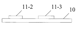
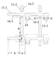
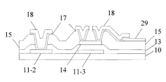
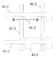
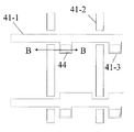
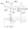
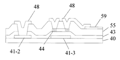
11、31、41 第1の金属層
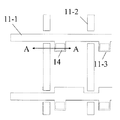
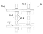
11−1、31−1、41−1、48−1 第1の導電性ライン
11−2、31−2、41−2、48−2 第2の導電性ライン
11−3、41−3 ゲート電極
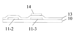
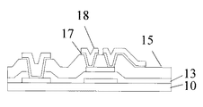
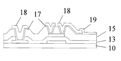
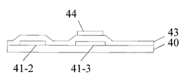
13、43 絶縁層
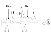
14、44 シリコン層
15、45、55 保護層
17 ドープシリコン層
18、48 第2の金属層
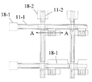
18−1、48−1 第3の導電性ライン
18−2、48−2 第4の導電性ライン
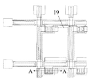
19、29、49、59 画素電極層
16−1、16−2、16−3、46−1、46−2、46−3 トレンチ
36−1、36−2 コンタクトホール
Claims (30)
- 薄膜トランジスタ(「TFT」)アレイを製造するための方法であって、
基板を用意するステップと、
前記基板上にパターニングされた第1の金属層を形成し、該パターニングされた第1の金属層が、複数の第1の導電性ラインと該第1の導電性ラインに直交して配置される複数の第2の導電性ラインとを有し、前記第1の導電性ラインのそれぞれが、複数のゲート電極を有し、該ゲート電極のそれぞれが、1つの前記第1の導電性ラインと1つの前記第2の導電性ラインの交点の近くに配置されるステップと、
前記パターニングされた第1の金属層の上に絶縁層を形成するステップと、
パターニングされたシリコン層を形成するステップと、
前記パターニングされたシリコン層と前記パターニングされた第1の金属層の上にパターニングされた保護層を形成し、前記パターニングされたシリコン層の一部とそれぞれ1つの前記第1の導電性ライン及びそれぞれ1つの前記第2の導電性ラインの一部とを露出させるステップと、
前記パターニングされた保護層の上にパターニングされたドープシリコン層とパターニングされた第2の金属層とを形成し、前記パターニングされたシリコン層の露出した部分と前記第1の導電性ライン及び前記第2の導電性ラインの露出した部分とを埋め、前記パターニングされた第2の金属層が、複数の第3の導電性ラインと複数の第4の導電性ラインとを有し、前記第3の導電性ラインと前記第4の導電性ラインのそれぞれが、前記複数の第1の導電性ラインの1つと前記複数の第2の導電性ラインの1つにそれぞれに対応するステップと、
を備えていることを特徴とする方法。 - 前記パターニングされた第2の金属層と前記パターニングされた保護層の上にパターニングされた画素電極層を形成するステップをさらに備えていることを特徴とする請求項1に記載の方法。
- 前記パターニングされたシリコン層の上に保護層を形成するステップと、
前記保護層の上にパターニングされた画素電極層を形成するステップと、
前記保護層をパターニングし、前記パターニングされたシリコン層の一部と前記第1の導電性ライン又は第2の導電性ラインの一部とを露出させるステップと、
をさらに備えていることを特徴とする請求項1に記載の方法。 - 前記パターニングされた保護層の上にパターニングされた画素電極層を形成するステップと、
前記パターニングされた保護層と前記パターニングされた画素電極層の上に、パターニングされたドープシリコン層とパターニングされた第2の金属層とを形成し、前記パターニングされたドープシリコン層の露出した部分と前記第1の導電性ライン又は第2の導電性ラインの露出した部分とを埋めるステップと、
をさらに備えていることを特徴とする請求項1に記載の方法。 - 前記パターニングされた第1の金属層の前記第1の導電性ラインと第2の導電性ラインの少なくとも1つの上の前記保護層と前記絶縁層にトレンチを形成するステップをさらに備えていることを特徴とする請求項1に記載の方法。
- 前記トレンチを通じて前記パターニングされた第1の金属層と前記パターニングされた第2の金属層とを電気的に接続させるステップをさらに備えていることを特徴とする請求項5に記載の方法。
- 前記パターニングされた第1の金属層の前記第1の導電性ラインと前記第2の導電性ラインの少なくとも1つの上の前記保護層と前記絶縁層に複数のコンタクトホールを形成するステップをさらに備えていることを特徴とする請求項1に記載の方法。
- 前記複数のコンタクトホールを通じて前記パターニングされた第1の金属層と前記パターニングされた第2の金属層とを電気的に接続させるステップをさらに備えていることを特徴とする請求項7に記載の方法。
- 前記パターニングされた第1の金属層のそれぞれの前記第2の導電性ラインが、互いに離れている複数の分岐ラインを備えていることを特徴とする請求項1に記載の方法。
- 前記それぞれの分岐ラインと、同じ前記第2の導電性ライン上に配置され直接隣接する分岐ラインとの間の距離に対する前記分岐ラインのそれぞれの長さの比が、約2から20の範囲であることを特徴とする請求項9に記載の方法。
- 前記パターニングされた第2の金属層のそれぞれの前記第3の導電性ラインが、互いに離れている複数の分岐ラインを備えていることを特徴とする請求項1に記載の方法。
- 前記それぞれの分岐ラインと、同じ前記第3の導電性ライン上に配置され直接隣接する分岐ラインとの間の距離に対する前記分岐ラインのそれぞれの長さの比が、約2から20の範囲であることを特徴とする請求項11に記載の方法。
- アモルファスシリコン層又は多結晶シリコン層の1つを有するパターニングされたシリコン層を形成するステップをさらに備えていることを特徴とする請求項1に記載の方法。
- 薄膜トランジスタ(「TFT」)アレイを製造するための方法であって、
基板を用意するステップと、
前記基板上にパターニングされた第1の金属層を形成し、該パターニングされた第1の金属層が、複数の第1の導電性ラインと該第1の導電性ラインに直交して配置される複数の第2の導電性ラインとを有し、前記第1の導電性ラインのそれぞれが、複数のゲート電極を有し、該ゲート電極のそれぞれが、1つの前記第1の導電性ラインと1つの前記第2の導電性ラインの交点の近くに配置されるステップと、
前記パターニングされた第1の金属層の上に絶縁層を形成するステップと、
パターニングされたシリコン層を形成するステップと、
前記パターニングされたシリコン層と前記パターニングされた第1の金属層の上にパターニングされた保護層を形成し、前記パターニングされたシリコン層の一部と前記第1の導電性ライン及び前記第2の導電性ラインのそれぞれの一部とを露出させるステップと、
前記パターニングされたシリコン層の露出した部分の中へ不純物をドープするステップと、
前記パターニングされた保護層の上にパターニングされた第2の金属層を形成し、前記パターニングされたシリコン層の露出した部分と前記第1の導電性ライン又は第2の導電性ラインの露出した部分とを埋め、前記パターニングされた第2の金属層が、複数の第3の導電性ラインと複数の第4の導電性ラインとを有し、前記第3の導電性ラインと前記第4の導電性ラインのそれぞれが、前記パターニングされた第1の金属層の前記複数の第1の導電性ラインの1つと前記複数の第2の導電性ラインの1つにそれぞれに対応するステップと、
を備えていることを特徴とする方法。 - 前記パターニングされた第2の金属層と前記パターニングされた保護層の上にパターニングされた画素電極層を形成するステップをさらに備えていることを特徴とする請求項14に記載の方法。
- 前記パターニングされたシリコン層の上に保護層を形成するステップと、
前記保護層の上にパターニングされた画素電極層を形成するステップと、
前記保護層をパターニングし、前記パターニングされたシリコン層の一部と前記第1の導電性ライン又は第2の導電性ラインの一部とを露出させるステップと、
をさらに備えていることを特徴とする請求項14に記載の方法。 - 前記パターニングされたシリコン層の露出した部分の中へ不純物をドープするステップと、
前記パターニングされた保護層の上にパターニングされた画素電極層を形成するステップと、
前記パターニングされた保護層と前記パターニングされた画素電極層の上にパターニングされた第2の金属層を形成し、前記パターニングされたシリコン層の露出した部分と前記第1の導電性ライン又は第2の導電性ラインの露出した部分とを埋めるステップと、
をさらに備えていることを特徴とする請求項14に記載の方法。 - 前記パターニングされた第1の金属層の前記第1の導電性ライン又は第2の導電性ラインの少なくとも1つの上の前記保護層と前記絶縁層にトレンチを形成するステップをさらに備えていることを特徴とする請求項14に記載の方法。
- 前記トレンチを通じて前記パターニングされた第1の金属層と前記パターニングされた第2の金属層とを電気的に接続させるステップをさらに備えていることを特徴とする請求項18に記載の方法。
- 前記パターニングされた第1の金属層の前記第1の導電性ラインと前記第2の導電性ラインの少なくとも1つの上の前記保護層と前記絶縁層に複数のコンタクトホールを形成するステップをさらに備えていることを特徴とする請求項14に記載の方法。
- 前記複数のコンタクトホールを通じて前記パターニングされた第1の金属層と前記パターニングされた第2の金属層とを電気的に接続させるステップをさらに備えていることを特徴とする請求項20に記載の方法。
- 前記パターニングされた第1の金属層のそれぞれの前記第2の導電性ラインが、互いに離れている複数の分岐ラインを備えていることを特徴とする請求項14に記載の方法。
- 前記それぞれの分岐ラインと、同じ前記第2の導電性ライン上に配置され直接隣接する分岐ラインとの間の距離に対する前記分岐ラインのそれぞれの長さの比が、約2から20の範囲であることを特徴とする請求項22に記載の方法。
- 前記パターニングされた第2の金属層のそれぞれの前記第3の導電性ラインが、互いに離れている複数の分岐ラインを備えていることを特徴とする請求項14に記載の方法。
- 前記それぞれの分岐ラインと、同じ前記第1の導電性ライン上に配置され直接隣接する分岐ラインとの間の距離に対する前記分岐ラインのそれぞれの長さの比が、約2から20の範囲であることを特徴とする請求項24に記載の方法。
- アモルファスシリコン層又は多結晶シリコン層の1つを有するパターニングされたシリコン層を形成するステップをさらに備えていることを特徴とする請求項14に記載の方法。
- 薄膜トランジスタ(「TFT」)アレイを製造するための方法であって、
基板を用意するステップと、
前記基板上にパターニングされた第1の金属層を形成し、該パターニングされた第1の金属層が、複数の第1の導電性ラインと該第1の導電性ラインに直交して配置される複数の第2の導電性ラインとを有し、前記第2の導電性ラインのそれぞれが、互いに離れている複数の分岐ラインを有するステップと、
前記パターニングされた第1の金属層の上に絶縁層を形成するステップと、
前記絶縁層の上にパターニングされたシリコン層を形成するステップと、
それぞれの前記第1の導電性ラインの一部と前記パターニングされた第1の金属層のそれぞれの前記第2の導電性ラインの分岐ラインを露出させるステップと、
前記パターニングされたシリコン層の上にパターニングされた第2の金属層を形成し、それぞれの前記第1の導電性ラインの露出した部分とそれぞれの前記第2の導電性ラインの露出した部分を埋め、前記パターニングされた第2の金属層が、複数の第3の導電性ラインと複数の第4の導電性ラインとを有し、前記第3の導電性ラインと前記第4の導電性ラインのそれぞれが、前記パターニングされた第1の金属層の前記複数の第1の導電性ラインの1つと前記複数の第2の導電性ラインの1つにそれぞれに対応するステップと、
を備えていることを特徴とする方法。 - 前記パターニングされた第2の金属層のそれぞれの前記第3の導電性ラインが、互いに離れている複数の分岐ラインを備えていることを特徴とする請求項27に記載の方法。
- 前記それぞれの分岐ラインと、前記パターニングされた第1の金属層の同じ前記第3の導電性ライン上に配置され直接隣接する分岐ラインとの間の距離に対する前記それぞれの分岐ラインの長さの比が、約2から20の範囲であることを特徴とする請求項28に記載の方法。
- 前記それぞれの分岐ラインと、前記パターニングされた第2の金属層の同じ前記第4の導電性ライン上に配置され直接隣接する分岐ラインとの間の距離に対する前記それぞれの分岐ラインの長さの比が、約2から20の範囲であることを特徴とする請求項27に記載の方法。
Applications Claiming Priority (1)
| Application Number | Priority Date | Filing Date | Title |
|---|---|---|---|
| US11/369,624 US7638371B2 (en) | 2006-03-07 | 2006-03-07 | Method for manufacturing thin film transistor display array with dual-layer metal line |
Publications (2)
| Publication Number | Publication Date |
|---|---|
| JP2007241237A true JP2007241237A (ja) | 2007-09-20 |
| JP4495712B2 JP4495712B2 (ja) | 2010-07-07 |
Family
ID=38479454
Family Applications (1)
| Application Number | Title | Priority Date | Filing Date |
|---|---|---|---|
| JP2006294422A Expired - Fee Related JP4495712B2 (ja) | 2006-03-07 | 2006-10-30 | 二層金属ラインを有する薄膜トランジスタディスプレイアレイを製造するための方法 |
Country Status (4)
| Country | Link |
|---|---|
| US (1) | US7638371B2 (ja) |
| JP (1) | JP4495712B2 (ja) |
| CN (1) | CN100477171C (ja) |
| TW (1) | TWI356458B (ja) |
Cited By (4)
| Publication number | Priority date | Publication date | Assignee | Title |
|---|---|---|---|---|
| JP2012244123A (ja) * | 2011-05-24 | 2012-12-10 | Semiconductor Energy Lab Co Ltd | 半導体装置 |
| JP2013219348A (ja) * | 2012-03-14 | 2013-10-24 | Semiconductor Energy Lab Co Ltd | 半導体装置 |
| WO2016195001A1 (ja) * | 2015-06-04 | 2016-12-08 | シャープ株式会社 | アクティブマトリクス基板 |
| JP2019003127A (ja) * | 2017-06-19 | 2019-01-10 | 株式会社ジャパンディスプレイ | 液晶表示装置 |
Families Citing this family (8)
| Publication number | Priority date | Publication date | Assignee | Title |
|---|---|---|---|---|
| KR101682078B1 (ko) * | 2010-07-30 | 2016-12-05 | 삼성디스플레이 주식회사 | 박막 트랜지스터 표시판의 제조 방법 |
| US9239502B2 (en) | 2011-12-23 | 2016-01-19 | Au Optronics Corporation | Pixel structure with data line, scan line and gate electrode formed on the same layer and manufacturing method thereof |
| TWI457672B (zh) * | 2011-12-23 | 2014-10-21 | Au Optronics Corp | 畫素結構及其製造方法 |
| US20140036188A1 (en) * | 2012-08-01 | 2014-02-06 | Cheng-Hung Chen | Liquid Crystal Display Device, Array Substrate and Manufacturing Method Thereof |
| CN102809859B (zh) * | 2012-08-01 | 2014-12-31 | 深圳市华星光电技术有限公司 | 液晶显示装置、阵列基板及其制作方法 |
| CN104505392A (zh) * | 2014-12-29 | 2015-04-08 | 合肥鑫晟光电科技有限公司 | 阵列基板及其制作方法、阵列基板的修复方法、显示装置 |
| CN110853531B (zh) | 2019-11-21 | 2021-11-05 | 京东方科技集团股份有限公司 | 显示用驱动背板及其制备方法、显示面板 |
| EP4138126A4 (en) * | 2021-07-09 | 2023-07-19 | Changxin Memory Technologies, Inc. | Semiconductor test structure and forming method therefor |
Citations (2)
| Publication number | Priority date | Publication date | Assignee | Title |
|---|---|---|---|---|
| JP2000002884A (ja) * | 1998-06-15 | 2000-01-07 | Sharp Corp | アクティブマトリクス基板およびその製造方法 |
| JP2000352940A (ja) * | 1999-06-11 | 2000-12-19 | Toshiba Corp | マトリクスアレイ基板 |
Family Cites Families (10)
| Publication number | Priority date | Publication date | Assignee | Title |
|---|---|---|---|---|
| FR2605442B1 (fr) | 1986-10-17 | 1988-12-09 | Thomson Csf | Ecran de visualisation electrooptique a transistors de commande et procede de realisation |
| US20020020840A1 (en) * | 2000-03-10 | 2002-02-21 | Setsuo Nakajima | Semiconductor device and manufacturing method thereof |
| KR100684577B1 (ko) * | 2000-06-12 | 2007-02-20 | 엘지.필립스 엘시디 주식회사 | 반사투과형 액정표시장치 및 그 제조방법 |
| KR100939560B1 (ko) * | 2003-06-30 | 2010-01-29 | 엘지디스플레이 주식회사 | 액정표시장치용 어레이기판과 제조방법 |
| KR100938887B1 (ko) * | 2003-06-30 | 2010-01-27 | 엘지디스플레이 주식회사 | 액정표시장치용 어레이기판과 그 제조방법 |
| TWI220775B (en) * | 2003-10-03 | 2004-09-01 | Ind Tech Res Inst | Multi-layered complementary wire structure and manufacturing method thereof |
| US7161226B2 (en) | 2003-10-20 | 2007-01-09 | Industrial Technology Research Institute | Multi-layered complementary wire structure and manufacturing method thereof |
| TWI282969B (en) * | 2004-04-29 | 2007-06-21 | Au Optronics Corp | Thin film transistor array and fabricating method thereof |
| KR101043992B1 (ko) * | 2004-08-12 | 2011-06-24 | 엘지디스플레이 주식회사 | 액정표시소자 및 그 제조방법 |
| KR20060016920A (ko) * | 2004-08-19 | 2006-02-23 | 삼성전자주식회사 | 박막 트랜지스터 표시판 및 그 제조 방법 |
-
2006
- 2006-03-07 US US11/369,624 patent/US7638371B2/en not_active Expired - Fee Related
- 2006-08-23 TW TW095131054A patent/TWI356458B/zh not_active IP Right Cessation
- 2006-09-29 CN CN200610140665.8A patent/CN100477171C/zh not_active Expired - Fee Related
- 2006-10-30 JP JP2006294422A patent/JP4495712B2/ja not_active Expired - Fee Related
Patent Citations (2)
| Publication number | Priority date | Publication date | Assignee | Title |
|---|---|---|---|---|
| JP2000002884A (ja) * | 1998-06-15 | 2000-01-07 | Sharp Corp | アクティブマトリクス基板およびその製造方法 |
| JP2000352940A (ja) * | 1999-06-11 | 2000-12-19 | Toshiba Corp | マトリクスアレイ基板 |
Cited By (7)
| Publication number | Priority date | Publication date | Assignee | Title |
|---|---|---|---|---|
| JP2012244123A (ja) * | 2011-05-24 | 2012-12-10 | Semiconductor Energy Lab Co Ltd | 半導体装置 |
| US9525023B2 (en) | 2011-05-24 | 2016-12-20 | Semiconductor Energy Laboratory Co., Ltd. | Semiconductor device |
| JP2013219348A (ja) * | 2012-03-14 | 2013-10-24 | Semiconductor Energy Lab Co Ltd | 半導体装置 |
| WO2016195001A1 (ja) * | 2015-06-04 | 2016-12-08 | シャープ株式会社 | アクティブマトリクス基板 |
| US10367009B2 (en) | 2015-06-04 | 2019-07-30 | Sharp Kabushiki Kaisha | Active-matrix substrate |
| JP2019003127A (ja) * | 2017-06-19 | 2019-01-10 | 株式会社ジャパンディスプレイ | 液晶表示装置 |
| JP7091027B2 (ja) | 2017-06-19 | 2022-06-27 | 株式会社ジャパンディスプレイ | 液晶表示装置 |
Also Published As
| Publication number | Publication date |
|---|---|
| CN100477171C (zh) | 2009-04-08 |
| TW200735229A (en) | 2007-09-16 |
| CN101034685A (zh) | 2007-09-12 |
| US20070212824A1 (en) | 2007-09-13 |
| TWI356458B (en) | 2012-01-11 |
| JP4495712B2 (ja) | 2010-07-07 |
| US7638371B2 (en) | 2009-12-29 |
Similar Documents
| Publication | Publication Date | Title |
|---|---|---|
| US7768010B2 (en) | Poly crystalline silicon semiconductor device and method of fabricating the same | |
| JP4420462B2 (ja) | 液晶表示装置及びその製造方法 | |
| US7759178B2 (en) | Thin film transistor substrate and fabrication thereof | |
| US20090224257A1 (en) | Thin film transistor panel and manufacturing method of the same | |
| KR20080012768A (ko) | 표시장치 및 그 제조 방법 | |
| US6166785A (en) | Thin film transistor and fabricating method thereof having patterned active layer | |
| US7800177B2 (en) | Thin film transistor plate and method of fabricating the same | |
| JP2007173652A (ja) | 薄膜トランジスタ装置およびその製造方法、ならびに、該薄膜トランジスタ装置を備えた表示装置 | |
| US7999262B2 (en) | Thin film transistor, method of fabricating the same, and method of fabricating liquid crystal display device having the same | |
| JP4495712B2 (ja) | 二層金属ラインを有する薄膜トランジスタディスプレイアレイを製造するための方法 | |
| CN100357991C (zh) | 平板显示器及其制造方法 | |
| KR20040081344A (ko) | 박막 트랜지스터 및 그 제조 방법 | |
| JP2005183774A (ja) | 半導体装置及びその作製方法 | |
| CN111029346A (zh) | 一种显示面板及其制作方法及电子设备 | |
| JP3788021B2 (ja) | 薄膜トランジスタおよびその製造方法 | |
| JPH0561066A (ja) | 液晶表示パネル | |
| KR101087750B1 (ko) | 두가지 타입의 박막트랜지스터를 포함하는 액정표시장치용어레이기판 및 그 제조방법 | |
| JP5671443B2 (ja) | 多結晶シリコン半導体素子及びその製造方法 | |
| US8421939B2 (en) | Display control substrate, manufacturing method thereof, liquid crystal display panel, electronic information device | |
| KR20070040017A (ko) | 박막 트랜지스터 및 이의 제조방법 | |
| KR20040013537A (ko) | 박막 트랜지스터 기판 및 그의 제조 방법 | |
| KR100269356B1 (ko) | 박막트랜지스터제조방법 | |
| KR101706228B1 (ko) | 어레이 기판의 제조방법 | |
| KR20040040241A (ko) | 액정표시장치 및 그 제조방법 | |
| KR20000052080A (ko) | 액티브 메트릭스 기판 제조방법 및 이에 의해 제조되는 게이트 |
Legal Events
| Date | Code | Title | Description |
|---|---|---|---|
| RD04 | Notification of resignation of power of attorney |
Free format text: JAPANESE INTERMEDIATE CODE: A7424 Effective date: 20090212 |
|
| A131 | Notification of reasons for refusal |
Free format text: JAPANESE INTERMEDIATE CODE: A131 Effective date: 20090825 |
|
| A601 | Written request for extension of time |
Free format text: JAPANESE INTERMEDIATE CODE: A601 Effective date: 20091125 |
|
| A602 | Written permission of extension of time |
Free format text: JAPANESE INTERMEDIATE CODE: A602 Effective date: 20091130 |
|
| A521 | Request for written amendment filed |
Free format text: JAPANESE INTERMEDIATE CODE: A523 Effective date: 20091221 |
|
| TRDD | Decision of grant or rejection written | ||
| A01 | Written decision to grant a patent or to grant a registration (utility model) |
Free format text: JAPANESE INTERMEDIATE CODE: A01 Effective date: 20100323 |
|
| A01 | Written decision to grant a patent or to grant a registration (utility model) |
Free format text: JAPANESE INTERMEDIATE CODE: A01 |
|
| A61 | First payment of annual fees (during grant procedure) |
Free format text: JAPANESE INTERMEDIATE CODE: A61 Effective date: 20100409 |
|
| R150 | Certificate of patent or registration of utility model |
Ref document number: 4495712 Country of ref document: JP Free format text: JAPANESE INTERMEDIATE CODE: R150 Free format text: JAPANESE INTERMEDIATE CODE: R150 |
|
| FPAY | Renewal fee payment (event date is renewal date of database) |
Free format text: PAYMENT UNTIL: 20130416 Year of fee payment: 3 |
|
| FPAY | Renewal fee payment (event date is renewal date of database) |
Free format text: PAYMENT UNTIL: 20130416 Year of fee payment: 3 |
|
| FPAY | Renewal fee payment (event date is renewal date of database) |
Free format text: PAYMENT UNTIL: 20140416 Year of fee payment: 4 |
|
| R250 | Receipt of annual fees |
Free format text: JAPANESE INTERMEDIATE CODE: R250 |
|
| R250 | Receipt of annual fees |
Free format text: JAPANESE INTERMEDIATE CODE: R250 |
|
| R250 | Receipt of annual fees |
Free format text: JAPANESE INTERMEDIATE CODE: R250 |
|
| R250 | Receipt of annual fees |
Free format text: JAPANESE INTERMEDIATE CODE: R250 |
|
| R250 | Receipt of annual fees |
Free format text: JAPANESE INTERMEDIATE CODE: R250 |
|
| R250 | Receipt of annual fees |
Free format text: JAPANESE INTERMEDIATE CODE: R250 |
|
| LAPS | Cancellation because of no payment of annual fees |