JP2007241237A - Method for manufacturing thin film transistor display array with dual-layer metal line - Google Patents
Method for manufacturing thin film transistor display array with dual-layer metal line Download PDFInfo
- Publication number
- JP2007241237A JP2007241237A JP2006294422A JP2006294422A JP2007241237A JP 2007241237 A JP2007241237 A JP 2007241237A JP 2006294422 A JP2006294422 A JP 2006294422A JP 2006294422 A JP2006294422 A JP 2006294422A JP 2007241237 A JP2007241237 A JP 2007241237A
- Authority
- JP
- Japan
- Prior art keywords
- patterned
- layer
- conductive lines
- conductive
- metal layer
- Prior art date
- Legal status (The legal status is an assumption and is not a legal conclusion. Google has not performed a legal analysis and makes no representation as to the accuracy of the status listed.)
- Granted
Links
- 238000000034 method Methods 0.000 title claims abstract description 119
- 229910052751 metal Inorganic materials 0.000 title claims abstract description 109
- 239000002184 metal Substances 0.000 title claims abstract description 109
- 238000004519 manufacturing process Methods 0.000 title claims abstract description 40
- 239000010409 thin film Substances 0.000 title claims abstract description 22
- 239000002355 dual-layer Substances 0.000 title description 2
- XUIMIQQOPSSXEZ-UHFFFAOYSA-N Silicon Chemical compound [Si] XUIMIQQOPSSXEZ-UHFFFAOYSA-N 0.000 claims abstract description 71
- 229910052710 silicon Inorganic materials 0.000 claims abstract description 71
- 239000010703 silicon Substances 0.000 claims abstract description 71
- 239000000758 substrate Substances 0.000 claims abstract description 22
- 239000010410 layer Substances 0.000 claims description 260
- 239000011241 protective layer Substances 0.000 claims description 48
- 238000000059 patterning Methods 0.000 claims description 19
- 239000012535 impurity Substances 0.000 claims description 6
- 229910021417 amorphous silicon Inorganic materials 0.000 claims description 4
- 229910021420 polycrystalline silicon Inorganic materials 0.000 claims description 4
- 238000002161 passivation Methods 0.000 abstract 2
- 238000005530 etching Methods 0.000 description 16
- 238000005240 physical vapour deposition Methods 0.000 description 11
- 239000011810 insulating material Substances 0.000 description 4
- 229920002120 photoresistant polymer Polymers 0.000 description 4
- 239000004020 conductor Substances 0.000 description 3
- 238000002513 implantation Methods 0.000 description 3
- 239000000463 material Substances 0.000 description 3
- 229910016048 MoW Inorganic materials 0.000 description 2
- 229910052804 chromium Inorganic materials 0.000 description 2
- 229910052802 copper Inorganic materials 0.000 description 2
- 238000009792 diffusion process Methods 0.000 description 2
- 239000011521 glass Substances 0.000 description 2
- 239000004973 liquid crystal related substance Substances 0.000 description 2
- 238000012986 modification Methods 0.000 description 2
- 230000004048 modification Effects 0.000 description 2
- 239000011347 resin Substances 0.000 description 2
- 229920005989 resin Polymers 0.000 description 2
- 229910052581 Si3N4 Inorganic materials 0.000 description 1
- VYPSYNLAJGMNEJ-UHFFFAOYSA-N Silicium dioxide Chemical compound O=[Si]=O VYPSYNLAJGMNEJ-UHFFFAOYSA-N 0.000 description 1
- 230000002411 adverse Effects 0.000 description 1
- 238000005229 chemical vapour deposition Methods 0.000 description 1
- 230000001934 delay Effects 0.000 description 1
- 238000010586 diagram Methods 0.000 description 1
- 238000005516 engineering process Methods 0.000 description 1
- 239000010408 film Substances 0.000 description 1
- PCHJSUWPFVWCPO-UHFFFAOYSA-N gold Chemical compound [Au] PCHJSUWPFVWCPO-UHFFFAOYSA-N 0.000 description 1
- 239000010931 gold Substances 0.000 description 1
- 229910052737 gold Inorganic materials 0.000 description 1
- AMGQUBHHOARCQH-UHFFFAOYSA-N indium;oxotin Chemical compound [In].[Sn]=O AMGQUBHHOARCQH-UHFFFAOYSA-N 0.000 description 1
- 238000005224 laser annealing Methods 0.000 description 1
- 150000004767 nitrides Chemical class 0.000 description 1
- 238000004806 packaging method and process Methods 0.000 description 1
- 239000004065 semiconductor Substances 0.000 description 1
- HQVNEWCFYHHQES-UHFFFAOYSA-N silicon nitride Chemical compound N12[Si]34N5[Si]62N3[Si]51N64 HQVNEWCFYHHQES-UHFFFAOYSA-N 0.000 description 1
- 229910052814 silicon oxide Inorganic materials 0.000 description 1
- 238000004544 sputter deposition Methods 0.000 description 1
Images


Classifications
-
- H—ELECTRICITY
- H01—ELECTRIC ELEMENTS
- H01L—SEMICONDUCTOR DEVICES NOT COVERED BY CLASS H10
- H01L21/00—Processes or apparatus adapted for the manufacture or treatment of semiconductor or solid state devices or of parts thereof
- H01L21/70—Manufacture or treatment of devices consisting of a plurality of solid state components formed in or on a common substrate or of parts thereof; Manufacture of integrated circuit devices or of parts thereof
- H01L21/71—Manufacture of specific parts of devices defined in group H01L21/70
- H01L21/768—Applying interconnections to be used for carrying current between separate components within a device comprising conductors and dielectrics
- H01L21/76838—Applying interconnections to be used for carrying current between separate components within a device comprising conductors and dielectrics characterised by the formation and the after-treatment of the conductors
-
- H—ELECTRICITY
- H01—ELECTRIC ELEMENTS
- H01L—SEMICONDUCTOR DEVICES NOT COVERED BY CLASS H10
- H01L27/00—Devices consisting of a plurality of semiconductor or other solid-state components formed in or on a common substrate
- H01L27/02—Devices consisting of a plurality of semiconductor or other solid-state components formed in or on a common substrate including semiconductor components specially adapted for rectifying, oscillating, amplifying or switching and having at least one potential-jump barrier or surface barrier; including integrated passive circuit elements with at least one potential-jump barrier or surface barrier
- H01L27/12—Devices consisting of a plurality of semiconductor or other solid-state components formed in or on a common substrate including semiconductor components specially adapted for rectifying, oscillating, amplifying or switching and having at least one potential-jump barrier or surface barrier; including integrated passive circuit elements with at least one potential-jump barrier or surface barrier the substrate being other than a semiconductor body, e.g. an insulating body
- H01L27/1214—Devices consisting of a plurality of semiconductor or other solid-state components formed in or on a common substrate including semiconductor components specially adapted for rectifying, oscillating, amplifying or switching and having at least one potential-jump barrier or surface barrier; including integrated passive circuit elements with at least one potential-jump barrier or surface barrier the substrate being other than a semiconductor body, e.g. an insulating body comprising a plurality of TFTs formed on a non-semiconducting substrate, e.g. driving circuits for AMLCDs
- H01L27/124—Devices consisting of a plurality of semiconductor or other solid-state components formed in or on a common substrate including semiconductor components specially adapted for rectifying, oscillating, amplifying or switching and having at least one potential-jump barrier or surface barrier; including integrated passive circuit elements with at least one potential-jump barrier or surface barrier the substrate being other than a semiconductor body, e.g. an insulating body comprising a plurality of TFTs formed on a non-semiconducting substrate, e.g. driving circuits for AMLCDs with a particular composition, shape or layout of the wiring layers specially adapted to the circuit arrangement, e.g. scanning lines in LCD pixel circuits
Abstract
Description
本発明は、概括的に言えば、複数の薄膜トランジスタ(「TFT」)に関し、より詳しく言えば、TFTアレイ(TFT array)を製造するための方法に関する。 The present invention relates generally to a plurality of thin film transistors (“TFTs”), and more particularly to a method for manufacturing a TFT array.
半導体製造技術における進歩とともに、液晶ディスプレイ(「LCD」)装置などのフラットパネルディスプレイ装置のパネルサイズが急速に増大している。その結果、フラットパネルディスプレイ装置内の導電性ライン(conductive line)は、長さにおいてかなりの増加を引き起こし、好ましくない抵抗−容量(「RC」)遅延を逆に招いている。かかるRC遅延は、フラットパネル装置の性能に深刻な影響を及ぼし得る。37インチ又はそれ以上のパネルサイズを有する液晶ディスプレイテレビにおいて、走査線の内部のRC遅延は、表示品質に悪影響を及ぼすことが見出されている。RC遅延問題に取り組む従来の方法の1つは、両側駆動方式を提案しており、RC遅延をオフセットする、あるいは軽減するために、パネルの両側にドライバが備えられている。 With advances in semiconductor manufacturing technology, the panel size of flat panel display devices such as liquid crystal display (“LCD”) devices is rapidly increasing. As a result, conductive lines in flat panel display devices cause a significant increase in length, conversely leading to undesirable resistance-capacitance ("RC") delays. Such RC delay can seriously affect the performance of the flat panel device. In liquid crystal display televisions having a panel size of 37 inches or larger, the RC delay inside the scan line has been found to adversely affect display quality. One conventional approach to tackling the RC delay problem has proposed a double-sided drive scheme, where drivers are provided on both sides of the panel to offset or reduce the RC delay.
しかし、この方法は、更なる複数の駆動集積回路(「IC」)と、次にこれらの集積回路をパッケージングするための更なるコストを必要とする。従って、駆動方式に妥協することなく、TFTアレイ内の導電性ラインにおいてRC遅延を低減することができるTFTアレイを製造するための方法が望まれている。 However, this method requires additional multiple drive integrated circuits ("ICs") and then additional costs for packaging these integrated circuits. Therefore, there is a need for a method for manufacturing a TFT array that can reduce RC delay in conductive lines within the TFT array without compromising the drive scheme.
本発明は、先行技術についての制限及び欠点から生じる1つ若しくはそれ以上の問題を取り除く、二層導電性ラインを有する薄膜トランジスタ(「TFT」)アレイを製造するための方法に指向される。 The present invention is directed to a method for manufacturing a thin film transistor ("TFT") array with double-layer conductive lines that eliminates one or more problems arising from the limitations and disadvantages of the prior art.
本発明の一実施形態によれば 基板を用意するステップと、前記基板上にパターニングされた第1の金属層を形成し、該パターニングされた第1の金属層が、複数の第1の導電性ラインと該第1の導電性ラインに直交して配置される複数の第2の導電性ラインとを有し、前記第1の導電性ラインのそれぞれが、複数のゲート電極を有し、該ゲート電極のそれぞれが、1つの前記第1の導電性ラインと1つの前記第2の導電性ラインの交点の近くに配置されるステップと、前記パターニングされた第1の金属層の上に絶縁層を形成するステップと、パターニングされたシリコン層を形成するステップと、前記パターニングされたシリコン層と前記パターニングされた第1の金属層の上にパターニングされた保護層を形成し、前記パターニングされたシリコン層の一部とそれぞれ1つの前記第1の導電性ライン及びそれぞれ1つの前記第2の導電性ラインの一部とを露出させるステップと、前記パターニングされた保護層の上にパターニングされたドープシリコン層とパターニングされた第2の金属層とを形成し、前記パターニングされたシリコン層の露出した部分と前記第1の導電性ライン及び前記第2の導電性ラインの露出した部分とを埋め、前記パターニングされた第2の金属層が、複数の第3の導電性ラインと複数の第4の導電性ラインとを有し、前記第3の導電性ラインと前記第4の導電性ラインのそれぞれが、前記複数の第1の導電性ラインの1つと前記複数の第2の導電性ラインの1つにそれぞれに対応するステップとを備えている薄膜トランジスタ(「TFT」)アレイを製造するための方法が提供される。 According to an embodiment of the present invention, a step of preparing a substrate, a patterned first metal layer is formed on the substrate, and the patterned first metal layer includes a plurality of first conductive layers. And a plurality of second conductive lines arranged perpendicular to the first conductive lines, each of the first conductive lines having a plurality of gate electrodes, Each of the electrodes is disposed near an intersection of one of the first conductive lines and one of the second conductive lines, and an insulating layer is disposed on the patterned first metal layer. Forming a patterned silicon layer; forming a patterned protective layer on the patterned silicon layer and the patterned first metal layer; and Exposing a portion of each silicon layer and each one of the first conductive lines and each one of the second conductive lines; and patterning on the patterned protective layer. Forming a doped silicon layer and a patterned second metal layer, filling the exposed portion of the patterned silicon layer and the exposed portions of the first and second conductive lines; The patterned second metal layer has a plurality of third conductive lines and a plurality of fourth conductive lines, and the third conductive lines and the fourth conductive lines are formed. A thin film transistor ("TFT") array, each comprising a step corresponding to one of the plurality of first conductive lines and one of the plurality of second conductive lines. A method for manufacturing is provided.
また、本発明によれば、基板を用意するステップと、前記基板上にパターニングされた第1の金属層を形成し、該パターニングされた第1の金属層が、複数の第1の導電性ラインと該第1の導電性ラインに直交して配置される複数の第2の導電性ラインとを有し、前記第1の導電性ラインのそれぞれが、複数のゲート電極を有し、該ゲート電極のそれぞれが、1つの前記第1の導電性ラインと1つの前記第2の導電性ラインの交点の近くに配置されるステップと、前記パターニングされた第1の金属層の上に絶縁層を形成するステップと、パターニングされたシリコン層を形成するステップと、前記パターニングされたシリコン層と前記パターニングされた第1の金属層の上にパターニングされた保護層を形成し、前記パターニングされたシリコン層の一部と前記第1の導電性ライン及び前記第2の導電性ラインのそれぞれの一部とを露出させるステップと、前記パターニングされたシリコン層の露出した部分の中へ不純物をドープするステップと、前記パターニングされた保護層の上にパターニングされた第2の金属層を形成し、前記パターニングされたシリコン層の露出した部分と前記第1の導電性ライン又は第2の導電性ラインの露出した部分とを埋め、前記パターニングされた第2の金属層が、複数の第3の導電性ラインと複数の第4の導電性ラインとを有し、前記第3の導電性ラインと前記第4の導電性ラインのそれぞれが、前記パターニングされた第1の金属層の前記複数の第1の導電性ラインの1つと前記複数の第2の導電性ラインの1つにそれぞれに対応するステップとを備えている薄膜トランジスタ(「TFT」)アレイを製造するための方法が提供される。 According to the present invention, a step of preparing a substrate, a patterned first metal layer is formed on the substrate, and the patterned first metal layer includes a plurality of first conductive lines. And a plurality of second conductive lines arranged orthogonal to the first conductive lines, each of the first conductive lines having a plurality of gate electrodes, and the gate electrodes Each of which is disposed near an intersection of one of the first conductive lines and one of the second conductive lines, and forming an insulating layer on the patterned first metal layer Forming a patterned silicon layer; forming a patterned protective layer on the patterned silicon layer and the patterned first metal layer; and Exposing a portion of the con layer and a portion of each of the first and second conductive lines and doping an impurity into the exposed portion of the patterned silicon layer. Forming a patterned second metal layer on the patterned protective layer, and exposing an exposed portion of the patterned silicon layer and the first conductive line or the second conductive line. And the patterned second metal layer includes a plurality of third conductive lines and a plurality of fourth conductive lines, and the third conductive lines and the first conductive lines are filled. Each of the four conductive lines corresponds to one of the plurality of first conductive lines and one of the plurality of second conductive lines of the patterned first metal layer, respectively. The method for manufacturing a thin film transistor ( "TFT") array and a flop is provided.
更に、本発明によれば、基板を用意するステップと、前記基板上にパターニングされた第1の金属層を形成し、該パターニングされた第1の金属層が、複数の第1の導電性ラインと該第1の導電性ラインに直交して配置される複数の第2の導電性ラインとを有し、前記第2の導電性ラインのそれぞれが、互いに離れている複数の分岐ラインを有するステップと、前記パターニングされた第1の金属層の上に絶縁層を形成するステップと、前記絶縁層の上にパターニングされたシリコン層を形成するステップと、それぞれの前記第1の導電性ラインの一部と前記パターニングされた第1の金属層のそれぞれの前記第2の導電性ラインの分岐ラインを露出させるステップと、前記パターニングされたシリコン層の上にパターニングされた第2の金属層を形成し、それぞれの前記第1の導電性ラインの露出した部分とそれぞれの前記第2の導電性ラインの露出した部分を埋め、前記パターニングされた第2の金属層が、複数の第3の導電性ラインと複数の第4の導電性ラインとを有し、前記第3の導電性ラインと前記第4の導電性ラインのそれぞれが、前記パターニングされた第1の金属層の前記複数の第1の導電性ラインの1つと前記複数の第2の導電性ラインの1つにそれぞれに対応するステップとを備えている薄膜トランジスタ(「TFT」)アレイを製造するための方法が提供される。 Furthermore, according to the present invention, a step of preparing a substrate, a patterned first metal layer is formed on the substrate, and the patterned first metal layer includes a plurality of first conductive lines. And a plurality of second conductive lines arranged orthogonal to the first conductive lines, each of the second conductive lines having a plurality of branch lines separated from each other Forming an insulating layer on the patterned first metal layer; forming a patterned silicon layer on the insulating layer; and one of the first conductive lines. Exposing a branch line of the second conductive line of each of the portion and the patterned first metal layer, and second gold patterned on the patterned silicon layer Forming a layer, filling the exposed portion of each of the first conductive lines and the exposed portion of each of the second conductive lines, wherein the patterned second metal layer includes a plurality of third layers. Conductive lines and a plurality of fourth conductive lines, and each of the third conductive lines and the fourth conductive lines is the plurality of the patterned first metal layer. A method is provided for fabricating a thin film transistor ("TFT") array comprising one of the first conductive lines and a step corresponding to one of the plurality of second conductive lines.
本発明の更なる特徴及び利点は、以下の説明に部分的に記述されており、その説明からある程度明らかとなる、すなわち、本発明の実施によって確認されるであろう。本発明の特徴及び利点は、添付した特許請求の範囲において、特に示された要素及びその組合せによって実現され達せられるであろう。 Additional features and advantages of the invention will be set forth in part in the description which follows, and in part will be apparent from the description, that is, will be confirmed by practice of the invention. The features and advantages of the invention will be realized and attained by means of the elements and combinations particularly pointed out in the appended claims.
前述した概要及び以下の詳細な説明はともに、例示的なものであって説明のためのみのものであり、特許請求の範囲のように、本発明を限定するものではないことを理解すべきである。 It is to be understood that both the foregoing summary and the following detailed description are exemplary and explanatory only and are not restrictive of the invention as claimed. is there.
前述した概要は、以下の発明の詳細な説明と同様に、添付図面とともに読む場合により理解されるであろう。本発明を説明するために、現在好ましい実施形態が図面に示されている。しかし、本発明は、示される正確な配置や手段に限定されるものではないことを理解すべきである。 The foregoing summary, as well as the following detailed description of the invention, will be better understood when read in conjunction with the appended drawings. For the purpose of illustrating the invention, there are shown in the drawings embodiments which are presently preferred. However, it should be understood that the invention is not limited to the precise arrangements and instrumentalities shown.
本発明の本実施形態に対して詳細に言及され、その実施例が添付図に表されている。可能な限り、図面を通じて、同一参照番号を同一又は類似部分を指して使用する。 Reference will now be made in detail to the present embodiments of the invention, examples of which are illustrated in the accompanying drawings. Wherever possible, the same reference numbers will be used throughout the drawings to refer to the same or like parts.
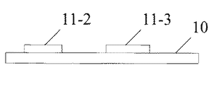
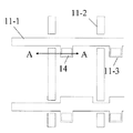
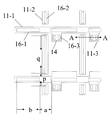
図1A〜図1Jは、本発明の第1の実施形態に係る薄膜トランジスタ(「TFT」)アレイを製造するための方法を示す図である。図1Aは、図1Bに示される平面図のAA方向に沿った断面図である。図1Aによると、例えば、ガラス又は樹脂から作られる基板10が用意される。好ましくは、基板10の厚さは、約0.3〜0.7mm(ミリメートル)の範囲であるが、これより薄くても厚くてもよい。次に、パターニングされた(patterned)第1の金属層11が、例えば、従来の物理的気相成長法(「PVD」)、スパッタリング又は他の好適なプロセスによって基板10上に第1の金属の層を形成し、その次に第1のマスクを使用し従来のパターニング及びエッチングプロセスによって、基板10上に形成される。図1Bによると、パターニングされた第1の金属層11は、互いに実質的に平行な複数の第1の導電性ライン11−1と、第1の導電性ライン11−1に実質的に直交する複数の第2の導電性ライン11−2とを備えている。第1の導電性ライン11−1のそれぞれは、ゲート電極11−3を備えている。それぞれのゲート電極11−3は、1つの第1の導電性ライン11−1と1つの第2の導電性ライン11−2の交点の近くに配置される。第1の金属層のための好適な材料は、TiAlTi、MoAlMo、CrAlCr、MoW、Cr及びCuであるが、これに限定されるものではない。好ましくは、ゲート電極11−3の厚さは、約1000から2000Å(オングストローム)の範囲であるが、他の厚さであってもよい。それぞれの第1の導電性ライン11−1は、最終的に二層配線(dual-layer wire)の主ライン(main line)となり、それぞれの第2の導電性ライン11−2は、最終的に二層配線の分岐ライン(branch line)となる。二層若しくは多層配線構造は、2003年10月20に出願された米国特許出願第10/687759号及び2005年5月17日に出願された米国特許出願第11/131084号に開示され、それらは参照することによりここに組み込まれる。
1A-1J illustrate a method for manufacturing a thin film transistor ("TFT") array according to a first embodiment of the present invention. 1A is a cross-sectional view taken along the direction AA of the plan view shown in FIG. 1B. According to FIG. 1A, for example, a
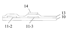
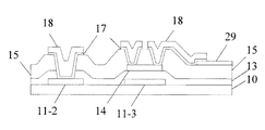
図1C及び図1Dによると、絶縁層13が、例えば従来の化学的気相成長法(「CVD」)プロセス又は他の好適なプロセスによってパターニングされた第1の金属層11上に形成される。絶縁層13のための好適な材料は、窒化ケイ素、酸化ケイ素及び酸窒化ケイ素である。好ましくは、絶縁層13の厚さは、約2500から4000Åの範囲である。次に、パターニングされたシリコン層14が、例えば従来のCVD又は他の好適なプロセスによってシリコンの層を形成し、その次に第2のマスクを使用し従来のパターニング及びエッチングプロセスによって、絶縁層13上に形成される。パターニングされたシリコン層14は、それぞれのゲート電極11−3の上に配置される活性領域を画定する。パターニングされたシリコン層14は、アモルファスシリコン層又は多結晶シリコン層を有している。好ましくは、パターニングされたシリコン層14の厚さは、約500から3000Åの範囲であるが、他の厚さであってもよい。
1C and 1D, an
図1E及び図1Fによると、パターニングされた保護層15が、例えば従来のCVDプロセス又は他の好適なプロセスによって酸化物又は窒化物などの絶縁材料の層を形成し、その次に第3のマスクを使用し従来のパターニング及びエッチングプロセスによって、絶縁層13とパターニングされたシリコン層14の上に形成される。パターニングされた保護層15は、トレンチ(trench)16−1、16−2及び16−3を通じて第1の導電性ライン11−1、第2の導電性ライン11−2及びパターニングされたシリコン層14をそれぞれに露出させる。前記活性領域のそれぞれは、1対のトレンチ16−3を用いて形成され、対応するTFTトランジスタのためのソース領域とドレイン領域を規定する。好ましくは、パターニングされた保護層15の厚さは、約3000から5000Åの範囲である。
According to FIGS. 1E and 1F, the patterned
1つの第1の導電性ライン11−1の上に配置されるそれぞれのトレンチ16−1は、同じ1つの導電性ラインの上に配置される隣接するトレンチ16−1から、“a”として表示される距離だけ離れている。第1の実施形態では、距離“a”に対するトレンチの長さ“b”の比が、約2から20の範囲である。また、1つの第2の導電性ライン11−2の上に配置されるそれぞれのトレンチ16−2は、同じ1つの第2の導電性ライン16−2の上に配置される隣接するトレンチ16−2から、“p”として表示される距離だけ離れている。第1の実施形態では、距離“p”に対するトレンチ16−2の長さ“q”の比が、約2から20の範囲である。 Each trench 16-1 disposed on one first conductive line 11-1 is designated as "a" from an adjacent trench 16-1 disposed on the same one conductive line. It ’s just a distance away. In the first embodiment, the ratio of the trench length “b” to the distance “a” ranges from about 2 to 20. In addition, each trench 16-2 disposed on one second conductive line 11-2 is adjacent to an adjacent trench 16- disposed on the same second conductive line 16-2. 2 away from the distance indicated by “p”. In the first embodiment, the ratio of the length “q” of the trench 16-2 to the distance “p” is in the range of about 2-20.
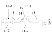
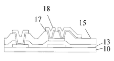
図1G及び図1Hによると、パターニングされたドープシリコン層(doped silicon layer)17とパターニングされた第2の金属層18とが、パターニングされた保護層15の上に形成され、トレンチ16−1、16−2及び16−3を埋める。パターニングされたシリコン層17とパターニングされた第2の金属層18とは、例えば従来のCVDプロセスによって高濃度にドープされたn型(n+)シリコンの層を形成し、その後に、例えば従来のPVDプロセスによって前記n型シリコン層上に第2の金属の層を形成し、その次に第4のマスクを使用し従来のパターニング及びエッチングプロセスによって、形成される。第2の金属層のための好適な材料は、TiAlTi、MoAlMo、CrAlCr、MoW、Cr及びCuであるが、これに限定されるものではない。好ましくは、パターニングされたドープシリコン層17の厚さは、約500Åであるが、それより厚いものでも薄いものでもよい。好ましくは、パターニングされた第2の金属層18の厚さは、約1000から3000Åの範囲である。
According to FIGS. 1G and 1H, a patterned doped
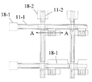
パターニングされた第2の金属層18は、複数の第3の導電性ライン18−1と、第3の導電性ライン18−1に直交する複数の第4の導電性ライン18−2とを備えている。それぞれの第3の導電性ライン18−1は、最終的に二層配線の分岐ラインとなり、それぞれの第4の導電性ライン18−2は、最終的に二層配線の主ラインとなる。パターニングされた第2の金属層18の第3の導電性ライン18−1は、TFTアレイのための二層配線、すなわち二層走査線を形成するために、トレンチ16−1を通じてパターニングされた第1の金属層11の第1の導電性ライン11−1に電気的に接続される。パターニングされた第2の金属層18の第4の導電性ライン18−2は、TFTアレイのための二層配線、すなわち二層データ線を形成するために、トレンチ16−2を通じてパターニングされた第1の金属層11の第2の導電性ライン11−2に電気的に接続される。主ラインに対応する分岐ラインと、同じ前記主ラインに対応する直接隣接する分岐ラインとの間の距離に対する前記主ラインに対応する分岐ラインの長さの比は、約2から20の範囲である。
The patterned
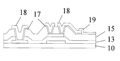
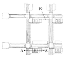
図1I及び図1Jによると、パターニングされた画素電極層19が、従来のPVDプロセスによって、パターニングされた第2の金属層18とパターニングされた保護層15の上に導電性材料、例えばインジウムスズ酸化物(ITO)の層を形成し、その次に第5のマスクを使用し従来のパターニング及びエッチングプロセスによって、形成される。パターニングされた画素電極層19は、TFTアレイのための画素電極としての機能を果たす。好ましくは、前記パターニングされた導電層の厚さは、約500から1000Åの範囲である。
Referring to FIGS. 1I and 1J, the patterned
図2は、本発明の第2の実施形態に係るTFTアレイを製造するための方法を示す断面図である。図2によると、また図1A〜図1Eを参照すると、第1のマスクが、パターニングされた第1の金属層11を規定するために使用される。次に、絶縁材料の層13が、パターニングされた第1の金属層11の上に形成される。第2のマスクが、パターニングされたシリコン層14を規定するために使用される。保護層15が、パターニングされたシリコン層14と絶縁層13の上に形成される。パターニングされた、例えばITO層などの画素電極層29が、従来のPVDプロセスによって、その次に第3のマスクを使用し従来のパターニング及びエッチングプロセスによって、前記保護層上に形成される。その後に、保護層15は、第4のマスクを使用し従来のパターニング及びエッチングプロセスを行うことによってパターニングされ、パターニングされたシリコン層14の一部とパターニングされた第1の金属層11−1と11−2の一部を露出させる。その次に、パターニングされたn型シリコン層17とパターニングされた第2の金属層18とが、第5のマスクを使用しパターニングされた画素電極層29とパターニングされた保護層15の上に形成される。
FIG. 2 is a cross-sectional view showing a method for manufacturing a TFT array according to the second embodiment of the present invention. Referring to FIG. 2 and with reference to FIGS. 1A-1E, a first mask is used to define a patterned first metal layer 11. Next, a
また、図2及び図1A〜図1Eを参照して、第1、第2及び第3のマスクが、パターニングされた第1の金属層11、パターニングされたシリコン層14及びパターニングされた保護層25を規定するためにそれぞれに使用されてもよい。パターニングされた画素電極層29は、従来のPVDプロセスによってITOなどの導電性材料の層を形成し、その次に第4のマスクを使用し従来のパターニング及びエッチングプロセスによって、パターニングされた保護層25の上に形成される。その次に、パターニングされたn型シリコン層17とパターニングされた第2の金属層18とが、第5のマスクを使用しパターニングされた画素電極層29とパターニングされた保護層25の上に形成される。
Also, referring to FIG. 2 and FIGS. 1A to 1E, the first, second, and third masks are patterned first metal layer 11, patterned
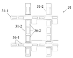
図3は、本発明の第3の実施形態に係るTFTアレイを製造するための方法を示す概略図である。図3によると、パターニングされた第1の金属層31は、複数の第1の導電性ライン31−1と複数の第2の導電性ライン31−2とを備えている。図1Fに示されるトレンチ16−2などのただ1つの連続的なトレンチの代わりに、複数のコンタクトホール36−2が、2つの隣接する第1の導電性ライン31−1の間のそれぞれの第2の導電性ライン31−2に形成されている。また、複数のコンタクトホール36−1が、2つの隣接する第2の導電性ライン31−2の間のそれぞれの第1の導電性ライン31−1に形成されてもよい。
FIG. 3 is a schematic view showing a method for manufacturing a TFT array according to the third embodiment of the present invention. According to FIG. 3, the patterned
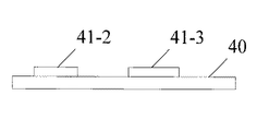
図4A〜図4Jは、本発明の第4の実施形態に係る薄膜トランジスタ(「TFT」)アレイを製造するための方法を示す図である。図4Aは、図4Bに示される平面図のBB方向に沿った断面図である。図4Aによると、例えばガラス又は樹脂から作られる基板40が準備される。パターニングされた第1の金属層41が、従来のPVDプロセスによって基板40上に金属の層を形成し、その次に第1のマスクを使用し従来のパターニング及びエッチングプロセスによって、基板40上に形成される。パターニングされた第1の金属層41は、互いに実質的に平行な複数の第1の導電性ライン41−1と、第1の導電性ライン41−1に実質的に直交する複数の第2の導電性ライン41−2とを備えている。第1の導電性ライン41−1のそれぞれは、ゲート電極41−3を備えている。それぞれのゲート電極41−3は、1つの第1の導電性ライン41−1と1つの第2の導電性ライン41−2の交点の近くに配置される。それぞれの第1の導電性ライン41−1は、最終的に二層配線の主ラインとなり、それぞれの第2の導電性ライン41−2は、最終的に二層配線の分岐ラインとなる。
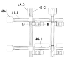
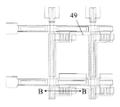
4A-4J are diagrams illustrating a method for manufacturing a thin film transistor ("TFT") array according to a fourth embodiment of the present invention. 4A is a cross-sectional view along the BB direction of the plan view shown in FIG. 4B. According to FIG. 4A, a
図4C及び図4Dによると、絶縁層43が、従来のCVDプロセス又は他の好適なプロセスによってパターニングされた第1の金属層41上に形成されている。次に、パターニングされたシリコン層44が、例えば従来のCVD、レーザアニーリング又は他の好適なプロセスによってシリコンの層を形成し、その次に第2のマスクを使用し従来のパターニング及びエッチングプロセスによって絶縁層43上に形成され、それぞれのゲート電極41−1の上に配置される活性領域を規定する。パターニングされたシリコン層44は、アモルファスシリコン層又は多結晶シリコン層の1つを有している。
4C and 4D, an insulating
図4E及び図4Fによると、パターニングされた保護層45が、従来のCVDプロセスによって絶縁材料の層を形成し、その次に第3のマスクとフォトレジスト層を使用し従来のパターニング及びエッチングプロセスによって、絶縁層43とパターニングされたシリコン層44の上に形成されている。パターニングされた保護層45は、トレンチ46−1、46−2及び46−3を通じて第1の導電性ライン41−1、第2の導電性ライン41−2及びパターニングされたシリコン層44をそれぞれに露出させる。残りのフォトレジスト層42は、例えば従来の注入プロセス又は他の好適なプロセスによってパターニングされたシリコン層44の中へn型又はp型不純物をドープするためのマスクとして使用される。前記フォトレジスト層は、各TFTトランジスタのための第1の拡散領域44−1と第2の拡散領域44−2、すなわちソースとドレイン、又はその逆を規定する。残りのフォトレジスト層42は、その後に取り除かれる。
According to FIGS. 4E and 4F, the patterned
1つの第1の導電性ライン41−1の上に配置されるそれぞれのトレンチ46−1は、同じ1つの導電性ラインの上に配置される隣接するトレンチから距離“a”だけ離れている。第4の実施形態では、距離“a”に対するトレンチの長さ“b”の比が、約2から20の範囲である。また、1つの第2の導電性ライン41−2の上に配置されるそれぞれのトレンチ46−2は、同じ1つの導電性ラインの上に配置される隣接するトレンチから距離“p”だけ離れている。第4の実施形態では、距離“p”に対するトレンチの長さ“q”の比が、約2から20の範囲である。 Each trench 46-1 disposed on one first conductive line 41-1 is separated by a distance "a" from an adjacent trench disposed on the same one conductive line. In the fourth embodiment, the ratio of the trench length “b” to the distance “a” is in the range of about 2-20. In addition, each trench 46-2 disposed on one second conductive line 41-2 is separated from an adjacent trench disposed on the same one conductive line by a distance "p". Yes. In the fourth embodiment, the ratio of the trench length “q” to the distance “p” ranges from about 2 to 20.
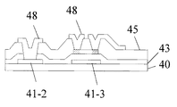
図4G及び図4Hによると、パターニングされた第2の金属層48が、パターニングされた保護層45の上に形成され、トレンチ46−1、46−2及び46−3を埋める。第2の金属層48は、従来のPVDプロセスによって金属の層を形成し、その次に第4のマスクを使用し従来のパターニング及びエッチングプロセスによって、形成される。
According to FIGS. 4G and 4H, a patterned
パターニングされた第2の金属層48は、複数の第3の導電性ライン48−1と、第3の導電性ライン48−1に直交する複数の第4の導電性ライン48−2とを備えている。それぞれの第3の導電性ライン48−1は、最終的に二層配線の分岐ラインとなり、それぞれの第4の導電性ライン48−2は、最終的に二層配線の主ラインとなる。パターニングされた第2の金属層48の第3の導電性ライン48−1は、TFTアレイのための二層配線、すなわち二層走査線を形成するために、トレンチ46−1を通じてパターニングされた第1の金属層11の第1の導電性ライン41−1に電気的に接続される。パターニングされた第2の金属層48の第4の導電性ライン48−2は、TFTアレイのための二層配線、すなわち二層データ線を形成するために、トレンチ46−2を通じてパターニングされた第1の金属層41の第2の導電性ライン41−2に電気的に接続される。主ラインに対応する分岐ラインと、同じ前記主ラインに対応する直接隣接する分岐ラインとの間の距離に対する前記主ラインに対応する分岐ラインの長さの比は、約2から20の範囲である。
The patterned
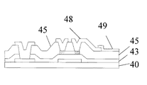
図4I及び図4Jによると、パターニングされた画素電極層49が、従来のPVDプロセスによって、パターニングされた第2の金属層48とパターニングされた保護層45の上にITOなどの導電性材料の層を形成し、その次に第5のマスクを使用し従来のパターニング及びエッチングプロセスによって形成されている。パターニングされた画素電極層49は、TFTアレイのための画素電極としての機能を果たす。
Referring to FIGS. 4I and 4J, the patterned
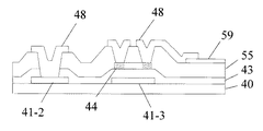
図5は、本発明の第5の実施形態に係るTFTアレイを製造するための方法を示す断面図である。図5によると、また図4A〜図4Eを参照すると、第1のマスクが、パターニングされた第1の金属層41を規定するために使用される。次に、絶縁材料の層43が、パターニングされたシリコン層44の上に形成される。第2のマスクが、パターニングされたシリコン層44を規定するために使用される。保護層55が、パターニングされたシリコン層44と絶縁層43の上に形成される。パターニングされたITO膜などの画素電極層59が、従来のPVDプロセスによって、その次に第3のマスクを使用し従来のパターニング及びエッチングプロセスによって保護層55上に形成され、TFTアレイのための画素電極としての機能を果たす。その後に、保護層55は、第4のマスクを使用し従来のパターニング及びエッチングプロセスを行うことによってパターニングされ、パターニングされたシリコン層44の一部とパターニングされた第1の金属層41−1と41−2の一部を露出させる。次に、パターニングされたシリコン層44が、同じ第4のマスクを使用し従来の注入プロセスによってn型又はp型不純物を用いてドープされる。その次に、パターニングされた第2の金属層48が、第5のマスクを使用しパターニングされた導電層59とパターニングされた保護層55の上に形成される。
FIG. 5 is a cross-sectional view showing a method for manufacturing a TFT array according to the fifth embodiment of the present invention. According to FIG. 5 and with reference to FIGS. 4A-4E, a first mask is used to define a patterned first metal layer 41. Next, a
また、図5及び図4A〜図4Eを参照して、第1、第2及び第3のマスクは、パターニングされた第1の金属層41、パターニングされたシリコン層44及びパターニングされた保護層55を規定するためにそれぞれに使用される。次に、パターニングされたシリコン層44は、同じ第3のマスクを使用し従来の注入プロセスによって、n型又はp型不純物を用いてドープされる。パターニングされた画素電極層59は、従来のPVDプロセスによってITOなどの導電性材料の層を形成し、その次に第4のマスクを使用し従来のパターニング及びエッチングプロセスによって、パターニングされた保護層55の上に形成される。その次に、パターニングされた第2の金属層48が、第5のマスクを使用しパターニングされた画素電極層59とパターニングされた保護層55の上に形成される。
5 and 4A to 4E, the first, second, and third masks include the patterned first metal layer 41, the patterned
その広範な発明概念から逸脱することなく上記実施形態に対する変更が行われ得ることが当業者により認識されるであろう。従って、本発明は開示される特定の実施形態に限定されるものではないが、添付される特許請求の範囲によって規定されるように、本発明の精神及び範囲内での変更に及んでいることを意図するものであることを理解すべきである。 It will be appreciated by those skilled in the art that modifications to the above embodiments can be made without departing from the broad inventive concept. Accordingly, the invention is not limited to the specific embodiments disclosed, but extends to modifications within the spirit and scope of the invention as defined by the appended claims. It should be understood that this is intended.
更に、本発明の代表的な実施形態を記述することで、本明細書は、ステップの特定の順序として本発明の方法及び/又はプロセスを提供している。しかし、その方法又はプロセスが、ここに記述しているステップの特定の順番に依存するものでない限り、その方法又はプロセスは、記述されるステップの特定の順序に限定されるべきものではない。当業者が理解するように、ステップの他の順序が可能であり得る。従って、この明細書に記述されるステップの特定の順番は、特許請求の範囲において限定するものと解釈すべきものではない。加えて、本発明の方法及び/又はプロセスに指向された特許請求の範囲は、記載された順番でステップを行うものに限定されるべきものではなく、当業者は、その順序を変えることができ、また、本発明の精神及び範囲内にあることを容易に理解できる。 Furthermore, by describing representative embodiments of the present invention, this specification provides the method and / or process of the present invention as a specific order of steps. However, the method or process should not be limited to the specific order of steps described, unless the method or process depends on the specific order of steps described herein. Other sequences of steps may be possible, as will be appreciated by those skilled in the art. Therefore, the specific order of the steps described in this specification should not be construed as limiting in the claims. In addition, the claims directed to the method and / or process of the present invention should not be limited to performing the steps in the order described, but can be varied by one of ordinary skill in the art. Moreover, it can be easily understood that it is within the spirit and scope of the present invention.
10、40 基板
11、31、41 第1の金属層
11−1、31−1、41−1、48−1 第1の導電性ライン
11−2、31−2、41−2、48−2 第2の導電性ライン
11−3、41−3 ゲート電極
13、43 絶縁層
14、44 シリコン層
15、45、55 保護層
17 ドープシリコン層
18、48 第2の金属層
18−1、48−1 第3の導電性ライン
18−2、48−2 第4の導電性ライン
19、29、49、59 画素電極層
16−1、16−2、16−3、46−1、46−2、46−3 トレンチ
36−1、36−2 コンタクトホール
10, 40
Claims (30)
基板を用意するステップと、
前記基板上にパターニングされた第1の金属層を形成し、該パターニングされた第1の金属層が、複数の第1の導電性ラインと該第1の導電性ラインに直交して配置される複数の第2の導電性ラインとを有し、前記第1の導電性ラインのそれぞれが、複数のゲート電極を有し、該ゲート電極のそれぞれが、1つの前記第1の導電性ラインと1つの前記第2の導電性ラインの交点の近くに配置されるステップと、
前記パターニングされた第1の金属層の上に絶縁層を形成するステップと、
パターニングされたシリコン層を形成するステップと、
前記パターニングされたシリコン層と前記パターニングされた第1の金属層の上にパターニングされた保護層を形成し、前記パターニングされたシリコン層の一部とそれぞれ1つの前記第1の導電性ライン及びそれぞれ1つの前記第2の導電性ラインの一部とを露出させるステップと、
前記パターニングされた保護層の上にパターニングされたドープシリコン層とパターニングされた第2の金属層とを形成し、前記パターニングされたシリコン層の露出した部分と前記第1の導電性ライン及び前記第2の導電性ラインの露出した部分とを埋め、前記パターニングされた第2の金属層が、複数の第3の導電性ラインと複数の第4の導電性ラインとを有し、前記第3の導電性ラインと前記第4の導電性ラインのそれぞれが、前記複数の第1の導電性ラインの1つと前記複数の第2の導電性ラインの1つにそれぞれに対応するステップと、
を備えていることを特徴とする方法。 A method for manufacturing a thin film transistor ("TFT") array, comprising:
Preparing a substrate;
A patterned first metal layer is formed on the substrate, and the patterned first metal layer is disposed perpendicular to the plurality of first conductive lines and the first conductive lines. A plurality of second conductive lines, each of the first conductive lines has a plurality of gate electrodes, and each of the gate electrodes includes one first conductive line and one of the first conductive lines. Disposed near the intersection of the two second conductive lines;
Forming an insulating layer on the patterned first metal layer;
Forming a patterned silicon layer;
Forming a patterned protective layer on the patterned silicon layer and the patterned first metal layer, a portion of the patterned silicon layer and each of the first conductive lines and Exposing a portion of one of the second conductive lines;
A patterned doped silicon layer and a patterned second metal layer are formed on the patterned protective layer, and the exposed portion of the patterned silicon layer, the first conductive line, and the first conductive layer are formed. The patterned second metal layer has a plurality of third conductive lines and a plurality of fourth conductive lines, and the third conductive line fills the exposed portion of the second conductive lines. A conductive line and a fourth conductive line respectively corresponding to one of the plurality of first conductive lines and one of the plurality of second conductive lines;
A method characterized by comprising:
前記保護層の上にパターニングされた画素電極層を形成するステップと、
前記保護層をパターニングし、前記パターニングされたシリコン層の一部と前記第1の導電性ライン又は第2の導電性ラインの一部とを露出させるステップと、
をさらに備えていることを特徴とする請求項1に記載の方法。 Forming a protective layer on the patterned silicon layer;
Forming a patterned pixel electrode layer on the protective layer;
Patterning the protective layer to expose a portion of the patterned silicon layer and a portion of the first conductive line or second conductive line;
The method of claim 1, further comprising:
前記パターニングされた保護層と前記パターニングされた画素電極層の上に、パターニングされたドープシリコン層とパターニングされた第2の金属層とを形成し、前記パターニングされたドープシリコン層の露出した部分と前記第1の導電性ライン又は第2の導電性ラインの露出した部分とを埋めるステップと、
をさらに備えていることを特徴とする請求項1に記載の方法。 Forming a patterned pixel electrode layer on the patterned protective layer;
Forming a patterned doped silicon layer and a patterned second metal layer on the patterned protective layer and the patterned pixel electrode layer, and exposing an exposed portion of the patterned doped silicon layer; Filling the exposed portion of the first conductive line or the second conductive line;
The method of claim 1, further comprising:
基板を用意するステップと、
前記基板上にパターニングされた第1の金属層を形成し、該パターニングされた第1の金属層が、複数の第1の導電性ラインと該第1の導電性ラインに直交して配置される複数の第2の導電性ラインとを有し、前記第1の導電性ラインのそれぞれが、複数のゲート電極を有し、該ゲート電極のそれぞれが、1つの前記第1の導電性ラインと1つの前記第2の導電性ラインの交点の近くに配置されるステップと、
前記パターニングされた第1の金属層の上に絶縁層を形成するステップと、
パターニングされたシリコン層を形成するステップと、
前記パターニングされたシリコン層と前記パターニングされた第1の金属層の上にパターニングされた保護層を形成し、前記パターニングされたシリコン層の一部と前記第1の導電性ライン及び前記第2の導電性ラインのそれぞれの一部とを露出させるステップと、
前記パターニングされたシリコン層の露出した部分の中へ不純物をドープするステップと、
前記パターニングされた保護層の上にパターニングされた第2の金属層を形成し、前記パターニングされたシリコン層の露出した部分と前記第1の導電性ライン又は第2の導電性ラインの露出した部分とを埋め、前記パターニングされた第2の金属層が、複数の第3の導電性ラインと複数の第4の導電性ラインとを有し、前記第3の導電性ラインと前記第4の導電性ラインのそれぞれが、前記パターニングされた第1の金属層の前記複数の第1の導電性ラインの1つと前記複数の第2の導電性ラインの1つにそれぞれに対応するステップと、
を備えていることを特徴とする方法。 A method for manufacturing a thin film transistor ("TFT") array, comprising:
Preparing a substrate;
A patterned first metal layer is formed on the substrate, and the patterned first metal layer is disposed perpendicular to the plurality of first conductive lines and the first conductive lines. A plurality of second conductive lines, each of the first conductive lines has a plurality of gate electrodes, and each of the gate electrodes includes one first conductive line and one of the first conductive lines. Disposed near the intersection of the two second conductive lines;
Forming an insulating layer on the patterned first metal layer;
Forming a patterned silicon layer;
A patterned protective layer is formed on the patterned silicon layer and the patterned first metal layer, and a part of the patterned silicon layer, the first conductive line, and the second conductive layer are formed. Exposing a portion of each of the conductive lines;
Doping impurities into exposed portions of the patterned silicon layer;
A patterned second metal layer is formed on the patterned protective layer, and the exposed portion of the patterned silicon layer and the exposed portion of the first conductive line or the second conductive line. And the patterned second metal layer has a plurality of third conductive lines and a plurality of fourth conductive lines, and the third conductive lines and the fourth conductive lines. Each of the conductive lines corresponds to one of the plurality of first conductive lines and one of the plurality of second conductive lines of the patterned first metal layer, respectively.
A method characterized by comprising:
前記保護層の上にパターニングされた画素電極層を形成するステップと、
前記保護層をパターニングし、前記パターニングされたシリコン層の一部と前記第1の導電性ライン又は第2の導電性ラインの一部とを露出させるステップと、
をさらに備えていることを特徴とする請求項14に記載の方法。 Forming a protective layer on the patterned silicon layer;
Forming a patterned pixel electrode layer on the protective layer;
Patterning the protective layer to expose a portion of the patterned silicon layer and a portion of the first conductive line or second conductive line;
15. The method of claim 14, further comprising:
前記パターニングされた保護層の上にパターニングされた画素電極層を形成するステップと、
前記パターニングされた保護層と前記パターニングされた画素電極層の上にパターニングされた第2の金属層を形成し、前記パターニングされたシリコン層の露出した部分と前記第1の導電性ライン又は第2の導電性ラインの露出した部分とを埋めるステップと、
をさらに備えていることを特徴とする請求項14に記載の方法。 Doping impurities into exposed portions of the patterned silicon layer;
Forming a patterned pixel electrode layer on the patterned protective layer;
Forming a patterned second metal layer on the patterned protective layer and the patterned pixel electrode layer, and exposing the exposed portion of the patterned silicon layer and the first conductive line or second; Filling the exposed portion of the conductive line of
15. The method of claim 14, further comprising:
基板を用意するステップと、
前記基板上にパターニングされた第1の金属層を形成し、該パターニングされた第1の金属層が、複数の第1の導電性ラインと該第1の導電性ラインに直交して配置される複数の第2の導電性ラインとを有し、前記第2の導電性ラインのそれぞれが、互いに離れている複数の分岐ラインを有するステップと、
前記パターニングされた第1の金属層の上に絶縁層を形成するステップと、
前記絶縁層の上にパターニングされたシリコン層を形成するステップと、
それぞれの前記第1の導電性ラインの一部と前記パターニングされた第1の金属層のそれぞれの前記第2の導電性ラインの分岐ラインを露出させるステップと、
前記パターニングされたシリコン層の上にパターニングされた第2の金属層を形成し、それぞれの前記第1の導電性ラインの露出した部分とそれぞれの前記第2の導電性ラインの露出した部分を埋め、前記パターニングされた第2の金属層が、複数の第3の導電性ラインと複数の第4の導電性ラインとを有し、前記第3の導電性ラインと前記第4の導電性ラインのそれぞれが、前記パターニングされた第1の金属層の前記複数の第1の導電性ラインの1つと前記複数の第2の導電性ラインの1つにそれぞれに対応するステップと、
を備えていることを特徴とする方法。 A method for manufacturing a thin film transistor ("TFT") array, comprising:
Preparing a substrate;
A patterned first metal layer is formed on the substrate, and the patterned first metal layer is disposed perpendicular to the plurality of first conductive lines and the first conductive lines. A plurality of second conductive lines, each of the second conductive lines having a plurality of branch lines separated from each other;
Forming an insulating layer on the patterned first metal layer;
Forming a patterned silicon layer on the insulating layer;
Exposing a portion of each first conductive line and a branch line of each second conductive line of the patterned first metal layer;
Forming a patterned second metal layer on the patterned silicon layer, filling the exposed portion of each of the first conductive lines and the exposed portion of each of the second conductive lines; The patterned second metal layer has a plurality of third conductive lines and a plurality of fourth conductive lines, and the third conductive lines and the fourth conductive lines are formed. Each corresponding to one of the plurality of first conductive lines and one of the plurality of second conductive lines of the patterned first metal layer, respectively.
A method characterized by comprising:
Applications Claiming Priority (1)
| Application Number | Priority Date | Filing Date | Title |
|---|---|---|---|
| US11/369,624 US7638371B2 (en) | 2006-03-07 | 2006-03-07 | Method for manufacturing thin film transistor display array with dual-layer metal line |
Publications (2)
| Publication Number | Publication Date |
|---|---|
| JP2007241237A true JP2007241237A (en) | 2007-09-20 |
| JP4495712B2 JP4495712B2 (en) | 2010-07-07 |
Family
ID=38479454
Family Applications (1)
| Application Number | Title | Priority Date | Filing Date |
|---|---|---|---|
| JP2006294422A Expired - Fee Related JP4495712B2 (en) | 2006-03-07 | 2006-10-30 | Method for manufacturing a thin film transistor display array having a two-layer metal line |
Country Status (4)
| Country | Link |
|---|---|
| US (1) | US7638371B2 (en) |
| JP (1) | JP4495712B2 (en) |
| CN (1) | CN100477171C (en) |
| TW (1) | TWI356458B (en) |
Cited By (4)
| Publication number | Priority date | Publication date | Assignee | Title |
|---|---|---|---|---|
| JP2012244123A (en) * | 2011-05-24 | 2012-12-10 | Semiconductor Energy Lab Co Ltd | Semiconductor device |
| JP2013219348A (en) * | 2012-03-14 | 2013-10-24 | Semiconductor Energy Lab Co Ltd | Semiconductor device |
| WO2016195001A1 (en) * | 2015-06-04 | 2016-12-08 | シャープ株式会社 | Active matrix substrate |
| JP2019003127A (en) * | 2017-06-19 | 2019-01-10 | 株式会社ジャパンディスプレイ | Liquid crystal display |
Families Citing this family (8)
| Publication number | Priority date | Publication date | Assignee | Title |
|---|---|---|---|---|
| KR101682078B1 (en) * | 2010-07-30 | 2016-12-05 | 삼성디스플레이 주식회사 | Manufacturing method of thin film transistor array panel |
| TWI457672B (en) * | 2011-12-23 | 2014-10-21 | Au Optronics Corp | Pixel structure and manufacturing method thereof |
| US9239502B2 (en) * | 2011-12-23 | 2016-01-19 | Au Optronics Corporation | Pixel structure with data line, scan line and gate electrode formed on the same layer and manufacturing method thereof |
| US20140036188A1 (en) * | 2012-08-01 | 2014-02-06 | Cheng-Hung Chen | Liquid Crystal Display Device, Array Substrate and Manufacturing Method Thereof |
| CN102809859B (en) * | 2012-08-01 | 2014-12-31 | 深圳市华星光电技术有限公司 | Liquid crystal display device, array substrate and manufacture method thereof |
| CN104505392A (en) * | 2014-12-29 | 2015-04-08 | 合肥鑫晟光电科技有限公司 | Array substrate, production method of array substrate, repair method of array substrate and display device |
| CN110853531B (en) * | 2019-11-21 | 2021-11-05 | 京东方科技集团股份有限公司 | Driving backboard for display, preparation method thereof and display panel |
| EP4138126A4 (en) * | 2021-07-09 | 2023-07-19 | Changxin Memory Technologies, Inc. | Semiconductor test structure and forming method therefor |
Citations (2)
| Publication number | Priority date | Publication date | Assignee | Title |
|---|---|---|---|---|
| JP2000002884A (en) * | 1998-06-15 | 2000-01-07 | Sharp Corp | Active matrix substrate and manufacture thereof |
| JP2000352940A (en) * | 1999-06-11 | 2000-12-19 | Toshiba Corp | Matrix array substrate |
Family Cites Families (5)
| Publication number | Priority date | Publication date | Assignee | Title |
|---|---|---|---|---|
| FR2605442B1 (en) | 1986-10-17 | 1988-12-09 | Thomson Csf | ELECTROOPTIC VISUALIZATION SCREEN WITH CONTROL TRANSISTORS AND METHOD FOR PRODUCING THE SAME |
| US20020020840A1 (en) * | 2000-03-10 | 2002-02-21 | Setsuo Nakajima | Semiconductor device and manufacturing method thereof |
| KR100684577B1 (en) * | 2000-06-12 | 2007-02-20 | 엘지.필립스 엘시디 주식회사 | Method for fabricating Transflective liquid crystal display device and the same |
| TWI220775B (en) * | 2003-10-03 | 2004-09-01 | Ind Tech Res Inst | Multi-layered complementary wire structure and manufacturing method thereof |
| US7161226B2 (en) | 2003-10-20 | 2007-01-09 | Industrial Technology Research Institute | Multi-layered complementary wire structure and manufacturing method thereof |
-
2006
- 2006-03-07 US US11/369,624 patent/US7638371B2/en not_active Expired - Fee Related
- 2006-08-23 TW TW095131054A patent/TWI356458B/en not_active IP Right Cessation
- 2006-09-29 CN CN200610140665.8A patent/CN100477171C/en not_active Expired - Fee Related
- 2006-10-30 JP JP2006294422A patent/JP4495712B2/en not_active Expired - Fee Related
Patent Citations (2)
| Publication number | Priority date | Publication date | Assignee | Title |
|---|---|---|---|---|
| JP2000002884A (en) * | 1998-06-15 | 2000-01-07 | Sharp Corp | Active matrix substrate and manufacture thereof |
| JP2000352940A (en) * | 1999-06-11 | 2000-12-19 | Toshiba Corp | Matrix array substrate |
Cited By (7)
| Publication number | Priority date | Publication date | Assignee | Title |
|---|---|---|---|---|
| JP2012244123A (en) * | 2011-05-24 | 2012-12-10 | Semiconductor Energy Lab Co Ltd | Semiconductor device |
| US9525023B2 (en) | 2011-05-24 | 2016-12-20 | Semiconductor Energy Laboratory Co., Ltd. | Semiconductor device |
| JP2013219348A (en) * | 2012-03-14 | 2013-10-24 | Semiconductor Energy Lab Co Ltd | Semiconductor device |
| WO2016195001A1 (en) * | 2015-06-04 | 2016-12-08 | シャープ株式会社 | Active matrix substrate |
| US10367009B2 (en) | 2015-06-04 | 2019-07-30 | Sharp Kabushiki Kaisha | Active-matrix substrate |
| JP2019003127A (en) * | 2017-06-19 | 2019-01-10 | 株式会社ジャパンディスプレイ | Liquid crystal display |
| JP7091027B2 (en) | 2017-06-19 | 2022-06-27 | 株式会社ジャパンディスプレイ | Liquid crystal display device |
Also Published As
| Publication number | Publication date |
|---|---|
| TWI356458B (en) | 2012-01-11 |
| TW200735229A (en) | 2007-09-16 |
| CN101034685A (en) | 2007-09-12 |
| JP4495712B2 (en) | 2010-07-07 |
| US20070212824A1 (en) | 2007-09-13 |
| CN100477171C (en) | 2009-04-08 |
| US7638371B2 (en) | 2009-12-29 |
Similar Documents
| Publication | Publication Date | Title |
|---|---|---|
| JP4495712B2 (en) | Method for manufacturing a thin film transistor display array having a two-layer metal line | |
| US7800177B2 (en) | Thin film transistor plate and method of fabricating the same | |
| US7759178B2 (en) | Thin film transistor substrate and fabrication thereof | |
| US7768010B2 (en) | Poly crystalline silicon semiconductor device and method of fabricating the same | |
| US20090224257A1 (en) | Thin film transistor panel and manufacturing method of the same | |
| KR20080012768A (en) | Display device and manufacturing method thereof | |
| US6166785A (en) | Thin film transistor and fabricating method thereof having patterned active layer | |
| JP2007173652A (en) | Thin-film transistor, manufacturing method therefor, and display device having the same | |
| JP2008028399A (en) | Display with thin film transistor device having different electrical characteristics in pixel and driving regions, and method for fabricating the same | |
| JP2007053363A (en) | Interconnect line and its forming method, thin film transistor substrate, and its manufacturing method | |
| JP2007053363A5 (en) | ||
| JP2010199556A (en) | Method of forming multilayered film, method of manufacturing display panel | |
| KR101134989B1 (en) | Method of fabricating array substrate | |
| TW200409364A (en) | Structure of thin film transistor array and driving circuits | |
| JPH11326941A (en) | Active matrix display device | |
| JP2005274984A (en) | Display device and display device manufacturing method | |
| CN111029346A (en) | Display panel, manufacturing method thereof and electronic equipment | |
| KR100580825B1 (en) | Method for fabricating a active matrix substrate and a gate IC pad, thin film transistor fabricated the same | |
| JP5671443B2 (en) | Polycrystalline silicon semiconductor device and manufacturing method thereof | |
| KR20070040017A (en) | Thin film transistor and fabrication method of the same | |
| KR100502813B1 (en) | Manufacturing Method of Thin Film Transistor, Thin Film Transistor Board and Manufacturing Method Thereof | |
| KR101706228B1 (en) | Method of manufacturing of array substrate | |
| KR20060102172A (en) | Thin film transistor array panel | |
| KR100269356B1 (en) | Method of fabricating thin film transistor | |
| KR20060059582A (en) | An array substrate for lcd with two type tft and method of fabrication thereof |
Legal Events
| Date | Code | Title | Description |
|---|---|---|---|
| RD04 | Notification of resignation of power of attorney |
Free format text: JAPANESE INTERMEDIATE CODE: A7424 Effective date: 20090212 |
|
| A131 | Notification of reasons for refusal |
Free format text: JAPANESE INTERMEDIATE CODE: A131 Effective date: 20090825 |
|
| A601 | Written request for extension of time |
Free format text: JAPANESE INTERMEDIATE CODE: A601 Effective date: 20091125 |
|
| A602 | Written permission of extension of time |
Free format text: JAPANESE INTERMEDIATE CODE: A602 Effective date: 20091130 |
|
| A521 | Request for written amendment filed |
Free format text: JAPANESE INTERMEDIATE CODE: A523 Effective date: 20091221 |
|
| TRDD | Decision of grant or rejection written | ||
| A01 | Written decision to grant a patent or to grant a registration (utility model) |
Free format text: JAPANESE INTERMEDIATE CODE: A01 Effective date: 20100323 |
|
| A01 | Written decision to grant a patent or to grant a registration (utility model) |
Free format text: JAPANESE INTERMEDIATE CODE: A01 |
|
| A61 | First payment of annual fees (during grant procedure) |
Free format text: JAPANESE INTERMEDIATE CODE: A61 Effective date: 20100409 |
|
| R150 | Certificate of patent or registration of utility model |
Ref document number: 4495712 Country of ref document: JP Free format text: JAPANESE INTERMEDIATE CODE: R150 Free format text: JAPANESE INTERMEDIATE CODE: R150 |
|
| FPAY | Renewal fee payment (event date is renewal date of database) |
Free format text: PAYMENT UNTIL: 20130416 Year of fee payment: 3 |
|
| FPAY | Renewal fee payment (event date is renewal date of database) |
Free format text: PAYMENT UNTIL: 20130416 Year of fee payment: 3 |
|
| FPAY | Renewal fee payment (event date is renewal date of database) |
Free format text: PAYMENT UNTIL: 20140416 Year of fee payment: 4 |
|
| R250 | Receipt of annual fees |
Free format text: JAPANESE INTERMEDIATE CODE: R250 |
|
| R250 | Receipt of annual fees |
Free format text: JAPANESE INTERMEDIATE CODE: R250 |
|
| R250 | Receipt of annual fees |
Free format text: JAPANESE INTERMEDIATE CODE: R250 |
|
| R250 | Receipt of annual fees |
Free format text: JAPANESE INTERMEDIATE CODE: R250 |
|
| R250 | Receipt of annual fees |
Free format text: JAPANESE INTERMEDIATE CODE: R250 |
|
| R250 | Receipt of annual fees |
Free format text: JAPANESE INTERMEDIATE CODE: R250 |
|
| LAPS | Cancellation because of no payment of annual fees |