JP2007208041A - 半導体装置及び半導体装置の製造方法 - Google Patents
半導体装置及び半導体装置の製造方法 Download PDFInfo
- Publication number
- JP2007208041A JP2007208041A JP2006025649A JP2006025649A JP2007208041A JP 2007208041 A JP2007208041 A JP 2007208041A JP 2006025649 A JP2006025649 A JP 2006025649A JP 2006025649 A JP2006025649 A JP 2006025649A JP 2007208041 A JP2007208041 A JP 2007208041A
- Authority
- JP
- Japan
- Prior art keywords
- light
- emitting element
- semiconductor device
- cover
- light emitting
- Prior art date
- Legal status (The legal status is an assumption and is not a legal conclusion. Google has not performed a legal analysis and makes no representation as to the accuracy of the status listed.)
- Granted
Links
Images


Classifications
-
- H—ELECTRICITY
- H01—ELECTRIC ELEMENTS
- H01L—SEMICONDUCTOR DEVICES NOT COVERED BY CLASS H10
- H01L33/00—Semiconductor devices with at least one potential-jump barrier or surface barrier specially adapted for light emission; Processes or apparatus specially adapted for the manufacture or treatment thereof or of parts thereof; Details thereof
- H01L33/48—Semiconductor devices with at least one potential-jump barrier or surface barrier specially adapted for light emission; Processes or apparatus specially adapted for the manufacture or treatment thereof or of parts thereof; Details thereof characterised by the semiconductor body packages
- H01L33/58—Optical field-shaping elements
-
- H—ELECTRICITY
- H01—ELECTRIC ELEMENTS
- H01L—SEMICONDUCTOR DEVICES NOT COVERED BY CLASS H10
- H01L24/00—Arrangements for connecting or disconnecting semiconductor or solid-state bodies; Methods or apparatus related thereto
- H01L24/93—Batch processes
- H01L24/95—Batch processes at chip-level, i.e. with connecting carried out on a plurality of singulated devices, i.e. on diced chips
- H01L24/97—Batch processes at chip-level, i.e. with connecting carried out on a plurality of singulated devices, i.e. on diced chips the devices being connected to a common substrate, e.g. interposer, said common substrate being separable into individual assemblies after connecting
-
- H—ELECTRICITY
- H01—ELECTRIC ELEMENTS
- H01L—SEMICONDUCTOR DEVICES NOT COVERED BY CLASS H10
- H01L2224/00—Indexing scheme for arrangements for connecting or disconnecting semiconductor or solid-state bodies and methods related thereto as covered by H01L24/00
- H01L2224/01—Means for bonding being attached to, or being formed on, the surface to be connected, e.g. chip-to-package, die-attach, "first-level" interconnects; Manufacturing methods related thereto
- H01L2224/10—Bump connectors; Manufacturing methods related thereto
- H01L2224/12—Structure, shape, material or disposition of the bump connectors prior to the connecting process
- H01L2224/13—Structure, shape, material or disposition of the bump connectors prior to the connecting process of an individual bump connector
-
- H—ELECTRICITY
- H01—ELECTRIC ELEMENTS
- H01L—SEMICONDUCTOR DEVICES NOT COVERED BY CLASS H10
- H01L2224/00—Indexing scheme for arrangements for connecting or disconnecting semiconductor or solid-state bodies and methods related thereto as covered by H01L24/00
- H01L2224/01—Means for bonding being attached to, or being formed on, the surface to be connected, e.g. chip-to-package, die-attach, "first-level" interconnects; Manufacturing methods related thereto
- H01L2224/42—Wire connectors; Manufacturing methods related thereto
- H01L2224/47—Structure, shape, material or disposition of the wire connectors after the connecting process
- H01L2224/48—Structure, shape, material or disposition of the wire connectors after the connecting process of an individual wire connector
- H01L2224/4805—Shape
- H01L2224/4809—Loop shape
- H01L2224/48091—Arched
-
- H—ELECTRICITY
- H01—ELECTRIC ELEMENTS
- H01L—SEMICONDUCTOR DEVICES NOT COVERED BY CLASS H10
- H01L2924/00—Indexing scheme for arrangements or methods for connecting or disconnecting semiconductor or solid-state bodies as covered by H01L24/00
- H01L2924/10—Details of semiconductor or other solid state devices to be connected
- H01L2924/11—Device type
- H01L2924/12—Passive devices, e.g. 2 terminal devices
- H01L2924/1204—Optical Diode
- H01L2924/12041—LED
-
- H—ELECTRICITY
- H01—ELECTRIC ELEMENTS
- H01L—SEMICONDUCTOR DEVICES NOT COVERED BY CLASS H10
- H01L33/00—Semiconductor devices with at least one potential-jump barrier or surface barrier specially adapted for light emission; Processes or apparatus specially adapted for the manufacture or treatment thereof or of parts thereof; Details thereof
- H01L33/44—Semiconductor devices with at least one potential-jump barrier or surface barrier specially adapted for light emission; Processes or apparatus specially adapted for the manufacture or treatment thereof or of parts thereof; Details thereof characterised by the coatings, e.g. passivation layer or anti-reflective coating
-
- H—ELECTRICITY
- H01—ELECTRIC ELEMENTS
- H01L—SEMICONDUCTOR DEVICES NOT COVERED BY CLASS H10
- H01L33/00—Semiconductor devices with at least one potential-jump barrier or surface barrier specially adapted for light emission; Processes or apparatus specially adapted for the manufacture or treatment thereof or of parts thereof; Details thereof
- H01L33/48—Semiconductor devices with at least one potential-jump barrier or surface barrier specially adapted for light emission; Processes or apparatus specially adapted for the manufacture or treatment thereof or of parts thereof; Details thereof characterised by the semiconductor body packages
- H01L33/50—Wavelength conversion elements
- H01L33/507—Wavelength conversion elements the elements being in intimate contact with parts other than the semiconductor body or integrated with parts other than the semiconductor body
-
- H—ELECTRICITY
- H01—ELECTRIC ELEMENTS
- H01L—SEMICONDUCTOR DEVICES NOT COVERED BY CLASS H10
- H01L33/00—Semiconductor devices with at least one potential-jump barrier or surface barrier specially adapted for light emission; Processes or apparatus specially adapted for the manufacture or treatment thereof or of parts thereof; Details thereof
- H01L33/48—Semiconductor devices with at least one potential-jump barrier or surface barrier specially adapted for light emission; Processes or apparatus specially adapted for the manufacture or treatment thereof or of parts thereof; Details thereof characterised by the semiconductor body packages
- H01L33/58—Optical field-shaping elements
- H01L33/60—Reflective elements
Abstract
【解決手段】半導体装置100は、基板101に発光素子102が実装されている。発光素子102は、上面に光の反射を防止する光反射防止膜130が形成されている。そのため、発光素子102の内部から外部に放射された光が発光素子102の上面(屈折率の境界面)を通過して進行する際に、屈折率の差によって光の全反射が起きることが防止される。また、発光素子102上には、光透過性を有するガラスよりなる平板状のカバー103が設置され、当該カバー103の上面にも光の反射を防止する光反射防止膜140が形成されている。そのため、発光素子102からの光がカバー103を透過して屈折率の大きいガラス製のカバー103から屈折率の小さい空気へ進行する過程で全反射することが防止される。
【選択図】図1
Description
Sinθf=n2/n1・・・(1)
この場合、全反射が生じるためには、物質Aの屈折率n1、物質Bの屈折率n2は、次式(2)の条件を満たしていることが必要になる。
n1>n2・・・(2)
従って、サファイア基板の屈折率(=1.8)に対して空気の屈折率(=1.0)が小さいので、発光素子102の内部から外部に放射された光は、境界面に対する入射角が上記臨界角θfより大きい角度である場合には、全反射となり、発光された光が入射角によって発光素子102の外部に進行することができなくなる。
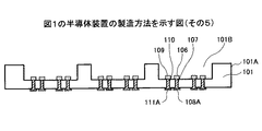
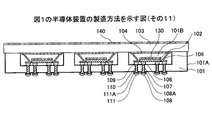
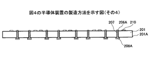
101,201,301 基板
102,202,302 発光素子
103,203,303 カバー
104,204,304 蛍光体膜
105,205 リフレクタ
130,140,230,240,330,340 光反射防止膜
Claims (10)
- 基板に光機能素子が実装されてなる半導体装置であって、
前記光機能素子上には光透過性を有するカバーが設置され、
少なくとも前記カバーまたは前記光機能素子の何れかに光の反射を防止する光反射防止膜が形成されていることを特徴とする半導体装置。 - 前記カバーは、少なくともおもて面及び裏面の何れかに前記光反射防止膜が形成されていることを特徴とする請求項1に記載の半導体装置。
- 前記光反射防止膜は、誘電体膜を多層コーティングして形成された透明膜であることを特徴とする請求項1または2に記載の半導体装置。
- 前記光機能素子は、光を発光する発光素子であり、
前記発光素子の側面を囲むように光を反射するリフレクタが配置されていることを特徴とする請求項1乃至3の何れかに記載の半導体装置。 - 前記光機能素子は、前記基板の凹部に実装され、前記凹部が前記カバーと前記基板が接合されて封止されていることを特徴とする請求項4に記載の半導体装置。
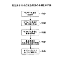
- 基板上に光機能素子を実装する工程と、
前記基板上に設置された前記光機能素子を、光透過性を有するカバーを用いて封止する工程と、
少なくとも前記カバーまたは前記光機能素子の何れかに光反射防止膜を形成する工程と、
を有することを特徴とする半導体装置の製造方法。 - 前記光反射防止膜は、誘電体膜を多層コーティングして形成された透明膜であることを特徴とする請求項6に記載の半導体装置の製造方法。
- 前記基板は、前記光機能素子を実装する凹部が形成され、
前記凹部の開口は、前記カバーを用いて封止されていることを特徴とする請求項6に記載の半導体装置の製造方法。 - 前記光機能素子は、光を発光する発光素子であり、
前記発光素子の側面を囲むように光を反射するリフレクタを配置する工程を有することを特徴とする請求項6に記載の半導体装置の製造方法。 - 前記リフレクタの上端を前記カバーに接合する工程と、
前記リフレクタの下端を前記光機能素子が載置された領域の周囲に接合して前記光機能素子が実装された空間を封止する工程と、
を有することを特徴とする請求項9に記載の半導体装置の製造方法。
Priority Applications (4)
| Application Number | Priority Date | Filing Date | Title |
|---|---|---|---|
| JP2006025649A JP4996101B2 (ja) | 2006-02-02 | 2006-02-02 | 半導体装置及び半導体装置の製造方法 |
| EP07002224A EP1816687A2 (en) | 2006-02-02 | 2007-02-01 | Semiconductor device and method of manufacturing semiconductor device |
| US11/700,761 US7825423B2 (en) | 2006-02-02 | 2007-02-01 | Semiconductor device and method of manufacturing semiconductor device |
| TW096103824A TW200805707A (en) | 2006-02-02 | 2007-02-02 | Semiconductor device and method of manufacturing semiconductor device |
Applications Claiming Priority (1)
| Application Number | Priority Date | Filing Date | Title |
|---|---|---|---|
| JP2006025649A JP4996101B2 (ja) | 2006-02-02 | 2006-02-02 | 半導体装置及び半導体装置の製造方法 |
Publications (3)
| Publication Number | Publication Date |
|---|---|
| JP2007208041A true JP2007208041A (ja) | 2007-08-16 |
| JP2007208041A5 JP2007208041A5 (ja) | 2008-12-25 |
| JP4996101B2 JP4996101B2 (ja) | 2012-08-08 |
Family
ID=38038555
Family Applications (1)
| Application Number | Title | Priority Date | Filing Date |
|---|---|---|---|
| JP2006025649A Expired - Fee Related JP4996101B2 (ja) | 2006-02-02 | 2006-02-02 | 半導体装置及び半導体装置の製造方法 |
Country Status (4)
| Country | Link |
|---|---|
| US (1) | US7825423B2 (ja) |
| EP (1) | EP1816687A2 (ja) |
| JP (1) | JP4996101B2 (ja) |
| TW (1) | TW200805707A (ja) |
Cited By (14)
| Publication number | Priority date | Publication date | Assignee | Title |
|---|---|---|---|---|
| EP2058872A2 (en) | 2007-11-06 | 2009-05-13 | Shinko Electric Industries Co., Ltd. | Semiconductor package |
| JP2009111082A (ja) * | 2007-10-29 | 2009-05-21 | Shinko Electric Ind Co Ltd | パッケージ用シリコン基板 |
| JP2010539715A (ja) * | 2007-09-21 | 2010-12-16 | オスラム オプト セミコンダクターズ ゲゼルシャフト ミット ベシュレンクテル ハフツング | 放射放出コンポーネント |
| KR20120013548A (ko) * | 2010-08-05 | 2012-02-15 | 엘지이노텍 주식회사 | 발광 소자 패키지 |
| WO2012124473A1 (ja) * | 2011-03-15 | 2012-09-20 | 京セラ株式会社 | 発光装置 |
| JP2012227268A (ja) * | 2011-04-18 | 2012-11-15 | Seiko Instruments Inc | ガラス封止型パッケージの製造方法、及び光学デバイス |
| JP2012529185A (ja) * | 2009-06-02 | 2012-11-15 | ブリッジラックス インコーポレイテッド | 屈折要素を有する光源 |
| JP2013004901A (ja) * | 2011-06-21 | 2013-01-07 | Nippon Kasei Chem Co Ltd | Ledデバイス |
| KR20130124719A (ko) * | 2012-05-07 | 2013-11-15 | 삼성전자주식회사 | 발광소자 |
| JP2014027208A (ja) * | 2012-07-30 | 2014-02-06 | Nichia Chem Ind Ltd | 発光装置とその製造方法 |
| JP2015057826A (ja) * | 2013-09-16 | 2015-03-26 | エルジー イノテック カンパニー リミテッド | 発光素子パッケージ |
| JP2021511040A (ja) * | 2018-01-29 | 2021-05-06 | フィリップ・モーリス・プロダクツ・ソシエテ・アノニム | エアロゾル発生システム用照明ユニット |
| WO2023042461A1 (ja) * | 2021-09-14 | 2023-03-23 | ソニーグループ株式会社 | 半導体発光デバイス |
| US11758948B2 (en) | 2018-01-29 | 2023-09-19 | Altria Client Services Llc | Lighting unit for aerosol-generating systems |
Families Citing this family (24)
| Publication number | Priority date | Publication date | Assignee | Title |
|---|---|---|---|---|
| KR100883075B1 (ko) * | 2007-03-02 | 2009-02-10 | 엘지전자 주식회사 | 전계발광소자 |
| EP2048717A1 (en) * | 2007-10-10 | 2009-04-15 | Unity Opto Technology Co., Ltd. | Structure of light-emitting diode |
| JP2010074117A (ja) * | 2007-12-07 | 2010-04-02 | Panasonic Electric Works Co Ltd | 発光装置 |
| KR100998009B1 (ko) * | 2008-03-12 | 2010-12-03 | 삼성엘이디 주식회사 | 발광 다이오드 패키지 및 그 제조 방법 |
| JP5341915B2 (ja) * | 2008-03-28 | 2013-11-13 | パナソニック株式会社 | 樹脂成型品、半導体発光光源、照明装置及び樹脂成型品の製造方法 |
| DE102008025491A1 (de) * | 2008-05-28 | 2009-12-03 | Osram Opto Semiconductors Gmbh | Optoelektronisches Halbleiterbauteil und Leiterplatte |
| US8058669B2 (en) * | 2008-08-28 | 2011-11-15 | Taiwan Semiconductor Manufacturing Company, Ltd. | Light-emitting diode integration scheme |
| JP2010135488A (ja) * | 2008-12-03 | 2010-06-17 | Toshiba Corp | 発光装置及びその製造方法 |
| DE102009005547A1 (de) * | 2009-01-20 | 2010-07-29 | R. Stahl Schaltgeräte GmbH | Gekapselte Leuchtdiodenanordnung |
| KR101064026B1 (ko) * | 2009-02-17 | 2011-09-08 | 엘지이노텍 주식회사 | 발광 디바이스 패키지 및 그 제조방법 |
| JP5327042B2 (ja) * | 2009-03-26 | 2013-10-30 | 豊田合成株式会社 | Ledランプの製造方法 |
| US8624491B2 (en) * | 2010-07-22 | 2014-01-07 | Kyocera Corporation | Light emitting device |
| TW201310126A (zh) * | 2011-08-18 | 2013-03-01 | Hon Hai Prec Ind Co Ltd | 發光裝置 |
| CN103050583A (zh) * | 2011-10-14 | 2013-04-17 | 展晶科技(深圳)有限公司 | 发光二极管的封装方法 |
| DE102013104240B4 (de) | 2013-04-26 | 2015-10-22 | R. Stahl Schaltgeräte GmbH | Explosionsgeschützte Anordnung elektrischer und/oder elektronischer Bauelemente |
| DE102013111374A1 (de) * | 2013-10-15 | 2015-04-16 | R. Stahl Schaltgeräte GmbH | Explosionsgeschützte Anordnung für elektrische und/oder elektronische Bauelemente |
| CN104124324B (zh) * | 2014-08-06 | 2017-03-01 | 华中科技大学 | 一种led封装玻璃及其制备方法和应用 |
| US10681777B2 (en) * | 2016-04-01 | 2020-06-09 | Infineon Technologies Ag | Light emitter devices, optical filter structures and methods for forming light emitter devices and optical filter structures |
| US10347814B2 (en) | 2016-04-01 | 2019-07-09 | Infineon Technologies Ag | MEMS heater or emitter structure for fast heating and cooling cycles |
| US10559723B2 (en) * | 2017-08-25 | 2020-02-11 | Rohm Co., Ltd. | Optical device |
| US11178392B2 (en) * | 2018-09-12 | 2021-11-16 | Apple Inc. | Integrated optical emitters and applications thereof |
| WO2020163139A2 (en) | 2019-02-04 | 2020-08-13 | Apple Inc. | Vertical emitters with integral microlenses |
| JP7239840B2 (ja) | 2020-08-31 | 2023-03-15 | 日亜化学工業株式会社 | 発光装置の製造方法 |
| CN114864796A (zh) * | 2022-07-05 | 2022-08-05 | 至芯半导体(杭州)有限公司 | 一种紫外器件封装结构及制作方法 |
Citations (7)
| Publication number | Priority date | Publication date | Assignee | Title |
|---|---|---|---|---|
| JPS4846288A (ja) * | 1971-10-13 | 1973-07-02 | ||
| JPS62110995U (ja) * | 1985-12-28 | 1987-07-15 | ||
| JPH06350132A (ja) * | 1993-06-08 | 1994-12-22 | Victor Co Of Japan Ltd | 半導体発光素子アレイ |
| JP2003110146A (ja) * | 2001-07-26 | 2003-04-11 | Matsushita Electric Works Ltd | 発光装置 |
| WO2004001862A1 (ja) * | 2002-06-19 | 2003-12-31 | Sanken Electric Co., Ltd. | 半導体発光装置及びその製法並びに半導体発光装置用リフレクタ |
| WO2005106926A2 (en) * | 2004-04-26 | 2005-11-10 | Gelcore Llc | Light emitting diode component |
| WO2006005062A2 (en) * | 2004-06-30 | 2006-01-12 | Cree, Inc. | Chip-scale methods for packaging light emitting devices and chip-scale packaged light emitting devices |
Family Cites Families (11)
| Publication number | Priority date | Publication date | Assignee | Title |
|---|---|---|---|---|
| US6784463B2 (en) * | 1997-06-03 | 2004-08-31 | Lumileds Lighting U.S., Llc | III-Phospide and III-Arsenide flip chip light-emitting devices |
| JP4280050B2 (ja) * | 2002-10-07 | 2009-06-17 | シチズン電子株式会社 | 白色発光装置 |
| KR101280003B1 (ko) * | 2002-12-25 | 2013-07-05 | 도꾸리쯔교세이호징 가가꾸 기쥬쯔 신꼬 기꼬 | 발광소자장치, 수광소자장치, 광학장치, 플루오르화물 결정, 플루오르화물 결정의 제조방법 및 도가니 |
| KR20040092512A (ko) * | 2003-04-24 | 2004-11-04 | (주)그래픽테크노재팬 | 방열 기능을 갖는 반사판이 구비된 반도체 발광장치 |
| EP1484802B1 (en) * | 2003-06-06 | 2018-06-13 | Stanley Electric Co., Ltd. | Optical semiconductor device |
| JP4138586B2 (ja) * | 2003-06-13 | 2008-08-27 | スタンレー電気株式会社 | 光源用ledランプおよびこれを用いた車両用前照灯 |
| US7560820B2 (en) * | 2004-04-15 | 2009-07-14 | Saes Getters S.P.A. | Integrated getter for vacuum or inert gas packaged LEDs |
| DE102005042778A1 (de) * | 2004-09-09 | 2006-04-13 | Toyoda Gosei Co., Ltd., Nishikasugai | Optische Festkörpervorrichtung |
| US7365371B2 (en) * | 2005-08-04 | 2008-04-29 | Cree, Inc. | Packages for semiconductor light emitting devices utilizing dispensed encapsulants |
| US7798678B2 (en) * | 2005-12-30 | 2010-09-21 | 3M Innovative Properties Company | LED with compound encapsulant lens |
| US7521728B2 (en) * | 2006-01-20 | 2009-04-21 | Cree, Inc. | Packages for semiconductor light emitting devices utilizing dispensed reflectors and methods of forming the same |
-
2006
- 2006-02-02 JP JP2006025649A patent/JP4996101B2/ja not_active Expired - Fee Related
-
2007
- 2007-02-01 EP EP07002224A patent/EP1816687A2/en not_active Withdrawn
- 2007-02-01 US US11/700,761 patent/US7825423B2/en not_active Expired - Fee Related
- 2007-02-02 TW TW096103824A patent/TW200805707A/zh unknown
Patent Citations (7)
| Publication number | Priority date | Publication date | Assignee | Title |
|---|---|---|---|---|
| JPS4846288A (ja) * | 1971-10-13 | 1973-07-02 | ||
| JPS62110995U (ja) * | 1985-12-28 | 1987-07-15 | ||
| JPH06350132A (ja) * | 1993-06-08 | 1994-12-22 | Victor Co Of Japan Ltd | 半導体発光素子アレイ |
| JP2003110146A (ja) * | 2001-07-26 | 2003-04-11 | Matsushita Electric Works Ltd | 発光装置 |
| WO2004001862A1 (ja) * | 2002-06-19 | 2003-12-31 | Sanken Electric Co., Ltd. | 半導体発光装置及びその製法並びに半導体発光装置用リフレクタ |
| WO2005106926A2 (en) * | 2004-04-26 | 2005-11-10 | Gelcore Llc | Light emitting diode component |
| WO2006005062A2 (en) * | 2004-06-30 | 2006-01-12 | Cree, Inc. | Chip-scale methods for packaging light emitting devices and chip-scale packaged light emitting devices |
Cited By (21)
| Publication number | Priority date | Publication date | Assignee | Title |
|---|---|---|---|---|
| JP2010539715A (ja) * | 2007-09-21 | 2010-12-16 | オスラム オプト セミコンダクターズ ゲゼルシャフト ミット ベシュレンクテル ハフツング | 放射放出コンポーネント |
| JP2009111082A (ja) * | 2007-10-29 | 2009-05-21 | Shinko Electric Ind Co Ltd | パッケージ用シリコン基板 |
| US7989927B2 (en) | 2007-10-29 | 2011-08-02 | Shinko Electric Industries Co., Ltd. | Silicon substrate for package |
| US8106484B2 (en) | 2007-10-29 | 2012-01-31 | Shinko Electric Industries Co., Ltd. | Silicon substrate for package |
| US7960820B2 (en) | 2007-11-06 | 2011-06-14 | Shinko Electric Industries Co., Ltd. | Semiconductor package |
| EP2058872A2 (en) | 2007-11-06 | 2009-05-13 | Shinko Electric Industries Co., Ltd. | Semiconductor package |
| JP2012529185A (ja) * | 2009-06-02 | 2012-11-15 | ブリッジラックス インコーポレイテッド | 屈折要素を有する光源 |
| KR101714042B1 (ko) * | 2010-08-05 | 2017-03-08 | 엘지이노텍 주식회사 | 발광 소자 패키지 |
| KR20120013548A (ko) * | 2010-08-05 | 2012-02-15 | 엘지이노텍 주식회사 | 발광 소자 패키지 |
| WO2012124473A1 (ja) * | 2011-03-15 | 2012-09-20 | 京セラ株式会社 | 発光装置 |
| JP2012227268A (ja) * | 2011-04-18 | 2012-11-15 | Seiko Instruments Inc | ガラス封止型パッケージの製造方法、及び光学デバイス |
| JP2013004901A (ja) * | 2011-06-21 | 2013-01-07 | Nippon Kasei Chem Co Ltd | Ledデバイス |
| KR20130124719A (ko) * | 2012-05-07 | 2013-11-15 | 삼성전자주식회사 | 발광소자 |
| KR101887942B1 (ko) * | 2012-05-07 | 2018-08-14 | 삼성전자주식회사 | 발광소자 |
| US9324925B2 (en) | 2012-07-30 | 2016-04-26 | Nichia Corporation | Light emitting device having a metal film extending from the first electrode |
| JP2014027208A (ja) * | 2012-07-30 | 2014-02-06 | Nichia Chem Ind Ltd | 発光装置とその製造方法 |
| JP2015057826A (ja) * | 2013-09-16 | 2015-03-26 | エルジー イノテック カンパニー リミテッド | 発光素子パッケージ |
| JP2021511040A (ja) * | 2018-01-29 | 2021-05-06 | フィリップ・モーリス・プロダクツ・ソシエテ・アノニム | エアロゾル発生システム用照明ユニット |
| US11758948B2 (en) | 2018-01-29 | 2023-09-19 | Altria Client Services Llc | Lighting unit for aerosol-generating systems |
| JP7376484B2 (ja) | 2018-01-29 | 2023-11-08 | フィリップ・モーリス・プロダクツ・ソシエテ・アノニム | エアロゾル発生システム用照明ユニット |
| WO2023042461A1 (ja) * | 2021-09-14 | 2023-03-23 | ソニーグループ株式会社 | 半導体発光デバイス |
Also Published As
| Publication number | Publication date |
|---|---|
| JP4996101B2 (ja) | 2012-08-08 |
| EP1816687A2 (en) | 2007-08-08 |
| US7825423B2 (en) | 2010-11-02 |
| US20070194712A1 (en) | 2007-08-23 |
| TW200805707A (en) | 2008-01-16 |
Similar Documents
| Publication | Publication Date | Title |
|---|---|---|
| JP4996101B2 (ja) | 半導体装置及び半導体装置の製造方法 | |
| JP5209177B2 (ja) | 半導体装置および半導体装置の製造方法 | |
| US10998479B2 (en) | Light emitting diode | |
| US8017956B2 (en) | Semiconductor light emitting device | |
| CN111129255B (zh) | 发光二极管 | |
| JP2006253298A (ja) | 半導体発光素子及び半導体発光装置 | |
| JP2009267418A (ja) | 発光装置、これを含むパッケージとシステム、およびその製造方法 | |
| JP2005268323A (ja) | 半導体発光装置 | |
| JP5034342B2 (ja) | 発光装置 | |
| JP2008166661A (ja) | 半導体発光装置 | |
| EP4141972A1 (en) | Unit pixel having light-emitting devices, and display device | |
| KR20190010988A (ko) | 자동차 헤드램프용 발광 다이오드 | |
| KR20180095426A (ko) | 측면 반사층을 갖는 발광 다이오드 | |
| KR20230018371A (ko) | 유닛 픽셀 및 디스플레이 장치 | |
| KR20180059157A (ko) | 복수의 파장변환기를 가지는 발광 다이오드 | |
| JP2010278316A (ja) | 発光装置 | |
| JP2010278151A (ja) | 発光装置 | |
| CN215896431U (zh) | 单元像素及显示器装置 | |
| CN215933632U (zh) | 单元像素及显示装置 | |
| CN116210094A (zh) | 高效率发光元件、包括该发光元件的单元像素及包括该单元像素的显示装置 |
Legal Events
| Date | Code | Title | Description |
|---|---|---|---|
| A521 | Request for written amendment filed |
Free format text: JAPANESE INTERMEDIATE CODE: A523 Effective date: 20081107 |
|
| A621 | Written request for application examination |
Free format text: JAPANESE INTERMEDIATE CODE: A621 Effective date: 20081107 |
|
| A977 | Report on retrieval |
Free format text: JAPANESE INTERMEDIATE CODE: A971007 Effective date: 20110419 |
|
| A131 | Notification of reasons for refusal |
Free format text: JAPANESE INTERMEDIATE CODE: A131 Effective date: 20110510 |
|
| A521 | Request for written amendment filed |
Free format text: JAPANESE INTERMEDIATE CODE: A523 Effective date: 20110623 |
|
| A131 | Notification of reasons for refusal |
Free format text: JAPANESE INTERMEDIATE CODE: A131 Effective date: 20110906 |
|
| A521 | Request for written amendment filed |
Free format text: JAPANESE INTERMEDIATE CODE: A523 Effective date: 20111104 |
|
| TRDD | Decision of grant or rejection written | ||
| A01 | Written decision to grant a patent or to grant a registration (utility model) |
Free format text: JAPANESE INTERMEDIATE CODE: A01 Effective date: 20120508 |
|
| A01 | Written decision to grant a patent or to grant a registration (utility model) |
Free format text: JAPANESE INTERMEDIATE CODE: A01 |
|
| A61 | First payment of annual fees (during grant procedure) |
Free format text: JAPANESE INTERMEDIATE CODE: A61 Effective date: 20120511 |
|
| FPAY | Renewal fee payment (event date is renewal date of database) |
Free format text: PAYMENT UNTIL: 20150518 Year of fee payment: 3 |
|
| R150 | Certificate of patent or registration of utility model |
Ref document number: 4996101 Country of ref document: JP Free format text: JAPANESE INTERMEDIATE CODE: R150 Free format text: JAPANESE INTERMEDIATE CODE: R150 |
|
| LAPS | Cancellation because of no payment of annual fees |