JP2007180077A - 半導体装置 - Google Patents
半導体装置 Download PDFInfo
- Publication number
- JP2007180077A JP2007180077A JP2005373734A JP2005373734A JP2007180077A JP 2007180077 A JP2007180077 A JP 2007180077A JP 2005373734 A JP2005373734 A JP 2005373734A JP 2005373734 A JP2005373734 A JP 2005373734A JP 2007180077 A JP2007180077 A JP 2007180077A
- Authority
- JP
- Japan
- Prior art keywords
- lead
- chip
- semiconductor device
- tab
- semiconductor chip
- Prior art date
- Legal status (The legal status is an assumption and is not a legal conclusion. Google has not performed a legal analysis and makes no representation as to the accuracy of the status listed.)
- Pending
Links
Images


Classifications
-
- H—ELECTRICITY
- H01—ELECTRIC ELEMENTS
- H01L—SEMICONDUCTOR DEVICES NOT COVERED BY CLASS H10
- H01L2224/00—Indexing scheme for arrangements for connecting or disconnecting semiconductor or solid-state bodies and methods related thereto as covered by H01L24/00
- H01L2224/01—Means for bonding being attached to, or being formed on, the surface to be connected, e.g. chip-to-package, die-attach, "first-level" interconnects; Manufacturing methods related thereto
- H01L2224/42—Wire connectors; Manufacturing methods related thereto
- H01L2224/44—Structure, shape, material or disposition of the wire connectors prior to the connecting process
- H01L2224/45—Structure, shape, material or disposition of the wire connectors prior to the connecting process of an individual wire connector
- H01L2224/45001—Core members of the connector
- H01L2224/45099—Material
- H01L2224/451—Material with a principal constituent of the material being a metal or a metalloid, e.g. boron (B), silicon (Si), germanium (Ge), arsenic (As), antimony (Sb), tellurium (Te) and polonium (Po), and alloys thereof
- H01L2224/45138—Material with a principal constituent of the material being a metal or a metalloid, e.g. boron (B), silicon (Si), germanium (Ge), arsenic (As), antimony (Sb), tellurium (Te) and polonium (Po), and alloys thereof the principal constituent melting at a temperature of greater than or equal to 950°C and less than 1550°C
- H01L2224/45144—Gold (Au) as principal constituent
-
- H—ELECTRICITY
- H01—ELECTRIC ELEMENTS
- H01L—SEMICONDUCTOR DEVICES NOT COVERED BY CLASS H10
- H01L2224/00—Indexing scheme for arrangements for connecting or disconnecting semiconductor or solid-state bodies and methods related thereto as covered by H01L24/00
- H01L2224/01—Means for bonding being attached to, or being formed on, the surface to be connected, e.g. chip-to-package, die-attach, "first-level" interconnects; Manufacturing methods related thereto
- H01L2224/42—Wire connectors; Manufacturing methods related thereto
- H01L2224/47—Structure, shape, material or disposition of the wire connectors after the connecting process
- H01L2224/48—Structure, shape, material or disposition of the wire connectors after the connecting process of an individual wire connector
- H01L2224/4805—Shape
- H01L2224/4809—Loop shape
- H01L2224/48091—Arched
-
- H—ELECTRICITY
- H01—ELECTRIC ELEMENTS
- H01L—SEMICONDUCTOR DEVICES NOT COVERED BY CLASS H10
- H01L2224/00—Indexing scheme for arrangements for connecting or disconnecting semiconductor or solid-state bodies and methods related thereto as covered by H01L24/00
- H01L2224/01—Means for bonding being attached to, or being formed on, the surface to be connected, e.g. chip-to-package, die-attach, "first-level" interconnects; Manufacturing methods related thereto
- H01L2224/42—Wire connectors; Manufacturing methods related thereto
- H01L2224/47—Structure, shape, material or disposition of the wire connectors after the connecting process
- H01L2224/48—Structure, shape, material or disposition of the wire connectors after the connecting process of an individual wire connector
- H01L2224/481—Disposition
- H01L2224/48135—Connecting between different semiconductor or solid-state bodies, i.e. chip-to-chip
- H01L2224/48137—Connecting between different semiconductor or solid-state bodies, i.e. chip-to-chip the bodies being arranged next to each other, e.g. on a common substrate
-
- H—ELECTRICITY
- H01—ELECTRIC ELEMENTS
- H01L—SEMICONDUCTOR DEVICES NOT COVERED BY CLASS H10
- H01L2224/00—Indexing scheme for arrangements for connecting or disconnecting semiconductor or solid-state bodies and methods related thereto as covered by H01L24/00
- H01L2224/01—Means for bonding being attached to, or being formed on, the surface to be connected, e.g. chip-to-package, die-attach, "first-level" interconnects; Manufacturing methods related thereto
- H01L2224/42—Wire connectors; Manufacturing methods related thereto
- H01L2224/47—Structure, shape, material or disposition of the wire connectors after the connecting process
- H01L2224/48—Structure, shape, material or disposition of the wire connectors after the connecting process of an individual wire connector
- H01L2224/481—Disposition
- H01L2224/48151—Connecting between a semiconductor or solid-state body and an item not being a semiconductor or solid-state body, e.g. chip-to-substrate, chip-to-passive
- H01L2224/48221—Connecting between a semiconductor or solid-state body and an item not being a semiconductor or solid-state body, e.g. chip-to-substrate, chip-to-passive the body and the item being stacked
- H01L2224/48245—Connecting between a semiconductor or solid-state body and an item not being a semiconductor or solid-state body, e.g. chip-to-substrate, chip-to-passive the body and the item being stacked the item being metallic
- H01L2224/48247—Connecting between a semiconductor or solid-state body and an item not being a semiconductor or solid-state body, e.g. chip-to-substrate, chip-to-passive the body and the item being stacked the item being metallic connecting the wire to a bond pad of the item
-
- H—ELECTRICITY
- H01—ELECTRIC ELEMENTS
- H01L—SEMICONDUCTOR DEVICES NOT COVERED BY CLASS H10
- H01L2224/00—Indexing scheme for arrangements for connecting or disconnecting semiconductor or solid-state bodies and methods related thereto as covered by H01L24/00
- H01L2224/01—Means for bonding being attached to, or being formed on, the surface to be connected, e.g. chip-to-package, die-attach, "first-level" interconnects; Manufacturing methods related thereto
- H01L2224/42—Wire connectors; Manufacturing methods related thereto
- H01L2224/47—Structure, shape, material or disposition of the wire connectors after the connecting process
- H01L2224/49—Structure, shape, material or disposition of the wire connectors after the connecting process of a plurality of wire connectors
- H01L2224/491—Disposition
- H01L2224/4912—Layout
- H01L2224/49171—Fan-out arrangements
Landscapes
- Lead Frames For Integrated Circuits (AREA)
Abstract
【解決手段】マイコンチップ2と、メモリチップ3と、マイコンチップ2及びメモリチップ3と接続するタブ5cと、タブ5cを支持する吊りリード5gと、複数のインナリード5aと、封止体4とを有し、タブ5cの2つのチップ間の領域に第1スリット7が形成され、さらに吊りリード5gの一端部は、各辺の複数のインナリード5aの外側に配置され、かつ封止体4の側面に露出しているものである。さらにマイコンチップ2の第1電源/第1GND用の電極とタブ5cの第1バーリード5dとが第1ワイヤ9aで接続され、かつメモリチップ3の第1電源/第1GND用の電極と第1バーリード5dとが第2ワイヤ9bで接続されており、両チップのGND/電源の電極をバーリードによって共通化してQFP(半導体装置)1の端子数の低減化を図る。
【選択図】図1
Description
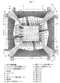
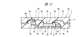
図1は本発明の実施の形態1の半導体装置の内部構造の一例を示す平面図、図2は図1に示すA−A線に沿って切断した構造の一例を示す断面図、図3は図1に示す半導体装置における第1スリットの作用効果の一例を示す概念図、図4及び図5はそれぞれ本発明の実施の形態1の変形例の半導体装置の内部構造を示す平面図、図6〜図13はそれぞれ本発明の実施の形態1の変形例の半導体装置の構造を示す部分断面図である。
図14は本発明の実施の形態2の半導体装置の内部構造の一例を示す平面図、図15は図14に示すA−A線に沿って切断した構造の一例を示す断面図、図16は本発明の実施の形態2の変形例の半導体装置の内部構造を示す平面図、図17は図16に示すA−A線に沿って切断した構造の一例を示す断面図、図18及び図19はそれぞれ本発明の実施の形態2の変形例の半導体装置の内部構造を示す平面図である。
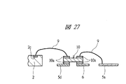
図20は本発明の実施の形態3の半導体装置の内部構造の一例を示す平面図、図21〜図25はそれぞれ本発明の実施の形態3の変形例の半導体装置の内部構造を示す平面図、図26は図25に示す半導体装置におけるチップ部品の実装構造の一例を示す断面図、図27は図25に示す半導体装置におけるチップ部品を介したワイヤ接続状態の変形例を示す部分断面図である。
2 マイコンチップ(第1半導体チップ)
2a 主面
2b 裏面
2c パッド(電極)
3 メモリチップ(第2半導体チップ)
3a 主面
3b 裏面
3c パッド(電極)
4 封止体
4a 表面
4b 裏面
4c 側面
5a インナリード
5b アウタリード
5c タブ
5d 第1バーリード(第1共通リード)
5e 突出部
5f 開口部
5g 吊りリード(第1吊りリード)
5h 端子部
5i 分割部
5j ブリッジ部
5k 分離端子部
6 第2バーリード(第2共通リード)
6a 支持リード(第2吊りリード)
6b 側部
6c 他の支持リード
7 第1スリット
8 第2スリット
9 ワイヤ
9a 第1ワイヤ
9b 第2ワイヤ
9c 第3ワイヤ
9d 第4ワイヤ
9e 第5ワイヤ
9f チップ間ワイヤ(第6ワイヤ)
9g 第7ワイヤ
9h 第8ワイヤ
9i 第9ワイヤ
10 チップコンデンサ(チップ部品)
10a 外部端子
11 抵抗
13 Agペースト
14,15 QFP(半導体装置)
Claims (18)
- 主面に半導体素子及び複数の電極が形成され、かつ演算処理機能を有する第1半導体チップと、
主面に半導体素子及び複数の電極が形成され、かつメモリ回路を有する第2半導体チップと、
前記第1及び第2半導体チップと接続するタブと、
前記タブを支持する吊りリードと、
前記第1半導体チップの周囲に配置された複数のリードと、
前記第1半導体チップの第1電源/第1GND用の電極と前記タブとを電気的に接続する第1ワイヤと、
前記第2半導体チップの第1電源/第1GND用の電極と前記タブとを電気的に接続する第2ワイヤと、
前記第1半導体チップの電極とこれに対応する前記リードとを電気的に接続する第3ワイヤと、
前記第2半導体チップの電極とこれに対応する前記リードとを電気的に接続する第4ワイヤと、
前記第1及び第2半導体チップを封止する封止体とを有し、
前記タブの前記第1半導体チップと前記第2半導体チップの間の領域に第1スリットが形成され、さらに前記吊りリードの一端部は、各辺の前記複数のリードの外側に配置され、かつ前記封止体の側面に露出していることを特徴とする半導体装置。 - 請求項1記載の半導体装置において、前記タブの前記第1ワイヤの接続点と前記第1半導体チップの間の領域に第2スリットが形成されていることを特徴とする半導体装置。
- 請求項1記載の半導体装置において、前記タブ及び前記吊りリードに連結し、かつ前記タブの外周部に配置された第1共通リードと、前記第1共通リードの外側に配置され、かつ前記封止体の側面に露出する支持リードを両端に備え、さらに前記第1半導体チップの第2電源/第2GND用の電極と電気的に接続する第5ワイヤが接続された第2共通リードとを有することを特徴とする半導体装置。
- 請求項3記載の半導体装置において、前記第1共通リードと前記第2共通リードの間にチップ部品が配置されていることを特徴とする半導体装置。
- 請求項3記載の半導体装置において、前記第2共通リードの支持リードは、信号用リードの外側に配置されていることを特徴とする半導体装置。
- 請求項5記載の半導体装置において、前記第2共通リードの長手方向の側部に、前記第
2共通リードに連結する他の支持リードが設けられていることを特徴とする半導体装置。 - 請求項1記載の半導体装置において、前記封止体の裏面側から表面側に向かって、前記第1半導体チップと接続するタブ、前記第2半導体チップと接続する前記タブの突出部、前記リードの順の高さでそれぞれが配置されていることを特徴とする半導体装置。
- 請求項3記載の半導体装置において、前記第1共通リードと前記第2共通リードの間にチップ部品が配置されており、前記封止体の裏面側から表面側に向かって、前記第1半導体チップと接続するタブ、前記第2半導体チップと接続する前記タブの突出部、前記リードの順の高さでそれぞれが配置され、さらに、前記チップ部品を支持する前記第2共通リードは、前記第1半導体チップと接続する前記タブと同じ高さに配置されていることを特徴とする半導体装置。
- 請求項1記載の半導体装置において、前記封止体の裏面側から表面側に向かって、前記第2半導体チップと接続する前記タブの突出部、前記第1半導体チップと接続する前記タブ、前記リードの順の高さでそれぞれが配置されていることを特徴とする半導体装置。
- 請求項1記載の半導体装置において、前記吊りリードの両側に、隣接する前記リード間の隙間より幅広の隙間を有していることを特徴とする半導体装置。
- 請求項3記載の半導体装置において、前記支持リードの両側に、隣接する前記リード間の隙間より幅広の隙間を有していることを特徴とする半導体装置。
- 主面に半導体素子及び複数の電極が形成された半導体チップと、
前記半導体チップの周囲に配置された複数のリードと、
前記半導体チップと接続し、かつ外周部に配置された第1共通リードを有するタブと、
前記第1共通リードの外側に配置され、かつ両端に支持リードを備えた第2共通リードと、
前記半導体チップの第1電源/第1GND用の電極と前記第1共通リードとを電気的に接続する第7ワイヤと、
前記半導体チップの第2電源/第2GND用の電極と前記第2共通リードとを電気的に接続する第8ワイヤと、
前記半導体チップの電極とこれに対応する前記リードとを電気的に接続する第9ワイヤと、
前記タブを支持する吊りリードと、
前記半導体チップを封止する封止体とを有し、
前記吊りリードの少なくとも一部と前記第2共通リードの支持リードが、前記封止体の側面に露出していることを特徴とする半導体装置。 - 請求項12記載の半導体装置において、前記第1共通リードと前記第2共通リードの間にチップ部品が配置されていることを特徴とする半導体装置。
- 請求項12記載の半導体装置において、前記第2共通リードの支持リードは、信号用リードの外側に配置されていることを特徴とする半導体装置。
- 請求項14記載の半導体装置において、前記第2共通リードの長手方向の側部に前記第
2共通リードに連結する他の支持リードが設けられていることを特徴とする半導体装置。 - 請求項12記載の半導体装置において、前記吊りリードの一端部は、各辺の前記複数のリードの外側に配置され、かつ前記封止体の側面に露出していることを特徴とする半導体装置。
- 請求項12記載の半導体装置において、前記第2共通リードの支持リードは、前記リードの内側に配置されていることを特徴とする半導体装置。
- 請求項12記載の半導体装置において、前記吊りリードの先端は、二股に分離していることを特徴とする半導体装置。
Priority Applications (1)
| Application Number | Priority Date | Filing Date | Title |
|---|---|---|---|
| JP2005373734A JP2007180077A (ja) | 2005-12-27 | 2005-12-27 | 半導体装置 |
Applications Claiming Priority (1)
| Application Number | Priority Date | Filing Date | Title |
|---|---|---|---|
| JP2005373734A JP2007180077A (ja) | 2005-12-27 | 2005-12-27 | 半導体装置 |
Publications (2)
| Publication Number | Publication Date |
|---|---|
| JP2007180077A true JP2007180077A (ja) | 2007-07-12 |
| JP2007180077A5 JP2007180077A5 (ja) | 2009-02-12 |
Family
ID=38305004
Family Applications (1)
| Application Number | Title | Priority Date | Filing Date |
|---|---|---|---|
| JP2005373734A Pending JP2007180077A (ja) | 2005-12-27 | 2005-12-27 | 半導体装置 |
Country Status (1)
| Country | Link |
|---|---|
| JP (1) | JP2007180077A (ja) |
Cited By (5)
| Publication number | Priority date | Publication date | Assignee | Title |
|---|---|---|---|---|
| JP2009044114A (ja) * | 2007-07-19 | 2009-02-26 | Renesas Technology Corp | 半導体装置及びその製造方法 |
| JP2010016054A (ja) * | 2008-07-01 | 2010-01-21 | Renesas Technology Corp | 半導体装置およびその製造方法 |
| JP2010186831A (ja) * | 2009-02-10 | 2010-08-26 | Toshiba Corp | 半導体装置 |
| JP2011040573A (ja) * | 2009-08-11 | 2011-02-24 | Renesas Electronics Corp | 半導体装置の製造方法 |
| CN104103534A (zh) * | 2013-04-02 | 2014-10-15 | 瑞萨电子株式会社 | 半导体器件制造方法和半导体器件 |
Citations (2)
| Publication number | Priority date | Publication date | Assignee | Title |
|---|---|---|---|---|
| JPH06252328A (ja) * | 1993-02-23 | 1994-09-09 | Mitsubishi Electric Corp | 半導体素子搭載用のリードフレーム |
| JP2005303222A (ja) * | 2004-04-16 | 2005-10-27 | Renesas Technology Corp | 半導体装置およびその製造方法 |
-
2005
- 2005-12-27 JP JP2005373734A patent/JP2007180077A/ja active Pending
Patent Citations (2)
| Publication number | Priority date | Publication date | Assignee | Title |
|---|---|---|---|---|
| JPH06252328A (ja) * | 1993-02-23 | 1994-09-09 | Mitsubishi Electric Corp | 半導体素子搭載用のリードフレーム |
| JP2005303222A (ja) * | 2004-04-16 | 2005-10-27 | Renesas Technology Corp | 半導体装置およびその製造方法 |
Cited By (11)
| Publication number | Priority date | Publication date | Assignee | Title |
|---|---|---|---|---|
| JP2009044114A (ja) * | 2007-07-19 | 2009-02-26 | Renesas Technology Corp | 半導体装置及びその製造方法 |
| TWI452663B (zh) * | 2007-07-19 | 2014-09-11 | Renesas Electronics Corp | Semiconductor device and manufacturing method thereof |
| TWI514534B (zh) * | 2007-07-19 | 2015-12-21 | Renesas Electronics Corp | Semiconductor device and manufacturing method thereof |
| JP2010016054A (ja) * | 2008-07-01 | 2010-01-21 | Renesas Technology Corp | 半導体装置およびその製造方法 |
| JP2010186831A (ja) * | 2009-02-10 | 2010-08-26 | Toshiba Corp | 半導体装置 |
| KR101121842B1 (ko) * | 2009-02-10 | 2012-03-21 | 가부시끼가이샤 도시바 | 반도체 장치 |
| US8288858B2 (en) | 2009-02-10 | 2012-10-16 | Kabushiki Kaisha Toshiba | Semiconductor device |
| TWI427749B (zh) * | 2009-02-10 | 2014-02-21 | Toshiba Kk | Semiconductor device |
| JP2011040573A (ja) * | 2009-08-11 | 2011-02-24 | Renesas Electronics Corp | 半導体装置の製造方法 |
| CN104103534A (zh) * | 2013-04-02 | 2014-10-15 | 瑞萨电子株式会社 | 半导体器件制造方法和半导体器件 |
| JP2014203879A (ja) * | 2013-04-02 | 2014-10-27 | ルネサスエレクトロニクス株式会社 | 半導体装置の製造方法および半導体装置 |
Similar Documents
| Publication | Publication Date | Title |
|---|---|---|
| US6303997B1 (en) | Thin, stackable semiconductor packages | |
| JP4149438B2 (ja) | 半導体装置 | |
| US7968998B1 (en) | Side leaded, bottom exposed pad and bottom exposed lead fusion quad flat semiconductor package | |
| US5907184A (en) | Integrated circuit package electrical enhancement | |
| JP6164895B2 (ja) | 半導体装置の製造方法 | |
| JP2008532278A (ja) | 付加的な接点パッドを備える集積回路パッケージ装置、リードフレームおよび電子装置 | |
| JP3851845B2 (ja) | 半導体装置 | |
| JP2007180077A (ja) | 半導体装置 | |
| JPH1012658A (ja) | 入出力端子を多数有する半導体集積回路素子 | |
| JP4252563B2 (ja) | 半導体装置 | |
| JPH061801B2 (ja) | リ−ドフレ−ム | |
| JP2018190882A (ja) | 半導体装置 | |
| JPH0399459A (ja) | 樹脂封止型半導体装置 | |
| JPH01143246A (ja) | 半導体装置 | |
| JP2007027645A (ja) | 半導体装置 | |
| KR100635386B1 (ko) | 고속 신호 처리가 가능한 반도체 칩 패키지 | |
| KR100533750B1 (ko) | 반도체 패키지용 리드 프레임 및 이를 이용한 반도체 패키지 | |
| JP2507855B2 (ja) | 半導体装置 | |
| JP2005135938A (ja) | 半導体装置およびその製造方法 | |
| JP2501382B2 (ja) | 半導体装置の組立方法 | |
| JP2002100719A (ja) | 樹脂封止型半導体装置 | |
| JP4153813B2 (ja) | 半導体装置及びその製造方法 | |
| KR100191855B1 (ko) | 센터 패드형 반도체 패키지와 그의 리드 프레임 구조 | |
| KR200164518Y1 (ko) | 반도체 패키지 | |
| JPH0595018A (ja) | 半導体装置の製造方法 |
Legal Events
| Date | Code | Title | Description |
|---|---|---|---|
| A521 | Request for written amendment filed |
Free format text: JAPANESE INTERMEDIATE CODE: A523 Effective date: 20081218 |
|
| A621 | Written request for application examination |
Free format text: JAPANESE INTERMEDIATE CODE: A621 Effective date: 20081218 |
|
| A977 | Report on retrieval |
Free format text: JAPANESE INTERMEDIATE CODE: A971007 Effective date: 20090402 |
|
| A711 | Notification of change in applicant |
Free format text: JAPANESE INTERMEDIATE CODE: A712 Effective date: 20100528 |
|
| A131 | Notification of reasons for refusal |
Free format text: JAPANESE INTERMEDIATE CODE: A131 Effective date: 20110830 |
|
| A02 | Decision of refusal |
Free format text: JAPANESE INTERMEDIATE CODE: A02 Effective date: 20120117 |