JP2005266346A - 基準電圧発生回路、データドライバ、表示装置及び電子機器 - Google Patents
基準電圧発生回路、データドライバ、表示装置及び電子機器 Download PDFInfo
- Publication number
- JP2005266346A JP2005266346A JP2004079051A JP2004079051A JP2005266346A JP 2005266346 A JP2005266346 A JP 2005266346A JP 2004079051 A JP2004079051 A JP 2004079051A JP 2004079051 A JP2004079051 A JP 2004079051A JP 2005266346 A JP2005266346 A JP 2005266346A
- Authority
- JP
- Japan
- Prior art keywords
- data
- component
- circuit
- voltage
- potential side
- Prior art date
- Legal status (The legal status is an assumption and is not a legal conclusion. Google has not performed a legal analysis and makes no representation as to the accuracy of the status listed.)
- Pending
Links
Images


Classifications
-
- G—PHYSICS
- G09—EDUCATION; CRYPTOGRAPHY; DISPLAY; ADVERTISING; SEALS
- G09G—ARRANGEMENTS OR CIRCUITS FOR CONTROL OF INDICATING DEVICES USING STATIC MEANS TO PRESENT VARIABLE INFORMATION
- G09G3/00—Control arrangements or circuits, of interest only in connection with visual indicators other than cathode-ray tubes
- G09G3/20—Control arrangements or circuits, of interest only in connection with visual indicators other than cathode-ray tubes for presentation of an assembly of a number of characters, e.g. a page, by composing the assembly by combination of individual elements arranged in a matrix no fixed position being assigned to or needed to be assigned to the individual characters or partial characters
- G09G3/22—Control arrangements or circuits, of interest only in connection with visual indicators other than cathode-ray tubes for presentation of an assembly of a number of characters, e.g. a page, by composing the assembly by combination of individual elements arranged in a matrix no fixed position being assigned to or needed to be assigned to the individual characters or partial characters using controlled light sources
- G09G3/30—Control arrangements or circuits, of interest only in connection with visual indicators other than cathode-ray tubes for presentation of an assembly of a number of characters, e.g. a page, by composing the assembly by combination of individual elements arranged in a matrix no fixed position being assigned to or needed to be assigned to the individual characters or partial characters using controlled light sources using electroluminescent panels
- G09G3/32—Control arrangements or circuits, of interest only in connection with visual indicators other than cathode-ray tubes for presentation of an assembly of a number of characters, e.g. a page, by composing the assembly by combination of individual elements arranged in a matrix no fixed position being assigned to or needed to be assigned to the individual characters or partial characters using controlled light sources using electroluminescent panels semiconductive, e.g. using light-emitting diodes [LED]
- G09G3/3208—Control arrangements or circuits, of interest only in connection with visual indicators other than cathode-ray tubes for presentation of an assembly of a number of characters, e.g. a page, by composing the assembly by combination of individual elements arranged in a matrix no fixed position being assigned to or needed to be assigned to the individual characters or partial characters using controlled light sources using electroluminescent panels semiconductive, e.g. using light-emitting diodes [LED] organic, e.g. using organic light-emitting diodes [OLED]
- G09G3/3225—Control arrangements or circuits, of interest only in connection with visual indicators other than cathode-ray tubes for presentation of an assembly of a number of characters, e.g. a page, by composing the assembly by combination of individual elements arranged in a matrix no fixed position being assigned to or needed to be assigned to the individual characters or partial characters using controlled light sources using electroluminescent panels semiconductive, e.g. using light-emitting diodes [LED] organic, e.g. using organic light-emitting diodes [OLED] using an active matrix
- G09G3/3233—Control arrangements or circuits, of interest only in connection with visual indicators other than cathode-ray tubes for presentation of an assembly of a number of characters, e.g. a page, by composing the assembly by combination of individual elements arranged in a matrix no fixed position being assigned to or needed to be assigned to the individual characters or partial characters using controlled light sources using electroluminescent panels semiconductive, e.g. using light-emitting diodes [LED] organic, e.g. using organic light-emitting diodes [OLED] using an active matrix with pixel circuitry controlling the current through the light-emitting element
-
- G—PHYSICS
- G09—EDUCATION; CRYPTOGRAPHY; DISPLAY; ADVERTISING; SEALS
- G09G—ARRANGEMENTS OR CIRCUITS FOR CONTROL OF INDICATING DEVICES USING STATIC MEANS TO PRESENT VARIABLE INFORMATION
- G09G3/00—Control arrangements or circuits, of interest only in connection with visual indicators other than cathode-ray tubes
- G09G3/20—Control arrangements or circuits, of interest only in connection with visual indicators other than cathode-ray tubes for presentation of an assembly of a number of characters, e.g. a page, by composing the assembly by combination of individual elements arranged in a matrix no fixed position being assigned to or needed to be assigned to the individual characters or partial characters
- G09G3/22—Control arrangements or circuits, of interest only in connection with visual indicators other than cathode-ray tubes for presentation of an assembly of a number of characters, e.g. a page, by composing the assembly by combination of individual elements arranged in a matrix no fixed position being assigned to or needed to be assigned to the individual characters or partial characters using controlled light sources
- G09G3/30—Control arrangements or circuits, of interest only in connection with visual indicators other than cathode-ray tubes for presentation of an assembly of a number of characters, e.g. a page, by composing the assembly by combination of individual elements arranged in a matrix no fixed position being assigned to or needed to be assigned to the individual characters or partial characters using controlled light sources using electroluminescent panels
- G09G3/32—Control arrangements or circuits, of interest only in connection with visual indicators other than cathode-ray tubes for presentation of an assembly of a number of characters, e.g. a page, by composing the assembly by combination of individual elements arranged in a matrix no fixed position being assigned to or needed to be assigned to the individual characters or partial characters using controlled light sources using electroluminescent panels semiconductive, e.g. using light-emitting diodes [LED]
- G09G3/3208—Control arrangements or circuits, of interest only in connection with visual indicators other than cathode-ray tubes for presentation of an assembly of a number of characters, e.g. a page, by composing the assembly by combination of individual elements arranged in a matrix no fixed position being assigned to or needed to be assigned to the individual characters or partial characters using controlled light sources using electroluminescent panels semiconductive, e.g. using light-emitting diodes [LED] organic, e.g. using organic light-emitting diodes [OLED]
- G09G3/3275—Details of drivers for data electrodes
- G09G3/3291—Details of drivers for data electrodes in which the data driver supplies a variable data voltage for setting the current through, or the voltage across, the light-emitting elements
-
- G—PHYSICS
- G11—INFORMATION STORAGE
- G11C—STATIC STORES
- G11C7/00—Arrangements for writing information into, or reading information out from, a digital store
- G11C7/10—Input/output [I/O] data interface arrangements, e.g. I/O data control circuits, I/O data buffers
- G11C7/1051—Data output circuits, e.g. read-out amplifiers, data output buffers, data output registers, data output level conversion circuits
- G11C7/1057—Data output buffers, e.g. comprising level conversion circuits, circuits for adapting load
-
- G—PHYSICS
- G11—INFORMATION STORAGE
- G11C—STATIC STORES
- G11C7/00—Arrangements for writing information into, or reading information out from, a digital store
- G11C7/10—Input/output [I/O] data interface arrangements, e.g. I/O data control circuits, I/O data buffers
- G11C7/1051—Data output circuits, e.g. read-out amplifiers, data output buffers, data output registers, data output level conversion circuits
- G11C7/106—Data output latches
-
- G—PHYSICS
- G09—EDUCATION; CRYPTOGRAPHY; DISPLAY; ADVERTISING; SEALS
- G09G—ARRANGEMENTS OR CIRCUITS FOR CONTROL OF INDICATING DEVICES USING STATIC MEANS TO PRESENT VARIABLE INFORMATION
- G09G2300/00—Aspects of the constitution of display devices
- G09G2300/08—Active matrix structure, i.e. with use of active elements, inclusive of non-linear two terminal elements, in the pixels together with light emitting or modulating elements
- G09G2300/0809—Several active elements per pixel in active matrix panels
- G09G2300/0842—Several active elements per pixel in active matrix panels forming a memory circuit, e.g. a dynamic memory with one capacitor
-
- G—PHYSICS
- G09—EDUCATION; CRYPTOGRAPHY; DISPLAY; ADVERTISING; SEALS
- G09G—ARRANGEMENTS OR CIRCUITS FOR CONTROL OF INDICATING DEVICES USING STATIC MEANS TO PRESENT VARIABLE INFORMATION
- G09G2310/00—Command of the display device
- G09G2310/02—Addressing, scanning or driving the display screen or processing steps related thereto
- G09G2310/0264—Details of driving circuits
- G09G2310/027—Details of drivers for data electrodes, the drivers handling digital grey scale data, e.g. use of D/A converters
-
- G—PHYSICS
- G09—EDUCATION; CRYPTOGRAPHY; DISPLAY; ADVERTISING; SEALS
- G09G—ARRANGEMENTS OR CIRCUITS FOR CONTROL OF INDICATING DEVICES USING STATIC MEANS TO PRESENT VARIABLE INFORMATION
- G09G2310/00—Command of the display device
- G09G2310/02—Addressing, scanning or driving the display screen or processing steps related thereto
- G09G2310/0264—Details of driving circuits
- G09G2310/0297—Special arrangements with multiplexing or demultiplexing of display data in the drivers for data electrodes, in a pre-processing circuitry delivering display data to said drivers or in the matrix panel, e.g. multiplexing plural data signals to one D/A converter or demultiplexing the D/A converter output to multiple columns
-
- G—PHYSICS
- G09—EDUCATION; CRYPTOGRAPHY; DISPLAY; ADVERTISING; SEALS
- G09G—ARRANGEMENTS OR CIRCUITS FOR CONTROL OF INDICATING DEVICES USING STATIC MEANS TO PRESENT VARIABLE INFORMATION
- G09G2320/00—Control of display operating conditions
- G09G2320/02—Improving the quality of display appearance
- G09G2320/0271—Adjustment of the gradation levels within the range of the gradation scale, e.g. by redistribution or clipping
- G09G2320/0276—Adjustment of the gradation levels within the range of the gradation scale, e.g. by redistribution or clipping for the purpose of adaptation to the characteristics of a display device, i.e. gamma correction
-
- G—PHYSICS
- G09—EDUCATION; CRYPTOGRAPHY; DISPLAY; ADVERTISING; SEALS
- G09G—ARRANGEMENTS OR CIRCUITS FOR CONTROL OF INDICATING DEVICES USING STATIC MEANS TO PRESENT VARIABLE INFORMATION
- G09G2330/00—Aspects of power supply; Aspects of display protection and defect management
- G09G2330/02—Details of power systems and of start or stop of display operation
- G09G2330/021—Power management, e.g. power saving
-
- G—PHYSICS
- G09—EDUCATION; CRYPTOGRAPHY; DISPLAY; ADVERTISING; SEALS
- G09G—ARRANGEMENTS OR CIRCUITS FOR CONTROL OF INDICATING DEVICES USING STATIC MEANS TO PRESENT VARIABLE INFORMATION
- G09G2330/00—Aspects of power supply; Aspects of display protection and defect management
- G09G2330/02—Details of power systems and of start or stop of display operation
- G09G2330/028—Generation of voltages supplied to electrode drivers in a matrix display other than LCD
Abstract
【解決手段】 基準電圧発生回路100は、抵抗回路の両端の電圧を抵抗分割した複数の抵抗分割ノードに複数の基準電圧を出力するガンマ補正抵抗回路110と、抵抗回路の両端に高電位側電圧及び低電位側電圧を供給する高電位側電圧供給回路120及び低電位側電圧供給回路130とを含む。高電位側電圧供給回路120及び低電位側電圧供給回路130は、1画素を構成する色成分ごとに用意された高電位側電圧及び低電位側電圧を、色成分ごとに切り替えて抵抗回路の両端に高電位側電圧及び低電位側電圧を供給する。ガンマ補正抵抗回路110は、電気光学装置のデータ線を駆動する駆動部の入力として選択するための複数の基準電圧信号線に色成分ごとに切り替えられる複数の基準電圧を供給する。
【選択図】 図12
Description
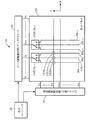
図1に、本実施形態における表示装置の構成例のブロック図を示す。
図4に、図1の走査線駆動回路30の構成例を示す。
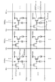
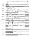
図5に、図1のデータ線駆動回路40の構成例のブロック図を示す。以下では、説明の便宜上、1画素の階調データが18ビット(各色成分の階調データが6ビット)であるものとして説明するが、これに限定されるものではない。
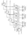
図11に、各色成分の有機EL素子の電圧・輝度特性の一例を示す。図11では、横軸が有機EL素子の印加電圧、縦軸が該有機EL素子の発光輝度であり、色成分ごとに有機EL素子の印加電圧と発光輝度との関係を示している。
本実施形態における表示装置は、電子機器の表示部として搭載される。より具体的には表示装置は、携帯電話機、携帯型情報機器(PDA等)、デジタルカメラ、プロジェクタ、携帯型オーディオプレーヤ、マスストレージデバイス、ビデオカメラ、電子手帳又はGPS(Global Positioning System)などの種々の電子機器に組み込むことができる。
40 データ線駆動回路(データドライバ)、41 シフトレジスタ、
42 データラッチ、43 ラインラッチ、44 多重化回路、
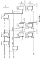
45 DAC(データ電圧生成回路)、46、100 基準電圧発生回路、
47 出力バッファ、50 表示コントローラ、110 ガンマ補正抵抗回路、
120 高電位側電圧供給回路、130 低電位側電圧供給回路、140 セレクタ、
150−R R成分用ガンマ補正設定レジスタ、
150−G G成分用ガンマ補正設定レジスタ、
150−B B成分用ガンマ補正設定レジスタ、
160 ガンマ補正制御回路、V0〜V63 基準電圧、VH 高電位側電圧、
VL 低電位側電圧、Bsel B成分選択信号、BSL、BSL+1 B成分データ線、
c1−1〜c1−4、・・・、c63−1〜c63−4 補正スイッチ制御信号、
c1−1R〜c1−4R、・・・、c63−1R〜c63−4R R成分用の補正スイッチ制御信号、
c1−1G〜c1−4G、・・・、c63−1G〜c63−4G G成分用の補正スイッチ制御信号、
c1−1B〜c1−4B、・・・、c63−1B〜c63−4B B成分用の補正スイッチ制御信号、
DERKL、DEGKL、DEBKL 画素、
DMUX1〜DMUXN、DMUXL、DMUXL+1 デマルチプレクサ、
Gsel G成分選択信号、GSL、GSL+1 G成分データ線、
Rsel R成分選択信号、RSL、RSL+1 R成分データ線、
S1〜SN、SL、SL+1 データ線、G1〜GM、GK、GK+1 走査線
Claims (14)
- 階調データに対応して選択される基準電圧を含む複数の基準電圧を発生するための基準電圧発生回路であって、
抵抗回路を有し、該抵抗回路の両端の電圧を抵抗分割した複数の抵抗分割ノードに複数の基準電圧を出力するガンマ補正抵抗回路と、
前記抵抗回路の両端に、高電位側電圧及び低電位側電圧を供給する第1及び第2の電圧供給回路とを含み、
前記第1及び第2の電圧供給回路が、
1画素を構成する色成分ごとに用意された高電位側電圧及び低電位側電圧の少なくとも1つを、色成分ごとに切り替えて前記抵抗回路の両端に前記高電位側電圧及び低電位側電圧を供給し、
前記ガンマ補正抵抗回路が、
電気光学装置の第1及び第2のデータ線を駆動する第1及び第2の駆動部の入力として選択するための複数の基準電圧信号線の各基準電圧信号線に、色成分ごとに切り替えられる複数の基準電圧の各基準電圧を供給することを特徴とする基準電圧発生回路。 - 請求項1において、
前記ガンマ補正抵抗回路が、
前記複数の抵抗分割ノードのうちいずれか2つの抵抗分割ノード間に挿入された補正スイッチ回路を含み、
前記補正スイッチ回路が、
直列に接続された抵抗素子とスイッチ素子とを有し、該補正スイッチ回路が挿入された前記抵抗分割ノード間を電気的に接続又は遮断することを特徴とする基準電圧発生回路。 - 請求項1又は2において、
前記ガンマ補正抵抗回路が、
複数の基準電圧のうち少なくとも1つの基準電圧を、色成分ごとに異ならせることを特徴とする基準電圧発生回路。 - 請求項1乃至3のいずれかにおいて、
1画素を構成する色成分が、
R成分、G成分及びB成分であり、
R成分の高電位側電圧及び低電位側電圧の差がG成分の高電位側電圧及び低電位側電圧の差より大きく、かつG成分の高電位側電圧及び低電位側電圧の差がB成分の高電位側電圧及び低電位側電圧の差より大きいことを特徴とする基準電圧発生回路。 - 請求項1乃至4のいずれかにおいて、
1画素を構成する色成分が、
R成分、G成分及びB成分であり、
前記高電位側電圧は、
R成分の高電位側電圧、G成分の高電位側電圧及びB成分の高電位側電圧のうち、B成分の高電位側電圧が最も低いことを特徴とする基準電圧発生回路。 - 請求項1乃至5のいずれかにおいて、
前記第1の電圧供給回路が、
ボルテージフォロワ接続された演算増幅器を含み、
該演算増幅器は、pチャネル型駆動トランジスタによりその出力が駆動されることを特徴とする基準電圧発生回路。 - 請求項1乃至6のいずれかにおいて、
前記第2の電圧供給回路が、
ボルテージフォロワ接続された演算増幅器を含み、
該演算増幅器は、nチャネル型駆動トランジスタによりその出力が駆動されることを特徴とする基準電圧発生回路。 - 請求項1乃至7のいずれかにおいて、
前記階調データが、
1画素を構成する色成分ごとに時分割により多重化されており、
前記第1及び第2の電圧供給回路が、
前記階調データの各色成分の時分割タイミングごとに、各色成分の高電位側電圧及び低電位側電圧の少なくとも1つを切り替えて前記抵抗回路の両端に供給することを特徴とする基準電圧発生回路。 - 複数の走査線及び複数のデータ線を含む電気光学装置の前記複数のデータ線を階調データに基づいて駆動するためのデータドライバであって、
請求項1乃至8のいずれか記載の基準電圧発生回路と、
前記複数の基準電圧のうち、第1及び第2の階調データに対応した基準電圧を第1及び第2のデータ電圧として出力するデータ電圧生成回路と、
前記第1のデータ電圧に基づいて前記第1のデータ線を駆動する第1の駆動部と、
前記第2のデータ電圧に基づいて前記第2のデータ線を駆動する第2の駆動部とを含むことを特徴とするデータドライバ。 - 複数の走査線及び複数のデータ線を含む電気光学装置の前記複数のデータ線を階調データに基づいて駆動するためのデータドライバであって、
請求項8記載の基準電圧発生回路と、
1画素の各色成分の階調データを時分割して多重化する多重化回路と、
前記複数の基準電圧のうち、前記多重化回路によって多重化された第1及び第2の階調データに対応した基準電圧を第1及び第2のデータ電圧として出力するデータ電圧生成回路と、
前記第1のデータ電圧に基づいて前記第1のデータ線を駆動する第1の駆動部と、
前記第2のデータ電圧に基づいて前記第2のデータ線を駆動する第2の駆動部とを含むことを特徴とするデータドライバ。 - 複数の走査線と、
複数のデータ線と、
前記複数の走査線及び前記複数のデータ線によって特定される複数の画素と、
前記複数の走査線を走査する走査ドライバと、
前記複数のデータ線を駆動する請求項9又は10記載のデータドライバとを含むことを特徴とする表示装置。 - 複数の走査線と、
複数のデータ線と、
各色成分データ線が1画素を構成する色成分ごとに設けられた複数の色成分データ線と、
前記複数の走査線及び前記複数の色成分データ線によって特定される複数の画素と、
前記複数の走査線を走査する走査ドライバと、
前記複数のデータ線を駆動する請求項10記載のデータドライバと、
各デマルチプレクサがデータ線ごとに設けられ、各デマルチプレクサが各データ線と該各データ線に対応する複数の色成分データ線のいずれかとを前記階調データの時分割タイミングに同期して電気的に接続する複数のデマルチプレクサとを含むことを特徴とする表示装置。 - 請求項11又は12において、
前記複数の画素の各画素が、
エレクトロルミネセンス素子を含むことを特徴とする表示装置。 - 請求項10乃至13のいずれか記載の表示装置を含むことを特徴とする電子機器。
Priority Applications (4)
| Application Number | Priority Date | Filing Date | Title |
|---|---|---|---|
| JP2004079051A JP2005266346A (ja) | 2004-03-18 | 2004-03-18 | 基準電圧発生回路、データドライバ、表示装置及び電子機器 |
| US11/065,773 US7375705B2 (en) | 2004-03-18 | 2005-02-25 | Reference voltage generation circuit, data driver, display device, and electronic instrument |
| CNB2005100557266A CN100442339C (zh) | 2004-03-18 | 2005-03-18 | 基准电压生成电路、数据驱动器、显示装置及电子设备 |
| US12/098,809 US20110057958A1 (en) | 2004-03-18 | 2008-04-07 | Reference voltage generation circuit, data driver, display device, and electronic instrument |
Applications Claiming Priority (1)
| Application Number | Priority Date | Filing Date | Title |
|---|---|---|---|
| JP2004079051A JP2005266346A (ja) | 2004-03-18 | 2004-03-18 | 基準電圧発生回路、データドライバ、表示装置及び電子機器 |
Related Child Applications (1)
| Application Number | Title | Priority Date | Filing Date |
|---|---|---|---|
| JP2011278565A Division JP2012093778A (ja) | 2011-12-20 | 2011-12-20 | 基準電圧発生回路、データドライバ、表示装置及び電子機器 |
Publications (2)
| Publication Number | Publication Date |
|---|---|
| JP2005266346A true JP2005266346A (ja) | 2005-09-29 |
| JP2005266346A5 JP2005266346A5 (ja) | 2008-08-14 |
Family
ID=34986108
Family Applications (1)
| Application Number | Title | Priority Date | Filing Date |
|---|---|---|---|
| JP2004079051A Pending JP2005266346A (ja) | 2004-03-18 | 2004-03-18 | 基準電圧発生回路、データドライバ、表示装置及び電子機器 |
Country Status (3)
| Country | Link |
|---|---|
| US (2) | US7375705B2 (ja) |
| JP (1) | JP2005266346A (ja) |
| CN (1) | CN100442339C (ja) |
Cited By (8)
| Publication number | Priority date | Publication date | Assignee | Title |
|---|---|---|---|---|
| JP2007206589A (ja) * | 2006-02-06 | 2007-08-16 | Seiko Epson Corp | 表示装置、画素回路およびその駆動方法、ならびに電子機器 |
| JP2007274198A (ja) * | 2006-03-30 | 2007-10-18 | Kyocera Corp | 有機el表示装置および有機el表示装置の駆動方法 |
| JP2009180765A (ja) * | 2008-01-29 | 2009-08-13 | Casio Comput Co Ltd | 表示駆動装置、表示装置及びその駆動方法 |
| JP2010128315A (ja) * | 2008-11-28 | 2010-06-10 | Kyocera Corp | 信号処理装置及び画像表示装置 |
| US8368672B2 (en) | 2006-11-16 | 2013-02-05 | Seiko Epson Corporation | Source driver, electro-optical device, and electronic instrument |
| JP2013516655A (ja) * | 2010-01-05 | 2013-05-13 | スリーエム イノベイティブ プロパティズ カンパニー | 色順次画像表示のための光源の制御 |
| JP2015052789A (ja) * | 2008-11-07 | 2015-03-19 | 株式会社半導体エネルギー研究所 | 表示装置 |
| JP2017169196A (ja) * | 2016-03-09 | 2017-09-21 | 株式会社半導体エネルギー研究所 | 半導体装置、表示装置、および電子機器 |
Families Citing this family (27)
| Publication number | Priority date | Publication date | Assignee | Title |
|---|---|---|---|---|
| JP4093231B2 (ja) * | 2004-12-21 | 2008-06-04 | セイコーエプソン株式会社 | 電源回路、表示ドライバ、電気光学装置、電子機器及び電源回路の制御方法 |
| KR100666646B1 (ko) * | 2005-09-15 | 2007-01-09 | 삼성에스디아이 주식회사 | 유기전계발광표시장치 및 유기전계발광표시장치의 구동방법 |
| TW200731199A (en) * | 2006-01-11 | 2007-08-16 | Seiko Epson Corp | Electro-optical device, method of driving electro-optical device, and electronic apparatus |
| KR100965022B1 (ko) * | 2006-02-20 | 2010-06-21 | 도시바 모바일 디스플레이 가부시키가이샤 | El 표시 장치 및 el 표시 장치의 구동 방법 |
| KR101282189B1 (ko) * | 2006-09-13 | 2013-07-05 | 삼성디스플레이 주식회사 | 전압발생회로 및 이를 갖는 표시장치 |
| JP5182781B2 (ja) * | 2006-10-26 | 2013-04-17 | ルネサスエレクトロニクス株式会社 | 表示装置及びデータドライバ |
| KR100815754B1 (ko) * | 2006-11-09 | 2008-03-20 | 삼성에스디아이 주식회사 | 구동회로 및 이를 이용한 유기전계발광표시장치 |
| KR100836437B1 (ko) * | 2006-11-09 | 2008-06-09 | 삼성에스디아이 주식회사 | 데이터구동부 및 그를 이용한 유기전계발광표시장치 |
| KR100911976B1 (ko) | 2007-11-23 | 2009-08-13 | 삼성모바일디스플레이주식회사 | 유기전계발광 표시장치 |
| KR100902245B1 (ko) * | 2008-01-18 | 2009-06-11 | 삼성모바일디스플레이주식회사 | 유기전계발광 표시장치 및 그의 구동방법 |
| JP2010281888A (ja) * | 2009-06-02 | 2010-12-16 | Seiko Epson Corp | 集積回路装置、電気光学装置及び電子機器 |
| TWI436327B (zh) | 2011-03-03 | 2014-05-01 | Novatek Microelectronics Corp | 顯示器之驅動裝置及驅動方法 |
| CN102682723B (zh) * | 2011-03-11 | 2015-11-18 | 联咏科技股份有限公司 | 显示器的驱动装置及驱动方法 |
| TWI448709B (zh) * | 2012-05-15 | 2014-08-11 | Elan Microelectronics Corp | 以不同電壓刺激訊號進行觸控面板優劣檢測方法及其檢測裝置 |
| CN103888560A (zh) * | 2012-12-24 | 2014-06-25 | 鸿富锦精密工业(武汉)有限公司 | 手机保护壳及具有该保护壳的手机 |
| JP5961125B2 (ja) | 2013-02-26 | 2016-08-02 | 株式会社ジャパンディスプレイ | 表示装置及び電子機器 |
| JP5910543B2 (ja) * | 2013-03-06 | 2016-04-27 | ソニー株式会社 | 表示装置、表示駆動回路、表示駆動方法、および電子機器 |
| US10147360B2 (en) * | 2015-03-31 | 2018-12-04 | Universal Display Corporation | Rugged display device architecture |
| JP2016224242A (ja) * | 2015-05-29 | 2016-12-28 | 株式会社ジャパンディスプレイ | 表示装置 |
| KR20170005238A (ko) * | 2015-07-01 | 2017-01-12 | 삼성디스플레이 주식회사 | 데이터 구동 회로, 이를 포함하는 표시 장치 및 이 표시 장치의 구동 방법 |
| KR20170014953A (ko) * | 2015-07-31 | 2017-02-08 | 에스케이하이닉스 주식회사 | 전압 생성 회로 |
| KR20170124684A (ko) * | 2016-05-02 | 2017-11-13 | 삼성디스플레이 주식회사 | 표시장치 및 그의 구동방법 |
| CN105869581B (zh) * | 2016-06-17 | 2019-07-05 | 武汉华星光电技术有限公司 | 液晶显示器驱动电路及液晶显示装置 |
| CN109378024B (zh) * | 2018-11-21 | 2023-09-05 | 灿芯半导体(上海)股份有限公司 | 一种多模式的onfi接口写通道发送电路 |
| CN111435588B (zh) * | 2019-01-15 | 2022-05-13 | 深圳通锐微电子技术有限公司 | 驱动电路及显示装置 |
| CN110379383B (zh) | 2019-06-10 | 2021-05-04 | 惠科股份有限公司 | 参考电压产生电路及显示装置 |
| CN111415617B (zh) * | 2020-04-02 | 2021-07-06 | 广东晟合微电子有限公司 | 增加锁存器提高oled面板伽马电压稳定时间的方法 |
Citations (10)
| Publication number | Priority date | Publication date | Assignee | Title |
|---|---|---|---|---|
| JP2002290172A (ja) * | 2001-03-28 | 2002-10-04 | Sharp Corp | ボルテージフォロア回路および表示装置用駆動装置 |
| JP2002366112A (ja) * | 2001-06-07 | 2002-12-20 | Hitachi Ltd | 液晶駆動装置及び液晶表示装置 |
| JP2003076334A (ja) * | 2001-09-04 | 2003-03-14 | Toshiba Corp | 表示装置 |
| JP2003098998A (ja) * | 2001-09-25 | 2003-04-04 | Toshiba Corp | 平面表示装置 |
| JP2003228332A (ja) * | 2002-02-06 | 2003-08-15 | Toshiba Corp | 表示装置 |
| JP2003233354A (ja) * | 2002-02-08 | 2003-08-22 | Seiko Epson Corp | 基準電圧発生回路、表示駆動回路、表示装置及び基準電圧発生方法 |
| JP2003255900A (ja) * | 2002-02-27 | 2003-09-10 | Sanyo Electric Co Ltd | カラー有機el表示装置 |
| JP2004053715A (ja) * | 2002-07-17 | 2004-02-19 | Sanyo Electric Co Ltd | 表示装置とそのγ補正方法 |
| US20040036706A1 (en) * | 2002-08-26 | 2004-02-26 | Shinji Endou | Display panel driver |
| JP2004354625A (ja) * | 2003-05-28 | 2004-12-16 | Renesas Technology Corp | 自発光表示装置及び自発光表示用駆動回路 |
Family Cites Families (13)
| Publication number | Priority date | Publication date | Assignee | Title |
|---|---|---|---|---|
| JPH11504361A (ja) | 1995-04-25 | 1999-04-20 | ライオンデル ペトロケミカル カンパニー | オレフィンの重合の触媒としてのアザボロリニル金属錯体 |
| US5867057A (en) | 1996-02-02 | 1999-02-02 | United Microelectronics Corp. | Apparatus and method for generating bias voltages for liquid crystal display |
| JPH11175027A (ja) * | 1997-12-08 | 1999-07-02 | Hitachi Ltd | 液晶駆動回路および液晶表示装置 |
| JP2001013478A (ja) * | 1999-06-28 | 2001-01-19 | Fujitsu Ltd | 液晶表示装置用ソース・ドライバ及びそれを用いた液晶表示装置 |
| JP2001195031A (ja) * | 1999-10-27 | 2001-07-19 | Internatl Business Mach Corp <Ibm> | ガンマ補正用基準電位発生回路 |
| JP5008223B2 (ja) | 2000-01-31 | 2012-08-22 | 株式会社半導体エネルギー研究所 | アクティブマトリクス型表示装置 |
| KR100419090B1 (ko) * | 2001-02-19 | 2004-02-19 | 삼성전자주식회사 | 시야각에 적응하는 액정 표시 장치 |
| CN1185787C (zh) * | 2001-04-28 | 2005-01-19 | 凌阳科技股份有限公司 | 可切换电压跟随器及使用该跟随器的桥式驱动电路装置 |
| US6836232B2 (en) * | 2001-12-31 | 2004-12-28 | Himax Technologies, Inc. | Apparatus and method for gamma correction in a liquid crystal display |
| JP3661651B2 (ja) | 2002-02-08 | 2005-06-15 | セイコーエプソン株式会社 | 基準電圧発生回路、表示駆動回路及び表示装置 |
| JP3807321B2 (ja) | 2002-02-08 | 2006-08-09 | セイコーエプソン株式会社 | 基準電圧発生回路、表示駆動回路、表示装置及び基準電圧発生方法 |
| JP3758039B2 (ja) | 2002-06-10 | 2006-03-22 | セイコーエプソン株式会社 | 駆動回路及び電気光学装置 |
| JP2004111262A (ja) * | 2002-09-19 | 2004-04-08 | Nec Yamagata Ltd | ガンマ補正回路およびガンマ補正回路を備えたパネル駆動装置 |
-
2004
- 2004-03-18 JP JP2004079051A patent/JP2005266346A/ja active Pending
-
2005
- 2005-02-25 US US11/065,773 patent/US7375705B2/en not_active Expired - Fee Related
- 2005-03-18 CN CNB2005100557266A patent/CN100442339C/zh not_active Expired - Fee Related
-
2008
- 2008-04-07 US US12/098,809 patent/US20110057958A1/en not_active Abandoned
Patent Citations (11)
| Publication number | Priority date | Publication date | Assignee | Title |
|---|---|---|---|---|
| JP2002290172A (ja) * | 2001-03-28 | 2002-10-04 | Sharp Corp | ボルテージフォロア回路および表示装置用駆動装置 |
| JP2002366112A (ja) * | 2001-06-07 | 2002-12-20 | Hitachi Ltd | 液晶駆動装置及び液晶表示装置 |
| JP2003076334A (ja) * | 2001-09-04 | 2003-03-14 | Toshiba Corp | 表示装置 |
| JP2003098998A (ja) * | 2001-09-25 | 2003-04-04 | Toshiba Corp | 平面表示装置 |
| JP2003228332A (ja) * | 2002-02-06 | 2003-08-15 | Toshiba Corp | 表示装置 |
| JP2003233354A (ja) * | 2002-02-08 | 2003-08-22 | Seiko Epson Corp | 基準電圧発生回路、表示駆動回路、表示装置及び基準電圧発生方法 |
| JP2003255900A (ja) * | 2002-02-27 | 2003-09-10 | Sanyo Electric Co Ltd | カラー有機el表示装置 |
| JP2004053715A (ja) * | 2002-07-17 | 2004-02-19 | Sanyo Electric Co Ltd | 表示装置とそのγ補正方法 |
| US20040036706A1 (en) * | 2002-08-26 | 2004-02-26 | Shinji Endou | Display panel driver |
| JP2004085806A (ja) * | 2002-08-26 | 2004-03-18 | Nec Yamagata Ltd | 表示パネルの駆動装置 |
| JP2004354625A (ja) * | 2003-05-28 | 2004-12-16 | Renesas Technology Corp | 自発光表示装置及び自発光表示用駆動回路 |
Cited By (13)
| Publication number | Priority date | Publication date | Assignee | Title |
|---|---|---|---|---|
| JP2007206589A (ja) * | 2006-02-06 | 2007-08-16 | Seiko Epson Corp | 表示装置、画素回路およびその駆動方法、ならびに電子機器 |
| JP2007274198A (ja) * | 2006-03-30 | 2007-10-18 | Kyocera Corp | 有機el表示装置および有機el表示装置の駆動方法 |
| US8368672B2 (en) | 2006-11-16 | 2013-02-05 | Seiko Epson Corporation | Source driver, electro-optical device, and electronic instrument |
| JP2009180765A (ja) * | 2008-01-29 | 2009-08-13 | Casio Comput Co Ltd | 表示駆動装置、表示装置及びその駆動方法 |
| US9847396B2 (en) | 2008-11-07 | 2017-12-19 | Semiconductor Energy Laboratory Co., Ltd. | Semiconductor device and manufacturing method thereof |
| JP2015052789A (ja) * | 2008-11-07 | 2015-03-19 | 株式会社半導体エネルギー研究所 | 表示装置 |
| US9293545B2 (en) | 2008-11-07 | 2016-03-22 | Semiconductor Energy Laboratory Co., Ltd. | Semiconductor device |
| US10411102B2 (en) | 2008-11-07 | 2019-09-10 | Semiconductor Energy Laboratory Co., Ltd. | Semiconductor device and manufacturing method thereof |
| US10665684B2 (en) | 2008-11-07 | 2020-05-26 | Semiconductor Energy Laboratory Co., Ltd. | Semiconductor device and manufacturing method thereof |
| US11239332B2 (en) | 2008-11-07 | 2022-02-01 | Semiconductor Energy Laboratory Co., Ltd. | Semiconductor device and manufacturing method thereof |
| JP2010128315A (ja) * | 2008-11-28 | 2010-06-10 | Kyocera Corp | 信号処理装置及び画像表示装置 |
| JP2013516655A (ja) * | 2010-01-05 | 2013-05-13 | スリーエム イノベイティブ プロパティズ カンパニー | 色順次画像表示のための光源の制御 |
| JP2017169196A (ja) * | 2016-03-09 | 2017-09-21 | 株式会社半導体エネルギー研究所 | 半導体装置、表示装置、および電子機器 |
Also Published As
| Publication number | Publication date |
|---|---|
| CN1670801A (zh) | 2005-09-21 |
| US20050207249A1 (en) | 2005-09-22 |
| US20110057958A1 (en) | 2011-03-10 |
| CN100442339C (zh) | 2008-12-10 |
| US7375705B2 (en) | 2008-05-20 |
Similar Documents
| Publication | Publication Date | Title |
|---|---|---|
| US7375705B2 (en) | Reference voltage generation circuit, data driver, display device, and electronic instrument | |
| TWI444974B (zh) | 有機發光二極體顯示裝置及其低功率驅動方法 | |
| JP4804711B2 (ja) | 画像表示装置 | |
| US11087698B2 (en) | Display device | |
| TWI425484B (zh) | 驅動裝置、顯示器裝置、及其驅動方法 | |
| US9626913B2 (en) | Current source circuit, a signal line driver circuit and a driving method thereof and a light emitting device | |
| KR20060010791A (ko) | 반도체 장치 | |
| JP5780650B2 (ja) | レベルシフタ回路、走査回路、表示装置、及び、電子機器 | |
| JP2006189874A (ja) | 有機電界発光表示装置及びその動作方法 | |
| US8416161B2 (en) | Emissive display device driven in subfield mode and having precharge circuit | |
| US8094097B2 (en) | Data line driving circuit, electro-optical device, data line driving method, and electronic apparatus | |
| KR20210036689A (ko) | 반전 신호를 이용한 표시장치와 그 구동 방법 | |
| KR102045210B1 (ko) | 표시 장치, 표시 구동 장치, 구동 방법, 및 전자 기기 | |
| KR20100015135A (ko) | 발광 표시장치의 구동장치와 그 구동방법 | |
| KR20200025091A (ko) | 게이트 드라이버, 유기발광표시장치 및 그의 구동방법 | |
| JP2003036054A (ja) | 表示装置 | |
| JP4628688B2 (ja) | 表示装置およびその駆動回路 | |
| JP3969422B2 (ja) | 基準電圧発生回路、表示駆動回路及び表示装置 | |
| JP2012093778A (ja) | 基準電圧発生回路、データドライバ、表示装置及び電子機器 | |
| JPWO2004102516A1 (ja) | アクティブマトリクス型表示装置及びデジタルアナログ変換器 | |
| KR100629177B1 (ko) | 유기 전계발광 표시장치 | |
| JP2006011251A (ja) | 電気光学装置、その駆動方法および電子機器 | |
| JP2005031700A (ja) | 表示駆動回路、表示パネル、及び表示装置 | |
| KR102406707B1 (ko) | 게이트 구동부 및 이를 구비한 oled 표시 장치 | |
| JP2006146170A (ja) | データ駆動部,発光表示装置,及び電流範囲制御回路 |
Legal Events
| Date | Code | Title | Description |
|---|---|---|---|
| A621 | Written request for application examination |
Free format text: JAPANESE INTERMEDIATE CODE: A621 Effective date: 20070315 |
|
| A521 | Written amendment |
Free format text: JAPANESE INTERMEDIATE CODE: A523 Effective date: 20080630 |
|
| RD03 | Notification of appointment of power of attorney |
Free format text: JAPANESE INTERMEDIATE CODE: A7423 Effective date: 20080630 |
|
| A977 | Report on retrieval |
Free format text: JAPANESE INTERMEDIATE CODE: A971007 Effective date: 20100701 |
|
| A131 | Notification of reasons for refusal |
Free format text: JAPANESE INTERMEDIATE CODE: A131 Effective date: 20100713 |
|
| A521 | Written amendment |
Free format text: JAPANESE INTERMEDIATE CODE: A523 Effective date: 20100913 |
|
| A131 | Notification of reasons for refusal |
Free format text: JAPANESE INTERMEDIATE CODE: A131 Effective date: 20110419 |
|
| A521 | Written amendment |
Free format text: JAPANESE INTERMEDIATE CODE: A523 Effective date: 20110620 |
|
| A02 | Decision of refusal |
Free format text: JAPANESE INTERMEDIATE CODE: A02 Effective date: 20110920 |
|
| A521 | Written amendment |
Free format text: JAPANESE INTERMEDIATE CODE: A523 Effective date: 20111220 |