JP2004335603A - 半導体装置、電子デバイス、電子機器および半導体装置の製造方法 - Google Patents
半導体装置、電子デバイス、電子機器および半導体装置の製造方法 Download PDFInfo
- Publication number
- JP2004335603A JP2004335603A JP2003127057A JP2003127057A JP2004335603A JP 2004335603 A JP2004335603 A JP 2004335603A JP 2003127057 A JP2003127057 A JP 2003127057A JP 2003127057 A JP2003127057 A JP 2003127057A JP 2004335603 A JP2004335603 A JP 2004335603A
- Authority
- JP
- Japan
- Prior art keywords
- semiconductor
- semiconductor chip
- resin
- package
- semiconductor package
- Prior art date
- Legal status (The legal status is an assumption and is not a legal conclusion. Google has not performed a legal analysis and makes no representation as to the accuracy of the status listed.)
- Granted
Links
Images


Classifications
-
- H—ELECTRICITY
- H01—ELECTRIC ELEMENTS
- H01L—SEMICONDUCTOR DEVICES NOT COVERED BY CLASS H10
- H01L24/00—Arrangements for connecting or disconnecting semiconductor or solid-state bodies; Methods or apparatus related thereto
- H01L24/01—Means for bonding being attached to, or being formed on, the surface to be connected, e.g. chip-to-package, die-attach, "first-level" interconnects; Manufacturing methods related thereto
- H01L24/26—Layer connectors, e.g. plate connectors, solder or adhesive layers; Manufacturing methods related thereto
- H01L24/31—Structure, shape, material or disposition of the layer connectors after the connecting process
- H01L24/32—Structure, shape, material or disposition of the layer connectors after the connecting process of an individual layer connector
-
- H—ELECTRICITY
- H01—ELECTRIC ELEMENTS
- H01L—SEMICONDUCTOR DEVICES NOT COVERED BY CLASS H10
- H01L23/00—Details of semiconductor or other solid state devices
- H01L23/28—Encapsulations, e.g. encapsulating layers, coatings, e.g. for protection
- H01L23/31—Encapsulations, e.g. encapsulating layers, coatings, e.g. for protection characterised by the arrangement or shape
- H01L23/3107—Encapsulations, e.g. encapsulating layers, coatings, e.g. for protection characterised by the arrangement or shape the device being completely enclosed
- H01L23/3114—Encapsulations, e.g. encapsulating layers, coatings, e.g. for protection characterised by the arrangement or shape the device being completely enclosed the device being a chip scale package, e.g. CSP
-
- H—ELECTRICITY
- H01—ELECTRIC ELEMENTS
- H01L—SEMICONDUCTOR DEVICES NOT COVERED BY CLASS H10
- H01L23/00—Details of semiconductor or other solid state devices
- H01L23/28—Encapsulations, e.g. encapsulating layers, coatings, e.g. for protection
- H01L23/31—Encapsulations, e.g. encapsulating layers, coatings, e.g. for protection characterised by the arrangement or shape
- H01L23/3107—Encapsulations, e.g. encapsulating layers, coatings, e.g. for protection characterised by the arrangement or shape the device being completely enclosed
- H01L23/3121—Encapsulations, e.g. encapsulating layers, coatings, e.g. for protection characterised by the arrangement or shape the device being completely enclosed a substrate forming part of the encapsulation
- H01L23/3128—Encapsulations, e.g. encapsulating layers, coatings, e.g. for protection characterised by the arrangement or shape the device being completely enclosed a substrate forming part of the encapsulation the substrate having spherical bumps for external connection
-
- H—ELECTRICITY
- H01—ELECTRIC ELEMENTS
- H01L—SEMICONDUCTOR DEVICES NOT COVERED BY CLASS H10
- H01L25/00—Assemblies consisting of a plurality of individual semiconductor or other solid state devices ; Multistep manufacturing processes thereof
- H01L25/03—Assemblies consisting of a plurality of individual semiconductor or other solid state devices ; Multistep manufacturing processes thereof all the devices being of a type provided for in the same subgroup of groups H01L27/00 - H01L33/00, or in a single subclass of H10K, H10N, e.g. assemblies of rectifier diodes
- H01L25/04—Assemblies consisting of a plurality of individual semiconductor or other solid state devices ; Multistep manufacturing processes thereof all the devices being of a type provided for in the same subgroup of groups H01L27/00 - H01L33/00, or in a single subclass of H10K, H10N, e.g. assemblies of rectifier diodes the devices not having separate containers
- H01L25/065—Assemblies consisting of a plurality of individual semiconductor or other solid state devices ; Multistep manufacturing processes thereof all the devices being of a type provided for in the same subgroup of groups H01L27/00 - H01L33/00, or in a single subclass of H10K, H10N, e.g. assemblies of rectifier diodes the devices not having separate containers the devices being of a type provided for in group H01L27/00
- H01L25/0657—Stacked arrangements of devices
-
- H—ELECTRICITY
- H01—ELECTRIC ELEMENTS
- H01L—SEMICONDUCTOR DEVICES NOT COVERED BY CLASS H10
- H01L25/00—Assemblies consisting of a plurality of individual semiconductor or other solid state devices ; Multistep manufacturing processes thereof
- H01L25/03—Assemblies consisting of a plurality of individual semiconductor or other solid state devices ; Multistep manufacturing processes thereof all the devices being of a type provided for in the same subgroup of groups H01L27/00 - H01L33/00, or in a single subclass of H10K, H10N, e.g. assemblies of rectifier diodes
- H01L25/10—Assemblies consisting of a plurality of individual semiconductor or other solid state devices ; Multistep manufacturing processes thereof all the devices being of a type provided for in the same subgroup of groups H01L27/00 - H01L33/00, or in a single subclass of H10K, H10N, e.g. assemblies of rectifier diodes the devices having separate containers
- H01L25/105—Assemblies consisting of a plurality of individual semiconductor or other solid state devices ; Multistep manufacturing processes thereof all the devices being of a type provided for in the same subgroup of groups H01L27/00 - H01L33/00, or in a single subclass of H10K, H10N, e.g. assemblies of rectifier diodes the devices having separate containers the devices being of a type provided for in group H01L27/00
-
- H—ELECTRICITY
- H01—ELECTRIC ELEMENTS
- H01L—SEMICONDUCTOR DEVICES NOT COVERED BY CLASS H10
- H01L2224/00—Indexing scheme for arrangements for connecting or disconnecting semiconductor or solid-state bodies and methods related thereto as covered by H01L24/00
- H01L2224/01—Means for bonding being attached to, or being formed on, the surface to be connected, e.g. chip-to-package, die-attach, "first-level" interconnects; Manufacturing methods related thereto
- H01L2224/02—Bonding areas; Manufacturing methods related thereto
- H01L2224/023—Redistribution layers [RDL] for bonding areas
- H01L2224/0237—Disposition of the redistribution layers
- H01L2224/02377—Fan-in arrangement
-
- H—ELECTRICITY
- H01—ELECTRIC ELEMENTS
- H01L—SEMICONDUCTOR DEVICES NOT COVERED BY CLASS H10
- H01L2224/00—Indexing scheme for arrangements for connecting or disconnecting semiconductor or solid-state bodies and methods related thereto as covered by H01L24/00
- H01L2224/01—Means for bonding being attached to, or being formed on, the surface to be connected, e.g. chip-to-package, die-attach, "first-level" interconnects; Manufacturing methods related thereto
- H01L2224/02—Bonding areas; Manufacturing methods related thereto
- H01L2224/04—Structure, shape, material or disposition of the bonding areas prior to the connecting process
- H01L2224/05—Structure, shape, material or disposition of the bonding areas prior to the connecting process of an individual bonding area
- H01L2224/05001—Internal layers
- H01L2224/0502—Disposition
- H01L2224/05022—Disposition the internal layer being at least partially embedded in the surface
-
- H—ELECTRICITY
- H01—ELECTRIC ELEMENTS
- H01L—SEMICONDUCTOR DEVICES NOT COVERED BY CLASS H10
- H01L2224/00—Indexing scheme for arrangements for connecting or disconnecting semiconductor or solid-state bodies and methods related thereto as covered by H01L24/00
- H01L2224/01—Means for bonding being attached to, or being formed on, the surface to be connected, e.g. chip-to-package, die-attach, "first-level" interconnects; Manufacturing methods related thereto
- H01L2224/02—Bonding areas; Manufacturing methods related thereto
- H01L2224/04—Structure, shape, material or disposition of the bonding areas prior to the connecting process
- H01L2224/05—Structure, shape, material or disposition of the bonding areas prior to the connecting process of an individual bonding area
- H01L2224/05001—Internal layers
- H01L2224/0502—Disposition
- H01L2224/05024—Disposition the internal layer being disposed on a redistribution layer on the semiconductor or solid-state body
-
- H—ELECTRICITY
- H01—ELECTRIC ELEMENTS
- H01L—SEMICONDUCTOR DEVICES NOT COVERED BY CLASS H10
- H01L2224/00—Indexing scheme for arrangements for connecting or disconnecting semiconductor or solid-state bodies and methods related thereto as covered by H01L24/00
- H01L2224/01—Means for bonding being attached to, or being formed on, the surface to be connected, e.g. chip-to-package, die-attach, "first-level" interconnects; Manufacturing methods related thereto
- H01L2224/02—Bonding areas; Manufacturing methods related thereto
- H01L2224/04—Structure, shape, material or disposition of the bonding areas prior to the connecting process
- H01L2224/05—Structure, shape, material or disposition of the bonding areas prior to the connecting process of an individual bonding area
- H01L2224/0554—External layer
- H01L2224/05541—Structure
- H01L2224/05548—Bonding area integrally formed with a redistribution layer on the semiconductor or solid-state body
-
- H—ELECTRICITY
- H01—ELECTRIC ELEMENTS
- H01L—SEMICONDUCTOR DEVICES NOT COVERED BY CLASS H10
- H01L2224/00—Indexing scheme for arrangements for connecting or disconnecting semiconductor or solid-state bodies and methods related thereto as covered by H01L24/00
- H01L2224/01—Means for bonding being attached to, or being formed on, the surface to be connected, e.g. chip-to-package, die-attach, "first-level" interconnects; Manufacturing methods related thereto
- H01L2224/10—Bump connectors; Manufacturing methods related thereto
- H01L2224/15—Structure, shape, material or disposition of the bump connectors after the connecting process
- H01L2224/16—Structure, shape, material or disposition of the bump connectors after the connecting process of an individual bump connector
- H01L2224/161—Disposition
- H01L2224/16151—Disposition the bump connector connecting between a semiconductor or solid-state body and an item not being a semiconductor or solid-state body, e.g. chip-to-substrate, chip-to-passive
- H01L2224/16221—Disposition the bump connector connecting between a semiconductor or solid-state body and an item not being a semiconductor or solid-state body, e.g. chip-to-substrate, chip-to-passive the body and the item being stacked
- H01L2224/16225—Disposition the bump connector connecting between a semiconductor or solid-state body and an item not being a semiconductor or solid-state body, e.g. chip-to-substrate, chip-to-passive the body and the item being stacked the item being non-metallic, e.g. insulating substrate with or without metallisation
-
- H—ELECTRICITY
- H01—ELECTRIC ELEMENTS
- H01L—SEMICONDUCTOR DEVICES NOT COVERED BY CLASS H10
- H01L2224/00—Indexing scheme for arrangements for connecting or disconnecting semiconductor or solid-state bodies and methods related thereto as covered by H01L24/00
- H01L2224/01—Means for bonding being attached to, or being formed on, the surface to be connected, e.g. chip-to-package, die-attach, "first-level" interconnects; Manufacturing methods related thereto
- H01L2224/26—Layer connectors, e.g. plate connectors, solder or adhesive layers; Manufacturing methods related thereto
- H01L2224/31—Structure, shape, material or disposition of the layer connectors after the connecting process
- H01L2224/32—Structure, shape, material or disposition of the layer connectors after the connecting process of an individual layer connector
- H01L2224/321—Disposition
- H01L2224/32135—Disposition the layer connector connecting between different semiconductor or solid-state bodies, i.e. chip-to-chip
- H01L2224/32145—Disposition the layer connector connecting between different semiconductor or solid-state bodies, i.e. chip-to-chip the bodies being stacked
-
- H—ELECTRICITY
- H01—ELECTRIC ELEMENTS
- H01L—SEMICONDUCTOR DEVICES NOT COVERED BY CLASS H10
- H01L2224/00—Indexing scheme for arrangements for connecting or disconnecting semiconductor or solid-state bodies and methods related thereto as covered by H01L24/00
- H01L2224/01—Means for bonding being attached to, or being formed on, the surface to be connected, e.g. chip-to-package, die-attach, "first-level" interconnects; Manufacturing methods related thereto
- H01L2224/26—Layer connectors, e.g. plate connectors, solder or adhesive layers; Manufacturing methods related thereto
- H01L2224/31—Structure, shape, material or disposition of the layer connectors after the connecting process
- H01L2224/32—Structure, shape, material or disposition of the layer connectors after the connecting process of an individual layer connector
- H01L2224/321—Disposition
- H01L2224/32151—Disposition the layer connector connecting between a semiconductor or solid-state body and an item not being a semiconductor or solid-state body, e.g. chip-to-substrate, chip-to-passive
- H01L2224/32221—Disposition the layer connector connecting between a semiconductor or solid-state body and an item not being a semiconductor or solid-state body, e.g. chip-to-substrate, chip-to-passive the body and the item being stacked
- H01L2224/32225—Disposition the layer connector connecting between a semiconductor or solid-state body and an item not being a semiconductor or solid-state body, e.g. chip-to-substrate, chip-to-passive the body and the item being stacked the item being non-metallic, e.g. insulating substrate with or without metallisation
-
- H—ELECTRICITY
- H01—ELECTRIC ELEMENTS
- H01L—SEMICONDUCTOR DEVICES NOT COVERED BY CLASS H10
- H01L2224/00—Indexing scheme for arrangements for connecting or disconnecting semiconductor or solid-state bodies and methods related thereto as covered by H01L24/00
- H01L2224/01—Means for bonding being attached to, or being formed on, the surface to be connected, e.g. chip-to-package, die-attach, "first-level" interconnects; Manufacturing methods related thereto
- H01L2224/42—Wire connectors; Manufacturing methods related thereto
- H01L2224/47—Structure, shape, material or disposition of the wire connectors after the connecting process
- H01L2224/48—Structure, shape, material or disposition of the wire connectors after the connecting process of an individual wire connector
- H01L2224/481—Disposition
- H01L2224/48151—Connecting between a semiconductor or solid-state body and an item not being a semiconductor or solid-state body, e.g. chip-to-substrate, chip-to-passive
- H01L2224/48221—Connecting between a semiconductor or solid-state body and an item not being a semiconductor or solid-state body, e.g. chip-to-substrate, chip-to-passive the body and the item being stacked
- H01L2224/48225—Connecting between a semiconductor or solid-state body and an item not being a semiconductor or solid-state body, e.g. chip-to-substrate, chip-to-passive the body and the item being stacked the item being non-metallic, e.g. insulating substrate with or without metallisation
- H01L2224/48227—Connecting between a semiconductor or solid-state body and an item not being a semiconductor or solid-state body, e.g. chip-to-substrate, chip-to-passive the body and the item being stacked the item being non-metallic, e.g. insulating substrate with or without metallisation connecting the wire to a bond pad of the item
-
- H—ELECTRICITY
- H01—ELECTRIC ELEMENTS
- H01L—SEMICONDUCTOR DEVICES NOT COVERED BY CLASS H10
- H01L2224/00—Indexing scheme for arrangements for connecting or disconnecting semiconductor or solid-state bodies and methods related thereto as covered by H01L24/00
- H01L2224/01—Means for bonding being attached to, or being formed on, the surface to be connected, e.g. chip-to-package, die-attach, "first-level" interconnects; Manufacturing methods related thereto
- H01L2224/42—Wire connectors; Manufacturing methods related thereto
- H01L2224/47—Structure, shape, material or disposition of the wire connectors after the connecting process
- H01L2224/48—Structure, shape, material or disposition of the wire connectors after the connecting process of an individual wire connector
- H01L2224/484—Connecting portions
- H01L2224/48463—Connecting portions the connecting portion on the bonding area of the semiconductor or solid-state body being a ball bond
- H01L2224/48465—Connecting portions the connecting portion on the bonding area of the semiconductor or solid-state body being a ball bond the other connecting portion not on the bonding area being a wedge bond, i.e. ball-to-wedge, regular stitch
-
- H—ELECTRICITY
- H01—ELECTRIC ELEMENTS
- H01L—SEMICONDUCTOR DEVICES NOT COVERED BY CLASS H10
- H01L2224/00—Indexing scheme for arrangements for connecting or disconnecting semiconductor or solid-state bodies and methods related thereto as covered by H01L24/00
- H01L2224/73—Means for bonding being of different types provided for in two or more of groups H01L2224/10, H01L2224/18, H01L2224/26, H01L2224/34, H01L2224/42, H01L2224/50, H01L2224/63, H01L2224/71
- H01L2224/732—Location after the connecting process
- H01L2224/73201—Location after the connecting process on the same surface
- H01L2224/73203—Bump and layer connectors
- H01L2224/73204—Bump and layer connectors the bump connector being embedded into the layer connector
-
- H—ELECTRICITY
- H01—ELECTRIC ELEMENTS
- H01L—SEMICONDUCTOR DEVICES NOT COVERED BY CLASS H10
- H01L2224/00—Indexing scheme for arrangements for connecting or disconnecting semiconductor or solid-state bodies and methods related thereto as covered by H01L24/00
- H01L2224/73—Means for bonding being of different types provided for in two or more of groups H01L2224/10, H01L2224/18, H01L2224/26, H01L2224/34, H01L2224/42, H01L2224/50, H01L2224/63, H01L2224/71
- H01L2224/732—Location after the connecting process
- H01L2224/73251—Location after the connecting process on different surfaces
- H01L2224/73253—Bump and layer connectors
-
- H—ELECTRICITY
- H01—ELECTRIC ELEMENTS
- H01L—SEMICONDUCTOR DEVICES NOT COVERED BY CLASS H10
- H01L2224/00—Indexing scheme for arrangements for connecting or disconnecting semiconductor or solid-state bodies and methods related thereto as covered by H01L24/00
- H01L2224/73—Means for bonding being of different types provided for in two or more of groups H01L2224/10, H01L2224/18, H01L2224/26, H01L2224/34, H01L2224/42, H01L2224/50, H01L2224/63, H01L2224/71
- H01L2224/732—Location after the connecting process
- H01L2224/73251—Location after the connecting process on different surfaces
- H01L2224/73265—Layer and wire connectors
-
- H—ELECTRICITY
- H01—ELECTRIC ELEMENTS
- H01L—SEMICONDUCTOR DEVICES NOT COVERED BY CLASS H10
- H01L2225/00—Details relating to assemblies covered by the group H01L25/00 but not provided for in its subgroups
- H01L2225/03—All the devices being of a type provided for in the same subgroup of groups H01L27/00 - H01L33/648 and H10K99/00
- H01L2225/04—All the devices being of a type provided for in the same subgroup of groups H01L27/00 - H01L33/648 and H10K99/00 the devices not having separate containers
- H01L2225/065—All the devices being of a type provided for in the same subgroup of groups H01L27/00 - H01L33/648 and H10K99/00 the devices not having separate containers the devices being of a type provided for in group H01L27/00
- H01L2225/06503—Stacked arrangements of devices
- H01L2225/06555—Geometry of the stack, e.g. form of the devices, geometry to facilitate stacking
- H01L2225/06562—Geometry of the stack, e.g. form of the devices, geometry to facilitate stacking at least one device in the stack being rotated or offset
-
- H—ELECTRICITY
- H01—ELECTRIC ELEMENTS
- H01L—SEMICONDUCTOR DEVICES NOT COVERED BY CLASS H10
- H01L2225/00—Details relating to assemblies covered by the group H01L25/00 but not provided for in its subgroups
- H01L2225/03—All the devices being of a type provided for in the same subgroup of groups H01L27/00 - H01L33/648 and H10K99/00
- H01L2225/04—All the devices being of a type provided for in the same subgroup of groups H01L27/00 - H01L33/648 and H10K99/00 the devices not having separate containers
- H01L2225/065—All the devices being of a type provided for in the same subgroup of groups H01L27/00 - H01L33/648 and H10K99/00 the devices not having separate containers the devices being of a type provided for in group H01L27/00
- H01L2225/06503—Stacked arrangements of devices
- H01L2225/06555—Geometry of the stack, e.g. form of the devices, geometry to facilitate stacking
- H01L2225/06568—Geometry of the stack, e.g. form of the devices, geometry to facilitate stacking the devices decreasing in size, e.g. pyramidical stack
-
- H—ELECTRICITY
- H01—ELECTRIC ELEMENTS
- H01L—SEMICONDUCTOR DEVICES NOT COVERED BY CLASS H10
- H01L2225/00—Details relating to assemblies covered by the group H01L25/00 but not provided for in its subgroups
- H01L2225/03—All the devices being of a type provided for in the same subgroup of groups H01L27/00 - H01L33/648 and H10K99/00
- H01L2225/10—All the devices being of a type provided for in the same subgroup of groups H01L27/00 - H01L33/648 and H10K99/00 the devices having separate containers
- H01L2225/1005—All the devices being of a type provided for in the same subgroup of groups H01L27/00 - H01L33/648 and H10K99/00 the devices having separate containers the devices being of a type provided for in group H01L27/00
- H01L2225/1011—All the devices being of a type provided for in the same subgroup of groups H01L27/00 - H01L33/648 and H10K99/00 the devices having separate containers the devices being of a type provided for in group H01L27/00 the containers being in a stacked arrangement
- H01L2225/1017—All the devices being of a type provided for in the same subgroup of groups H01L27/00 - H01L33/648 and H10K99/00 the devices having separate containers the devices being of a type provided for in group H01L27/00 the containers being in a stacked arrangement the lowermost container comprising a device support
- H01L2225/1023—All the devices being of a type provided for in the same subgroup of groups H01L27/00 - H01L33/648 and H10K99/00 the devices having separate containers the devices being of a type provided for in group H01L27/00 the containers being in a stacked arrangement the lowermost container comprising a device support the support being an insulating substrate
-
- H—ELECTRICITY
- H01—ELECTRIC ELEMENTS
- H01L—SEMICONDUCTOR DEVICES NOT COVERED BY CLASS H10
- H01L2225/00—Details relating to assemblies covered by the group H01L25/00 but not provided for in its subgroups
- H01L2225/03—All the devices being of a type provided for in the same subgroup of groups H01L27/00 - H01L33/648 and H10K99/00
- H01L2225/10—All the devices being of a type provided for in the same subgroup of groups H01L27/00 - H01L33/648 and H10K99/00 the devices having separate containers
- H01L2225/1005—All the devices being of a type provided for in the same subgroup of groups H01L27/00 - H01L33/648 and H10K99/00 the devices having separate containers the devices being of a type provided for in group H01L27/00
- H01L2225/1011—All the devices being of a type provided for in the same subgroup of groups H01L27/00 - H01L33/648 and H10K99/00 the devices having separate containers the devices being of a type provided for in group H01L27/00 the containers being in a stacked arrangement
- H01L2225/1047—Details of electrical connections between containers
- H01L2225/1058—Bump or bump-like electrical connections, e.g. balls, pillars, posts
-
- H—ELECTRICITY
- H01—ELECTRIC ELEMENTS
- H01L—SEMICONDUCTOR DEVICES NOT COVERED BY CLASS H10
- H01L24/00—Arrangements for connecting or disconnecting semiconductor or solid-state bodies; Methods or apparatus related thereto
- H01L24/01—Means for bonding being attached to, or being formed on, the surface to be connected, e.g. chip-to-package, die-attach, "first-level" interconnects; Manufacturing methods related thereto
- H01L24/42—Wire connectors; Manufacturing methods related thereto
- H01L24/47—Structure, shape, material or disposition of the wire connectors after the connecting process
- H01L24/48—Structure, shape, material or disposition of the wire connectors after the connecting process of an individual wire connector
-
- H—ELECTRICITY
- H01—ELECTRIC ELEMENTS
- H01L—SEMICONDUCTOR DEVICES NOT COVERED BY CLASS H10
- H01L24/00—Arrangements for connecting or disconnecting semiconductor or solid-state bodies; Methods or apparatus related thereto
- H01L24/73—Means for bonding being of different types provided for in two or more of groups H01L24/10, H01L24/18, H01L24/26, H01L24/34, H01L24/42, H01L24/50, H01L24/63, H01L24/71
-
- H—ELECTRICITY
- H01—ELECTRIC ELEMENTS
- H01L—SEMICONDUCTOR DEVICES NOT COVERED BY CLASS H10
- H01L2924/00—Indexing scheme for arrangements or methods for connecting or disconnecting semiconductor or solid-state bodies as covered by H01L24/00
- H01L2924/0001—Technical content checked by a classifier
- H01L2924/00014—Technical content checked by a classifier the subject-matter covered by the group, the symbol of which is combined with the symbol of this group, being disclosed without further technical details
-
- H—ELECTRICITY
- H01—ELECTRIC ELEMENTS
- H01L—SEMICONDUCTOR DEVICES NOT COVERED BY CLASS H10
- H01L2924/00—Indexing scheme for arrangements or methods for connecting or disconnecting semiconductor or solid-state bodies as covered by H01L24/00
- H01L2924/01—Chemical elements
- H01L2924/01005—Boron [B]
-
- H—ELECTRICITY
- H01—ELECTRIC ELEMENTS
- H01L—SEMICONDUCTOR DEVICES NOT COVERED BY CLASS H10
- H01L2924/00—Indexing scheme for arrangements or methods for connecting or disconnecting semiconductor or solid-state bodies as covered by H01L24/00
- H01L2924/01—Chemical elements
- H01L2924/01006—Carbon [C]
-
- H—ELECTRICITY
- H01—ELECTRIC ELEMENTS
- H01L—SEMICONDUCTOR DEVICES NOT COVERED BY CLASS H10
- H01L2924/00—Indexing scheme for arrangements or methods for connecting or disconnecting semiconductor or solid-state bodies as covered by H01L24/00
- H01L2924/01—Chemical elements
- H01L2924/01013—Aluminum [Al]
-
- H—ELECTRICITY
- H01—ELECTRIC ELEMENTS
- H01L—SEMICONDUCTOR DEVICES NOT COVERED BY CLASS H10
- H01L2924/00—Indexing scheme for arrangements or methods for connecting or disconnecting semiconductor or solid-state bodies as covered by H01L24/00
- H01L2924/01—Chemical elements
- H01L2924/01029—Copper [Cu]
-
- H—ELECTRICITY
- H01—ELECTRIC ELEMENTS
- H01L—SEMICONDUCTOR DEVICES NOT COVERED BY CLASS H10
- H01L2924/00—Indexing scheme for arrangements or methods for connecting or disconnecting semiconductor or solid-state bodies as covered by H01L24/00
- H01L2924/01—Chemical elements
- H01L2924/01033—Arsenic [As]
-
- H—ELECTRICITY
- H01—ELECTRIC ELEMENTS
- H01L—SEMICONDUCTOR DEVICES NOT COVERED BY CLASS H10
- H01L2924/00—Indexing scheme for arrangements or methods for connecting or disconnecting semiconductor or solid-state bodies as covered by H01L24/00
- H01L2924/01—Chemical elements
- H01L2924/0105—Tin [Sn]
-
- H—ELECTRICITY
- H01—ELECTRIC ELEMENTS
- H01L—SEMICONDUCTOR DEVICES NOT COVERED BY CLASS H10
- H01L2924/00—Indexing scheme for arrangements or methods for connecting or disconnecting semiconductor or solid-state bodies as covered by H01L24/00
- H01L2924/01—Chemical elements
- H01L2924/01074—Tungsten [W]
-
- H—ELECTRICITY
- H01—ELECTRIC ELEMENTS
- H01L—SEMICONDUCTOR DEVICES NOT COVERED BY CLASS H10
- H01L2924/00—Indexing scheme for arrangements or methods for connecting or disconnecting semiconductor or solid-state bodies as covered by H01L24/00
- H01L2924/01—Chemical elements
- H01L2924/01075—Rhenium [Re]
-
- H—ELECTRICITY
- H01—ELECTRIC ELEMENTS
- H01L—SEMICONDUCTOR DEVICES NOT COVERED BY CLASS H10
- H01L2924/00—Indexing scheme for arrangements or methods for connecting or disconnecting semiconductor or solid-state bodies as covered by H01L24/00
- H01L2924/01—Chemical elements
- H01L2924/01079—Gold [Au]
-
- H—ELECTRICITY
- H01—ELECTRIC ELEMENTS
- H01L—SEMICONDUCTOR DEVICES NOT COVERED BY CLASS H10
- H01L2924/00—Indexing scheme for arrangements or methods for connecting or disconnecting semiconductor or solid-state bodies as covered by H01L24/00
- H01L2924/15—Details of package parts other than the semiconductor or other solid state devices to be connected
- H01L2924/151—Die mounting substrate
- H01L2924/153—Connection portion
- H01L2924/1531—Connection portion the connection portion being formed only on the surface of the substrate opposite to the die mounting surface
- H01L2924/15311—Connection portion the connection portion being formed only on the surface of the substrate opposite to the die mounting surface being a ball array, e.g. BGA
-
- H—ELECTRICITY
- H01—ELECTRIC ELEMENTS
- H01L—SEMICONDUCTOR DEVICES NOT COVERED BY CLASS H10
- H01L2924/00—Indexing scheme for arrangements or methods for connecting or disconnecting semiconductor or solid-state bodies as covered by H01L24/00
- H01L2924/15—Details of package parts other than the semiconductor or other solid state devices to be connected
- H01L2924/151—Die mounting substrate
- H01L2924/153—Connection portion
- H01L2924/1532—Connection portion the connection portion being formed on the die mounting surface of the substrate
- H01L2924/1533—Connection portion the connection portion being formed on the die mounting surface of the substrate the connection portion being formed both on the die mounting surface of the substrate and outside the die mounting surface of the substrate
- H01L2924/15331—Connection portion the connection portion being formed on the die mounting surface of the substrate the connection portion being formed both on the die mounting surface of the substrate and outside the die mounting surface of the substrate being a ball array, e.g. BGA
-
- H—ELECTRICITY
- H01—ELECTRIC ELEMENTS
- H01L—SEMICONDUCTOR DEVICES NOT COVERED BY CLASS H10
- H01L2924/00—Indexing scheme for arrangements or methods for connecting or disconnecting semiconductor or solid-state bodies as covered by H01L24/00
- H01L2924/15—Details of package parts other than the semiconductor or other solid state devices to be connected
- H01L2924/181—Encapsulation
Landscapes
- Engineering & Computer Science (AREA)
- Microelectronics & Electronic Packaging (AREA)
- Power Engineering (AREA)
- Computer Hardware Design (AREA)
- Physics & Mathematics (AREA)
- Condensed Matter Physics & Semiconductors (AREA)
- General Physics & Mathematics (AREA)
- Encapsulation Of And Coatings For Semiconductor Or Solid State Devices (AREA)
- Wire Bonding (AREA)
Abstract
【解決手段】突出電極13を介して互いに接合された半導体パッケージPK1、PK2において、半導体チップ3の少なくとも一部が露出するように半導体チップ3上に樹脂15を配置し、樹脂15を介して半導体パッケージPK2を半導体チップ3に固着する。
【選択図】 図1
Description
【発明の属する技術分野】
本発明は、半導体装置、電子デバイス、電子機器および半導体装置の製造方法に関し、特に、半導体パッケージの積層構造に適用して好適なものである。
【0002】
【従来の技術】
従来の半導体パッケージでは、例えば、特許文献1に開示されているように、ハンダボールを介して半導体パッケージを積層することにより、省スペース化を図ることが行われている。ここで、積層された半導体パッケージ間に樹脂を充填することが行われている。
【0003】
【特許文献1】
特開2002−170906号公報
【0004】
【発明が解決しようとする課題】
しかしながら、従来の半導体パッケージでは、ハンダボールを介して積層された半導体パッケージ間の隙間全体に樹脂が充填される。このため、半導体パッケージ間に充填された樹脂をキュアする際に、樹脂に含まれる水分が十分に抜け切らず、半導体パッケージ間に充填された樹脂に水分が残留する。このため、積層された半導体パッケージの2次実装時のリフロー時に、半導体パッケージ間に充填された樹脂に含まれる水分が気化して膨張し、半導体パッケージ間で剥離が発生することがあるという問題があった。
【0005】
そこで、本発明の目的は、積層された半導体パッケージの2次実装時の位置ずれを防止しつつ、半導体パッケージ間の剥離を抑止することが可能な半導体装置、電子デバイス、電子機器および半導体装置の製造方法を提供することである。
【0006】
【課題を解決するための手段】
上述した課題を解決するために、本発明の一態様に係る半導体装置によれば、第1半導体チップが搭載された第1半導体パッケージと、前記第1半導体チップ上に配置されるようにして、前記第1半導体パッケージ上に支持された第2半導体パッケージと、前記第1半導体チップの少なくとも一部が露出するように配置され、前記第1半導体チップと前記第2半導体パッケージとの間に設けられた樹脂とを備えることを特徴とする。
【0007】
これにより、第1半導体チップ上に配置された樹脂を介して第1半導体パッケージと第2半導体パッケージとを固定することが可能となり、第1半導体パッケージと第2半導体パッケージとの間に樹脂を設けた場合においても、第1半導体パッケージと第2半導体パッケージとの間に隙間を残すことが可能となる。このため、第1半導体パッケージと第2半導体パッケージとの間の樹脂に含まれる水分を抜け出し易くすることが可能となり、2次実装時にリフロー処理が行われる場合においても、第1半導体パッケージと第2半導体パッケージとの間の樹脂が膨張することを抑制することが可能となる。この結果、第1半導体パッケージと第2半導体パッケージとの間の剥離を抑止することを可能としつつ、第1半導体パッケージと第2半導体パッケージとを樹脂で固着させることが可能となり、第1半導体パッケージと第2半導体パッケージとの間の位置ずれを防止することが可能となる。
【0008】
また、本発明の一態様に係る半導体装置によれば、第1半導体チップが搭載された第1半導体パッケージと、前記第1半導体チップ上に端部が配置されるようにして、前記第1半導体パッケージ上に支持された第2半導体パッケージと、前記第1半導体チップの少なくとも一部が露出するように配置され、前記第1半導体チップと前記第2半導体パッケージとの間に設けられた樹脂とを備えることを特徴とする。
【0009】
これにより、第1半導体チップ上に配置された樹脂を介して第1半導体パッケージと第2半導体パッケージとを固定することが可能となり、第1半導体パッケージと第2半導体パッケージとの間に樹脂を設けた場合においても、第1半導体パッケージと第2半導体パッケージとの間に隙間を残すことが可能となるとともに、同一の第1半導体チップ上に複数の半導体パッケージを配置することが可能となる。このため、実装面積をより一層縮小することを可能としつつ、第1半導体パッケージと第2半導体パッケージとの間の剥離を抑止することが可能となるとともに、積層された第1半導体パッケージおよび第2半導体パッケージの2次実装時の位置ずれを防止することが可能となる。
【0010】
また、本発明の一態様に係る半導体装置によれば、前記樹脂は、前記第2半導体パッケージと前記第1半導体チップの対向面にのみ設けられていることを特徴とする。
これにより、第1半導体パッケージに樹脂を接触させることなく、第1半導体チップ上に配置された樹脂を介して第1半導体パッケージと第2半導体パッケージとを効率よく固着させることが可能となる。このため、第1半導体パッケージと第2半導体パッケージとの間の剥離を抑止することが可能としつつ、積層された第1半導体パッケージおよび第2半導体パッケージの2次実装時の位置ずれを防止することが可能となる。
【0011】
また、本発明の一態様に係る半導体装置によれば、前記樹脂は前記第1半導体チップの中央部に設けられていることを特徴とする。
これにより、突出電極を介して第1半導体パッケージと第2半導体パッケージとを電気的に接続した場合においても、突出電極から離れた位置に樹脂を配置することが可能となる。このため、樹脂の伸び縮みの影響が突出電極に及ぶことを抑制することが可能となり、温度サイクルなどでの耐久性を向上させることが可能となる。
【0012】
また、本発明の一態様に係る半導体装置によれば、前記樹脂にはフィラーが混入されていることを特徴とする。
これにより、樹脂の粘度を容易に制御することが可能となり、樹脂の液垂れを防止することを可能として、樹脂の存在範囲を容易に制御することが可能となる。
【0013】
また、本発明の一態様に係る半導体装置によれば、前記第1半導体パッケージは、前記第1半導体チップがフリップチップ実装された第1キャリア基板と、前記第1半導体チップと前記第1キャリア基板との間に設けられた樹脂層とを備え、前記第2半導体パッケージは、第2半導体チップと、前記第2半導体チップが実装された第2キャリア基板と、前記第1キャリア基板上に接合され、前記第1半導体チップ上に前記第2キャリア基板を保持する突出電極と、前記第2半導体チップを封止する封止材とを備えることを特徴とする。
【0014】
これにより、第1半導体パッケージおよび第2半導体パッケージの種類が異なる場合においても、積層された半導体パッケージの2次実装時の位置ずれを防止しつつ、第1半導体パッケージおよび第2半導体パッケージとの間の剥離を抑止することが可能となり、省スペース化を可能としつつ、第1半導体パッケージと第2半導体パッケージとの間の接続信頼性を向上させることができる。
【0015】
また、本発明の一態様に係る半導体装置によれば、前記突出電極はハンダボールであることを特徴とする。
これにより、リフロー処理を行うことで、第1半導体パッケージと第2半導体パッケージとを電気的に接続することが可能となり、第2半導体パッケージを第1半導体パッケージ上に効率よく実装することが可能となる。
【0016】
また、本発明の一態様に係る半導体装置によれば、前記第1半導体チップと前記第2半導体パッケージとの間に設けられた樹脂は、前記第1半導体チップと前記第1キャリア基板との間に設けられた樹脂層よりも弾性率が低いことを特徴とする。
これにより、第1半導体チップに加わる衝撃を第1半導体チップと第2半導体パッケージとの間に設けられた樹脂に効率よく吸収させることが可能となる。このため、半導体チップの耐衝撃性を向上させることが可能となり、半導体チップの信頼性を確保しつつ、複数の半導体チップを積層することが可能となる。
【0017】
また、本発明の一態様に係る半導体装置によれば、前記第1半導体パッケージは、前記第1キャリア基板上に前記第1半導体チップがフリップチップ実装されたボールグリッドアレイ、前記第2半導体パッケージは、前記第2キャリア基板上に搭載された第2半導体チップがモールド封止されたボールグリッドアレイまたはチップサイズパッケージであることを特徴とする。
【0018】
これにより、汎用パッケージを用いた場合においても、積層された半導体パッケージの2次実装時の位置ずれを防止しつつ、第1半導体パッケージおよび第2半導体パッケージとの間の剥離を抑止することが可能となり、生産効率を劣化させることなく、異種パッケージ間の接続信頼性を向上させることが可能となる。また、本発明の一態様に係る電子デバイスによれば、電子部品が搭載された第1パッケージと、前記電子部品上に配置されるようにして、前記第1パッケージ上に支持された第2パッケージと、前記電子部品の少なくとも一部が露出するように配置され、前記電子部品と前記第2パッケージとの間に設けられた樹脂とを備えることを特徴とする。
【0019】
これにより、電子部品上に配置された樹脂を介して第1パッケージと第2パッケージとを固定することが可能となり、第1パッケージと第2パッケージとの間に樹脂を設けた場合においても、第1パッケージと第2パッケージとの間に隙間を残すことが可能となる。このため、第1パッケージと第2パッケージとの間の剥離を抑止することを可能としつつ、第1パッケージと第2パッケージとを樹脂で固着させることが可能となり、第1パッケージと第2パッケージとの間の位置ずれを防止することが可能となる。
【0020】
また、本発明の一態様に係る電子機器によれば、第1半導体チップが搭載された第1半導体パッケージと、前記第1半導体チップ上に配置されるようにして、前記第1半導体パッケージ上に支持された第2半導体パッケージと、前記第1半導体チップの少なくとも一部が露出するように配置され、前記第1半導体チップと前記第2半導体パッケージとの間に設けられた樹脂と、前記第2半導体パッケージが支持される前記第1半導体パッケージを搭載するマザー基板と、前記マザー基板を介して前記第1半導体チップに接続された電子部品とを備えることを特徴とする。
【0021】
これにより、積層された半導体パッケージの信頼性の劣化を抑制しつつ、2次実装時の半導体パッケージの位置ずれを防止することが可能となり、電子機器の小型・軽量化を可能としつつ、電子機器の信頼性を向上させることができる。
また、本発明の一態様に係る半導体装置の製造方法によれば、第1半導体パッケージに搭載された第1半導体チップ上に樹脂を供給する工程と、前記第1半導体チップの少なくとも一部が前記樹脂から露出するようにして、第2半導体チップが搭載された第2半導体パッケージを前記第1半導体パッケージ上に実装する工程とを備えることを特徴とする。
【0022】
これにより、第1半導体パッケージと第2半導体パッケージとの間に樹脂を充填した場合においても、第1半導体パッケージと第2半導体パッケージとの間に隙間を残すことが可能となり、積層された半導体パッケージの2次実装時の位置ずれを防止しつつ、第1半導体パッケージと第2半導体パッケージとの間の剥離を抑止することが可能となる。
【0023】
【発明の実施の形態】
以下、本発明の実施形態に係る半導体装置およびその製造方法について図面を参照しながら説明する。
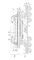
図1は、本発明の第1実施形態に係る半導体装置の概略構成を示す断面図である。
【0024】
図1において、半導体パッケージPK1にはキャリア基板1が設けられ、キャリア基板1の両面にはランド2a、2bがそれぞれ形成されている。そして、キャリア基板1上には半導体チップ3がフリップチップ実装され、半導体チップ3には、フリップチップ実装するための突出電極4が設けられている。そして、半導体チップ3に設けられた突出電極4は、異方性導電シート5を介してランド2b上にACF(Anisotropic Conductive Film)接合されている。
【0025】
一方、半導体パッケージPK2にはキャリア基板11が設けられ、キャリア基板11の裏面にはランド12が形成され、ランド12上には突出電極13が設けられている。また、キャリア基板11上には半導体チップが実装され、半導体チップが実装されたキャリア基板11は、封止樹脂14で封止されている。なお、キャリア基板11上には、ワイヤボンド接続された半導体チップを実装するようにしてもよいし、半導体チップをフリップチップ実装するようにしてもよく、半導体チップの積層構造を実装するようにしてもよい。
【0026】
そして、キャリア基板1上に設けられたランド2bに突出電極13を接合させることにより、キャリア基板11が半導体チップ3上に配置されるようにして、半導体パッケージPK2が半導体パッケージPK1上に実装されている。
また、半導体チップ3上には、半導体チップ3の少なくとも一部が露出するように樹脂15が配置され、半導体パッケージPK2は樹脂15を介して半導体チップ3に固着されている。ここで、樹脂15としては、樹脂ペーストまたは樹脂シートのいずれを用いるようにしてもよい。
【0027】
これにより、半導体チップ3上に配置された樹脂15を介して半導体パッケージPK1と半導体パッケージPK2とを固定することが可能となり、半導体パッケージPK1、PK2間に樹脂15を設けた場合においても、半導体パッケージPK1、PK2間に隙間を残すことが可能となる。このため、半導体パッケージPK1、PK2間の樹脂15に含まれる水分を抜け出し易くすることが可能となり、2次実装時に突出電極6のリフロー処理が行われる場合においても、半導体パッケージPK1、PK2間の樹脂15が膨張することを抑制することが可能となる。この結果、半導体パッケージPK1、PK2間の剥離を抑止することを可能としつつ、半導体パッケージPK1と半導体パッケージPK2とを樹脂15で固着させることが可能となり、半導体パッケージPK1、PK2間の位置ずれを防止することが可能となる。
【0028】
なお、樹脂15は、半導体パッケージPK2と半導体チップ3の対向面にのみ設けるようにしてもよい。これにより、半導体パッケージPK1に樹脂15を接触させることなく、半導体チップ3上に配置された樹脂15を介して半導体パッケージPK1と半導体パッケージPK2とを効率よく固着させることが可能となり、半導体パッケージPK1、PK2間の剥離を抑止することが可能としつつ、積層された半導体パッケージPK1、PK2の2次実装時の位置ずれを防止することが可能となる。
【0029】
また、樹脂15は、半導体チップ15の中央部に設けるようにしてもよい。これにより、突出電極13を介して半導体パッケージPK1と半導体パッケージPK2とを電気的に接続した場合においても、突出電極13から離れた位置に樹脂15を配置することが可能となる。このため、樹脂15の伸び縮みの影響が突出電極13に及ぶことを抑制することが可能となり、温度サイクルなどでの耐久性を向上させることが可能となる。
【0030】
また、半導体チップ3と半導体パッケージPK2との間に設けられた樹脂15は、半導体チップ3とキャリア基板1との間に設けられた異方性導電シート5よりも弾性率が低いことが好ましい。これにより、半導体チップ3に加わる衝撃を樹脂15に効率よく吸収させることが可能となる。このため、半導体チップ3の耐衝撃性を向上させることが可能となり、半導体チップ3の信頼性を確保しつつ、半導体パッケージPK1、PK2を積層することが可能となる。
【0031】
また、樹脂15には、シリカやアルミナなどのフィラーが混入されるようにしてもよい。これにより、樹脂15の粘度を容易に制御することが可能となり、樹脂15の液垂れを防止することを可能として、樹脂15の存在範囲を容易に制御することが可能となる。
また、半導体チップ3上の樹脂15は、1ヶ所にのみ配置されていてもよいが、半導体チップ3上に分散して配置するようにしてもよい。ここで、半導体チップ3上に樹脂15を分散して配置することにより、樹脂15に含まれる水分を逃がすための経路を半導体チップ3上に確保することが可能となり、半導体チップ3と半導体パッケージPK2との間の間隔が狭い場合においても、樹脂15に含まれる水分を減らすことが可能となる。
【0032】
また、キャリア基板1、11としては、例えば、両面基板、多層配線基板、ビルドアップ基板、テープ基板またはフィルム基板などを用いることができ、キャリア基板1、11の材質としては、例えば、ポリイミド樹脂、ガラスエポキシ樹脂、BTレジン、アラミドとエポキシのコンポジットまたはセラミックなどを用いることができる。また、突出電極4、6、13としては、例えば、Auバンプ、半田材などで被覆されたCuバンプやNiバンプ、あるいはハンダボールなどを用いることができる。
【0033】
さらに、突出電極13を介して半導体パッケージPK1、PK2を互いに接合させる場合、半田接合や合金接合などの金属接合を用いるようにしてもよく、ACF接合、NCF(Nonconductive Film)接合、ACP(Anisotropic Conductive Paste)接合、NCP(Nonconductive Paste)接合などの圧接接合を用いるようにしてもよい。また、上述した実施形態では、突出電極4を介して半導体チップ3をキャリア基板1にフリップチップ実装する場合、ACF接合を用いる方法について説明したが、NCF接合、ACP接合、NCP接合などの圧接接合を用いるようにしてもよく、半田接合や合金接合などの金属接合を用いるようにしてもよい。
【0034】
図2は、図1の半導体装置の製造方法の一例を示す断面図である。
図2(a)において、半導体パッケージPK1上に半導体パッケージPK2を積層する場合、半導体パッケージPK2のランド12上に、突出電極13としてハンダボールを形成するとともに、キャリア基板1のランド2b上にフラックス7を供給する。また、ディスペンサなどを用いることにより、半導体チップ3上に樹脂15を供給する。
【0035】
次に、図2(b)に示すように、半導体パッケージPK1上に半導体パッケージPK2をマウントする。そして、突出電極13のリフロー処理を行うことにより、突出電極13を溶融させ、突出電極13をランド2b上に接合させる。
ここで、突出電極13をランド2b上に接合させる場合、Aステージ状態(昇温により樹脂が軟化する状態)またはBステージ状態(昇温により、樹脂粘度が高くなる状態)に樹脂15を維持することが好ましい。これにより、突出電極13の溶融時の表面張力により、突出電極13をランド2b上に自己整合的に配置することが可能となり、半導体パッケージPK1上に半導体パッケージPK2を精度よく配置することが可能となる。そして、突出電極13がランド2b上に接合されると、突出電極13のリフロー時の温度よりも低い温度で樹脂15をキュアし、樹脂15をCステージ状態(硬化状態)に移行させる。
【0036】
ここで、半導体チップ3の少なくとも一部が露出するように半導体チップ3上に樹脂15を設けることにより、樹脂15に含まれる水分を逃がすための隙間を確保しつつ、半導体チップ3を介して半導体パッケージPK1、PK2を互いに固着させることが可能となるとともに、樹脂15に含まれる水分の残留量を減らすことが可能となる。
【0037】
次に、図2(c)に示すように、キャリア基板1の裏面に設けられたランド2a上に、キャリア基板1をマザー基板8上に実装するための突出電極6を形成する。
次に、図2(d)に示すように、突出電極6が形成されたキャリア基板1をマザー基板8上にマウントする。そして、突出電極6のリフロー処理を行うことにより、突出電極6をマザー基板8のランド9上に接合させる。
【0038】
ここで、半導体チップ3の少なくとも一部が露出するように半導体チップ3上に樹脂15を設けることにより、半導体パッケージPK1、PK2間の樹脂15に含まれる水分がほとんど除去された状態で、突出電極6のリフロー処理を行うことができる。このため、突出電極6のリフロー時に樹脂15が膨張することを抑制することが可能となり、半導体パッケージPK1、PK2が互いに剥離することを防止することが可能となる。また、突出電極6のリフロー時に突出電極13の再リフローが行われる場合においても、半導体パッケージPK1、PK2が樹脂15で互いに固定されたままの状態を維持することが可能となり、半導体パッケージPK1、PK2間の位置ずれを防止することが可能となる。
【0039】
なお、上述した実施形態では、半導体パッケージPK2を半導体パッケージPK1上に実装するために、キャリア基板1のランド2b上に突出電極13を設けるとともに、キャリア基板11のランド12上にラックス7を供給する方法について説明したが、キャリア基板1のランド2b上にフラックス7を供給するとともに、キャリア基板11のランド12上に突出電極13を設けるようにしてもよい。フラックス7の代わりにはんだペーストを用いても良い。また、上述した実施形態では、ディスペンサなどを用いることにより、半導体チップ3上にペースト状の樹脂15を供給する方法について説明したが、半導体チップ3上にシート状の樹脂15を供給するようにしてもよい。
【0040】
図3は、本発明の第2実施形態に係る半導体装置の概略構成を示す断面図である。
図3において、半導体パッケージPK11にはキャリア基板21が設けられ、キャリア基板21の両面にはランド22a、22cがそれぞれ形成されるとともに、キャリア基板21内には内部配線22bが形成されている。そして、キャリア基板21上には半導体チップ23がフリップチップ実装され、半導体チップ23には、フリップチップ実装するための突出電極24が設けられている。そして、半導体チップ23に設けられた突出電極24は、異方性導電シート25を介してランド22c上にACF接合されている。また、キャリア基板21の裏面に設けられたランド22a上には、キャリア基板21をマザー基板上に実装するための突出電極26が設けられている。
【0041】
一方、半導体パッケージPK12にはキャリア基板31が設けられ、キャリア基板31の両面にはランド32a、32cがそれぞれ形成されるとともに、キャリア基板31内には内部配線32bが形成されている。そして、キャリア基板31上には、接着層34aを介し半導体チップ33aがフェースアップ実装され、半導体チップ33aは、導電性ワイヤ35aを介してランド32cにワイヤボンド接続されている。さらに、半導体チップ33a上には、導電性ワイヤ35aを避けるようにして、半導体チップ33bがフェースアップ実装され、半導体チップ33bは、接着層34bを介して半導体チップ33a上に固定されるとともに、導電性ワイヤ35bを介してランド32cにワイヤボンド接続されている。
【0042】
また、キャリア基板31の裏面に設けられたランド32a上には、キャリア基板31が半導体チップ23上に保持されるようにして、キャリア基板31をキャリア基板21上に実装するための突出電極36が設けられている。ここで、突出電極36は、半導体チップ23の搭載領域を避けるようにして配置され、例えば、キャリア基板31の裏面の周囲に突出電極36を配置することができる。そして、キャリア基板21上に設けられたランド22cに突出電極36を接合させることにより、キャリア基板31がキャリア基板21上に実装されている。
【0043】
また、半導体チップ33a、33bの実装面側のキャリア基板31上には封止樹脂37が設けられ、この封止樹脂37により半導体チップ33a、33bが封止されている。なお、封止樹脂37で半導体チップ33a、33bを封止する場合、例えば、エポキシ樹脂などの熱硬化性樹脂を用いたモールド成形などにより行うことができる。
【0044】
また、半導体チップ23上には、半導体チップ23の少なくとも一部が露出するように樹脂38が配置され、半導体パッケージPK12は樹脂38を介して半導体チップ23に固着されている。
これにより、異種パッケージを積層した場合においても、突出電極36を介して接続されたキャリア基板21、31間に隙間を残したままの状態で、キャリア基板21、31間に樹脂38を設けることが可能となる。このため、サイズまたは種類の異なる半導体チップ23、33a、33bを実装する際の省スペース化を図ることが可能となるとともに、積層された半導体パッケージPK11、P12の2次実装時の位置ずれを防止しつつ、半導体パッケージPK11、P12間の剥離を抑止することが可能となる。
【0045】
図4は、本発明の第3実施形態に係る半導体装置の概略構成を示す断面図である。
図4において、半導体パッケージPK21にはキャリア基板41が設けられ、キャリア基板41の両面にはランド42a、42cがそれぞれ形成されるとともに、キャリア基板41内には内部配線42bが形成されている。そして、キャリア基板41上には、半導体チップ43がフリップチップ実装され、半導体チップ43には、フリップチップ実装するための突出電極44が設けられている。そして、半導体チップ43に設けられた突出電極44は、異方性導電シート45を介してランド42c上にACF接合されている。また、キャリア基板41の裏面に設けられたランド42a上には、キャリア基板41をマザー基板上に実装するための突出電極46が設けられている。
【0046】
一方、半導体パッケージPK22には半導体チップ51が設けられ、半導体チップ51には、電極パッド52が設けられるとともに、電極パッド52が露出するようにして、絶縁膜53が設けられている。そして、半導体チップ51上には、電極パッド52が露出するようにして応力緩和層54が形成され、電極パッド52上には、応力緩和層54上に延伸された再配置配線55が形成されている。そして、再配置配線55上にはソルダレジスト膜56が形成され、ソルダレジスト膜56には、応力緩和層54上において再配置配線55を露出させる開口部57が形成されている。そして、開口部57を介して露出された再配置配線55上には、半導体パッケージPK32が半導体チップ53上に保持されるように、半導体チップ51をキャリア基板41上にフェースダウン実装するための突出電極58が設けられている。
【0047】
ここで、突出電極58は、半導体チップ43の搭載領域を避けるようにして配置され、例えば、半導体チップ51の周囲に突出電極58を配置することができる。そして、キャリア基板41上に設けられたランド42c上に突出電極58が接合され、半導体パッケージPK22がキャリア基板41上に実装されている。
また、半導体チップ43上には、半導体チップ43の少なくとも一部が露出するように樹脂59が配置され、半導体パッケージPK22は樹脂59を介して半導体チップ43に固着されている。
【0048】
これにより、半導体パッケージPK21上にW−CSP(ウェハレベル−チップサイズパッケージ)を積層した場合においても、突出電極58を介して接合されたキャリア基板41と半導体チップ51との間に隙間を残したままの状態で、キャリア基板41と半導体チップ51との間に樹脂59を設けることが可能となる。このため、半導体チップ43、51の種類またはサイズが異なる場合においても、半導体チップ43、51間にキャリア基板を介在させることなく、半導体チップ43上に半導体チップ51を3次元実装することが可能となるとともに、積層された半導体パッケージPK21、P22の2次実装時の位置ずれを防止しつつ、半導体パッケージPK21、P22間の剥離を抑止することが可能となる。この結果、3次元実装された半導体チップ43、51の信頼性の劣化を抑制しつつ、半導体チップ43、51積層時の高さの増大を抑制することが可能となり、半導体チップ43、51実装時の省スペース化を図ることが可能となる。
【0049】
図5は、本発明の第4実施形態に係る半導体装置の構成を示す断面図である。
図5において、半導体パッケージPK31にはキャリア基板61が設けられ、キャリア基板61の両面にはランド62a、62bがそれぞれ形成されている。そして、キャリア基板61上には半導体チップ63がフリップチップ実装され、半導体チップ63には、フリップチップ実装するための突出電極64が設けられている。そして、半導体チップ63に設けられた突出電極64は、異方性導電シート65を介してランド62b上にACF接合されている。
【0050】
一方、半導体パッケージPK32、PK33にはキャリア基板71、81がそれぞれ設けられ、キャリア基板71、81の裏面にはランド72、82がそれぞれ形成され、ランド72、82上にはハンダボールなどの突出電極73、83がそれぞれ設けられている。また、キャリア基板71、81上には半導体チップがそれぞれ実装され、半導体チップが実装されたキャリア基板71、81は、封止樹脂74、84でそれぞれ封止されている。
【0051】
そして、キャリア基板61上に設けられたランド62bに突出電極73、83をそれぞれ接合させることにより、キャリア基板71、81の端部がそれぞれ半導体チップ63上に配置されるようにして、複数の半導体パッケージPK32、PK33が半導体パッケージPK31上に実装されている。
また、半導体チップ63上には、半導体チップ63の少なくとも一部が露出するように樹脂67が配置され、半導体パッケージPK32、PK33の端部は樹脂67を介して半導体チップ63に固着されている。
【0052】
これにより、半導体チップ63上に配置された樹脂67を介して複数の半導体パッケージPK32、PK33を半導体パッケージPK31に一括して固定することが可能となり、半導体パッケージPK32、PK33と半導体パッケージPK31との間に樹脂67を設けた場合においても、製造工程の煩雑化を抑制しつつ、半導体パッケージPK32、PK33と半導体パッケージPK31との間に隙間を残すことが可能となる。このため、実装面積をより一層縮小することを可能としつつ、半導体パッケージPK32、PK33と半導体パッケージPK31との間の剥離を抑止することが可能となるとともに、半導体パッケージPK31、PK32、PK33の2次実装時の位置ずれを防止することが可能となる。
【0053】
なお、半導体チップ63と半導体パッケージPK32、PK33との間に樹脂67をそれぞれ設ける場合、半導体チップ63上に樹脂67を供給してから、半導体チップ63上に半導体パッケージPK32、PK33をそれぞれ配置するようにしてもよい。また、半導体チップ63上に半導体パッケージPK32、PK33をそれぞれ配置した後に、半導体パッケージPK32、PK33間の隙間を介して、半導体チップ63上に樹脂67を供給するようにしてもよい。
【0054】
図6は、本発明の第5実施形態に係る半導体装置の構成を示す断面図である。図6において、半導体パッケージPK41にはキャリア基板91が設けられ、キャリア基板91の両面にはランド92a、92cがそれぞれ形成されるとともに、キャリア基板91内には内部配線92bが形成されている。そして、キャリア基板91上には半導体チップ93がフリップチップ実装され、半導体チップ93には、フリップチップ実装するための突出電極94が設けられている。そして、半導体チップ93に設けられた突出電極94は、異方性導電シート95を介してランド92c上にACF接合されている。また、キャリア基板91の裏面に設けられたランド92a上には、キャリア基板91をマザー基板上に実装するための突出電極96が設けられている。
【0055】
一方、半導体パッケージPK42、PK43にはキャリア基板101、201がそれぞれ設けられている。そして、キャリア基板101、201の裏面にはランド102a、202aがそれぞれ形成されるとともに、キャリア基板101、201の表面にはランド102c、202cがそれぞれ形成され、キャリア基板101、201内には内部配線102b、202bがそれぞれ形成されている。
【0056】
そして、キャリア基板101、201上には、接着層104a、204aをそれぞれ介し半導体チップ103a、203aがそれぞれフェースアップ実装され、半導体チップ103a、203aは、導電性ワイヤ105a、205aをそれぞれ介してランド102c、202cにそれぞれワイヤボンド接続されている。さらに、半導体チップ103a、203a上には、導電性ワイヤ105a、205aを避けるようにして、半導体チップ103b、203bがそれぞれフェースアップ実装され、半導体チップ103b、203bは、接着層104b、204bをそれぞれ介して半導体チップ103a、203a上にそれぞれ固定されるとともに、導電性ワイヤ105b、205bをそれぞれ介してランド102c、202cにそれぞれワイヤボンド接続されている。さらに、半導体チップ103b、203b上には、導電性ワイヤ105b、205bを避けるようにして、半導体チップ103c、203cがそれぞれフェースアップ実装され、半導体チップ103c、203cは、接着層104c、204cをそれぞれ介して半導体チップ103b、203b上にそれぞれ固定されるとともに、導電性ワイヤ105c、205cをそれぞれ介してランド102c、202cにそれぞれワイヤボンド接続されている。
【0057】
また、キャリア基板101、201の裏面にそれぞれ設けられたランド102a、202a上には、キャリア基板101、201が半導体チップ93上にそれぞれ保持されるようにして、キャリア基板101、201をキャリア基板91上にそれぞれ実装するための突出電極106、206がそれぞれ設けられている。ここで、突出電極106、206は、キャリア基板101、201の少なくとも四隅に存在することが好ましく、例えば、突出電極106、206をコ字状に配列することができる。
【0058】
そして、キャリア基板91上に設けられたランド92cに突出電極106、206をそれぞれ接合させることにより、キャリア基板101、201の端部がそれぞれ半導体チップ93上に配置されるようにして、キャリア基板101、201をキャリア基板91上にそれぞれ実装することができる。
また、半導体チップ103a〜103c、203a〜203cの実装面側のキャリア基板101、201には封止樹脂107、207がそれぞれ設けられ、この封止樹脂107、207により半導体チップ103a〜103c、203a〜203cがそれぞれ封止されている。
【0059】
また、半導体チップ93上には、半導体チップ93の少なくとも一部が露出するように樹脂97が配置され、半導体パッケージPK42、PK43の端部は樹脂97を介して半導体チップ93に固着されている。
これにより、同一の半導体チップ93上に複数の半導体パッケージPK42、PK43を配置することが可能となり、実装面積の縮小を可能としつつ、異種の半導体チップ93、103a〜103c、203a〜203cの3次元実装を図ることが可能となるととともに、半導体パッケージPK42、PK43と半導体パッケージPK41との間の剥離を抑止しつつ、半導体パッケージPK41、PK42、PK43の2次実装時の位置ずれを防止することが可能となる。
【0060】
なお、上述した半導体装置は、例えば、液晶表示装置、携帯電話、携帯情報端末、ビデオカメラ、デジタルカメラ、MD(Mini Disc)プレーヤなどの電子機器に適用することができ、電子機器の小型・軽量化を可能としつつ、電子機器の信頼性を向上させることができる。
また、上述した実施形態では、半導体パッケージを積層する方法を例にとって説明したが、本発明は、必ずしも半導体パッケージを積層する方法に限定されることなく、例えば、弾性表面波(SAW)素子などのセラミック素子、光変調器や光スイッチなどの光学素子、磁気センサやバイオセンサなどの各種センサ類などを積層する方法に用いるようにしてもよい。
【図面の簡単な説明】
【図1】第1実施形態に係る半導体装置の概略構成を示す断面図。
【図2】図1の半導体装置の製造方法の一例を示す断面図。
【図3】第2実施形態に係る半導体装置の概略構成を示す断面図。
【図4】第3実施形態に係る半導体装置の概略構成を示す断面図。
【図5】第4実施形態に係る半導体装置の概略構成を示す断面図。
【図6】第5実施形態に係る半導体装置の概略構成を示す断面図。
【符号の説明】
PK1、PK2、PK11、PK12、PK21、PK22、PK31、PK32、PK41、PK42 半導体パッケージ、1、11、21、31、41、61、71、81、91、101、201 キャリア基板、2a、2b、9、12、22a、22c、32a、32c、42a、42c、62a、62b、72、82、92a、92c、102a、102c、202a、202c ランド、3、23、33a、33b、43、51、63、93、103a、103b、103c、203a、203b、203c 半導体チップ、4、13、24、26、36、44、46、58、64、66、73、83、94、96、106、206 突出電極、5、25、45、65、95 異方性導電シート、7 フラックス、14、37、74、84、107、207 封止樹脂、15、38、59、67、97 樹脂、22b、32b、42b、92b102b、202b 内部配線、34a、34b、104a、104b、104c、204a、204b、204c 接着層、35a、35b、105a、105b、105c、205a、205b、205c 導電性ワイヤ、52 電極パッド、53 絶縁膜、54 応力緩和層、55 再配置配線、56 ソルダレジスト層、57 開口部
Claims (12)
- 第1半導体チップが搭載された第1半導体パッケージと、
前記第1半導体チップ上に配置されるようにして、前記第1半導体パッケージ上に支持された第2半導体パッケージと、
前記第1半導体チップの少なくとも一部が露出するように配置され、前記第1半導体チップと前記第2半導体パッケージとの間に設けられた樹脂とを備えることを特徴とする半導体装置。 - 第1半導体チップが搭載された第1半導体パッケージと、
前記第1半導体チップ上に端部が配置されるようにして、前記第1半導体パッケージ上に支持された第2半導体パッケージと、
前記第1半導体チップの少なくとも一部が露出するように配置され、前記第1半導体チップと前記第2半導体パッケージとの間に設けられた樹脂とを備えることを特徴とする半導体装置。 - 前記樹脂は、前記第2半導体パッケージと前記第1半導体チップの対向面にのみ設けられていることを特徴とする請求項1または2記載の半導体装置。
- 前記樹脂は前記第1半導体チップの中央部に設けられていることを特徴とする請求項1〜3のいずれか1項記載の半導体装置。
- 前記樹脂にはフィラーが混入されていることを特徴とする請求項1〜4のいずれか1項記載の半導体装置。
- 前記第1半導体パッケージは、
前記第1半導体チップがフリップチップ実装された第1キャリア基板と、
前記第1半導体チップと前記第1キャリア基板との間に設けられた樹脂層とを備え、
前記第2半導体パッケージは、
第2半導体チップと、
前記第2半導体チップが実装された第2キャリア基板と、
前記第1キャリア基板上に接合され、前記第1半導体チップ上に前記第2キャリア基板を保持する突出電極と、
前記第2半導体チップを封止する封止材とを備えることを特徴とする請求項1〜5いずれか1項記載の半導体装置。 - 前記突出電極はハンダボールであることを特徴とする請求項6記載の半導体装置。
- 前記第1半導体チップと前記第2半導体パッケージとの間に設けられた樹脂は、前記第1半導体チップと前記第1キャリア基板との間に設けられた樹脂層よりも弾性率が低いことを特徴とする請求項6または7記載の半導体装置。
- 前記第1半導体パッケージは、前記第1キャリア基板上に前記第1半導体チップがフリップチップ実装されたボールグリッドアレイ、前記第2半導体パッケージは、前記第2キャリア基板上に搭載された第2半導体チップがモールド封止されたボールグリッドアレイまたはチップサイズパッケージであることを特徴とする請求項6〜8のいずれか1項記載の半導体装置。
- 電子部品が搭載された第1パッケージと、
前記電子部品上に配置されるようにして、前記第1パッケージ上に支持された第2パッケージと、
前記電子部品の少なくとも一部が露出するように配置され、前記電子部品と前記第2パッケージとの間に設けられた樹脂とを備えることを特徴とする電子デバイス。 - 第1半導体チップが搭載された第1半導体パッケージと、前記第1半導体チップ上に配置されるようにして、前記第1半導体パッケージ上に支持された第2半導体パッケージと、
前記第1半導体チップの少なくとも一部が露出するように配置され、前記第1半導体チップと前記第2半導体パッケージとの間に設けられた樹脂と、
前記第2半導体パッケージが支持される前記第1半導体パッケージを搭載するマザー基板と、
前記マザー基板を介して前記第1半導体チップに接続された電子部品とを備えることを特徴とする電子機器。 - 第1半導体パッケージに搭載された第1半導体チップ上に樹脂を供給する工程と、
前記第1半導体チップの少なくとも一部が前記樹脂から露出するようにして、第2半導体チップが搭載された第2半導体パッケージを前記第1半導体パッケージ上に実装する工程とを備えることを特徴とする半導体装置の製造方法。
Priority Applications (3)
| Application Number | Priority Date | Filing Date | Title |
|---|---|---|---|
| JP2003127057A JP3786103B2 (ja) | 2003-05-02 | 2003-05-02 | 半導体装置、電子デバイス、電子機器および半導体装置の製造方法 |
| CNB2004100386412A CN100369249C (zh) | 2003-05-02 | 2004-04-27 | 半导体装置及其制造方法、电子设备、电子仪器 |
| US10/833,508 US20050001301A1 (en) | 2003-05-02 | 2004-04-28 | Semiconductor device, electronic device, electronic equipment, and method of manufacturing semiconductor device |
Applications Claiming Priority (1)
| Application Number | Priority Date | Filing Date | Title |
|---|---|---|---|
| JP2003127057A JP3786103B2 (ja) | 2003-05-02 | 2003-05-02 | 半導体装置、電子デバイス、電子機器および半導体装置の製造方法 |
Publications (3)
| Publication Number | Publication Date |
|---|---|
| JP2004335603A true JP2004335603A (ja) | 2004-11-25 |
| JP2004335603A5 JP2004335603A5 (ja) | 2005-11-04 |
| JP3786103B2 JP3786103B2 (ja) | 2006-06-14 |
Family
ID=33503749
Family Applications (1)
| Application Number | Title | Priority Date | Filing Date |
|---|---|---|---|
| JP2003127057A Expired - Lifetime JP3786103B2 (ja) | 2003-05-02 | 2003-05-02 | 半導体装置、電子デバイス、電子機器および半導体装置の製造方法 |
Country Status (3)
| Country | Link |
|---|---|
| US (1) | US20050001301A1 (ja) |
| JP (1) | JP3786103B2 (ja) |
| CN (1) | CN100369249C (ja) |
Cited By (4)
| Publication number | Priority date | Publication date | Assignee | Title |
|---|---|---|---|---|
| JP2007096278A (ja) * | 2005-08-31 | 2007-04-12 | Canon Inc | 積層型半導体装置およびその製造方法 |
| JP2012225669A (ja) * | 2011-04-15 | 2012-11-15 | Nikon Corp | 位置情報検出センサ、位置情報検出センサの製造方法、エンコーダ、モータ装置及びロボット装置 |
| US8339797B2 (en) | 2009-03-12 | 2012-12-25 | Murata Manufacturing Co., Ltd. | Package substrate |
| US8436462B2 (en) | 2010-03-26 | 2013-05-07 | Samsung Electronics Co., Ltd. | Semiconductor housing package, semiconductor package structure including the semiconductor housing package, and processor-based system including the semiconductor package structure |
Families Citing this family (10)
| Publication number | Priority date | Publication date | Assignee | Title |
|---|---|---|---|---|
| US7829989B2 (en) * | 2005-09-07 | 2010-11-09 | Alpha & Omega Semiconductor, Ltd. | Vertical packaged IC device modules with interconnected 3D laminates directly contacts wafer backside |
| WO2008010563A1 (fr) * | 2006-07-21 | 2008-01-24 | Nikon Corporation | Système optique à puissance variable, dispositif d'imagerie, procédé d'agrandissement variable d'un système optique à puissance variable |
| US8963312B2 (en) * | 2010-05-11 | 2015-02-24 | Xintec, Inc. | Stacked chip package and method for forming the same |
| US8680663B2 (en) * | 2012-01-03 | 2014-03-25 | Taiwan Semiconductor Manufacturing Company, Ltd. | Methods and apparatus for package on package devices with reduced strain |
| JP6252241B2 (ja) * | 2014-02-27 | 2017-12-27 | セイコーエプソン株式会社 | 力検出装置、およびロボット |
| CN104637998B (zh) * | 2015-02-06 | 2017-06-30 | 清华大学 | 一种提高晶闸管抗干扰能力的方法 |
| KR102502872B1 (ko) * | 2018-03-23 | 2023-02-23 | 가부시키가이샤 무라타 세이사쿠쇼 | 고주파 모듈 및 통신 장치 |
| WO2019181590A1 (ja) * | 2018-03-23 | 2019-09-26 | 株式会社村田製作所 | 高周波モジュールおよび通信装置 |
| TWI673834B (zh) * | 2018-09-26 | 2019-10-01 | 矽品精密工業股份有限公司 | 電子封裝件及其製法 |
| JP2021106341A (ja) * | 2019-12-26 | 2021-07-26 | 株式会社村田製作所 | 高周波モジュールおよび通信装置 |
Family Cites Families (8)
| Publication number | Priority date | Publication date | Assignee | Title |
|---|---|---|---|---|
| JPH09260436A (ja) * | 1996-03-27 | 1997-10-03 | Mitsubishi Electric Corp | 半導体装置 |
| JP3798597B2 (ja) * | 1999-11-30 | 2006-07-19 | 富士通株式会社 | 半導体装置 |
| JP2001210761A (ja) * | 2000-01-24 | 2001-08-03 | Shinko Electric Ind Co Ltd | 半導体装置及びその製造方法 |
| JP3798620B2 (ja) * | 2000-12-04 | 2006-07-19 | 富士通株式会社 | 半導体装置の製造方法 |
| DE10110203B4 (de) * | 2001-03-02 | 2006-12-14 | Infineon Technologies Ag | Elektronisches Bauteil mit gestapelten Halbleiterchips und Verfahren zu seiner Herstellung |
| JP2003007962A (ja) * | 2001-06-19 | 2003-01-10 | Toshiba Corp | 半導体積層モジュール |
| JP2003318361A (ja) * | 2002-04-19 | 2003-11-07 | Fujitsu Ltd | 半導体装置及びその製造方法 |
| JP2004349495A (ja) * | 2003-03-25 | 2004-12-09 | Seiko Epson Corp | 半導体装置、電子デバイス、電子機器および半導体装置の製造方法 |
-
2003
- 2003-05-02 JP JP2003127057A patent/JP3786103B2/ja not_active Expired - Lifetime
-
2004
- 2004-04-27 CN CNB2004100386412A patent/CN100369249C/zh not_active Expired - Fee Related
- 2004-04-28 US US10/833,508 patent/US20050001301A1/en not_active Abandoned
Cited By (5)
| Publication number | Priority date | Publication date | Assignee | Title |
|---|---|---|---|---|
| JP2007096278A (ja) * | 2005-08-31 | 2007-04-12 | Canon Inc | 積層型半導体装置およびその製造方法 |
| US7863101B2 (en) | 2005-08-31 | 2011-01-04 | Canon Kabushiki Kaisha | Stacking semiconductor device and production method thereof |
| US8339797B2 (en) | 2009-03-12 | 2012-12-25 | Murata Manufacturing Co., Ltd. | Package substrate |
| US8436462B2 (en) | 2010-03-26 | 2013-05-07 | Samsung Electronics Co., Ltd. | Semiconductor housing package, semiconductor package structure including the semiconductor housing package, and processor-based system including the semiconductor package structure |
| JP2012225669A (ja) * | 2011-04-15 | 2012-11-15 | Nikon Corp | 位置情報検出センサ、位置情報検出センサの製造方法、エンコーダ、モータ装置及びロボット装置 |
Also Published As
| Publication number | Publication date |
|---|---|
| JP3786103B2 (ja) | 2006-06-14 |
| US20050001301A1 (en) | 2005-01-06 |
| CN100369249C (zh) | 2008-02-13 |
| CN1542963A (zh) | 2004-11-03 |
Similar Documents
| Publication | Publication Date | Title |
|---|---|---|
| US7256072B2 (en) | Semiconductor device, electronic device, electronic apparatus, and method of manufacturing semiconductor device | |
| US8786102B2 (en) | Semiconductor device and method of manufacturing the same | |
| JP3597754B2 (ja) | 半導体装置及びその製造方法 | |
| JP4110992B2 (ja) | 半導体装置、電子デバイス、電子機器、半導体装置の製造方法および電子デバイスの製造方法 | |
| US7087989B2 (en) | Semiconductor device, electronic device, electronic apparatus, and method of manufacturing semiconductor device | |
| US8188585B2 (en) | Electronic device and method for producing a device | |
| US20040222510A1 (en) | Semiconductor device, semiconductor pack age, electronic device, electronic apparatus, and manufacturing methods of semiconductor device and electronic device | |
| US20040222508A1 (en) | Semiconductor device, electronic device, electronic apparatus, method of manufacturing semiconductor device, and method of manufacturing electronic device | |
| TWI236133B (en) | Semiconductor device and manufacturing method of same | |
| JP2004031607A (ja) | 半導体装置及びその製造方法 | |
| JP2003273317A (ja) | 半導体装置及びその製造方法 | |
| JP3786103B2 (ja) | 半導体装置、電子デバイス、電子機器および半導体装置の製造方法 | |
| JP4069771B2 (ja) | 半導体装置、電子機器および半導体装置の製造方法 | |
| KR20070076084A (ko) | 스택 패키지와 그 제조 방법 | |
| US8434664B2 (en) | Micro-ball loading device and loading method | |
| US7226808B2 (en) | Method of manufacturing semiconductor device and method of manufacturing electronics device | |
| US20050110166A1 (en) | Semiconductor device, electronic device, electronic apparatus, method of manufacturing semiconductor device, and method of manufacturing electronic device | |
| JP2011243724A (ja) | 半導体装置およびその製造方法 | |
| JP2004281919A (ja) | 半導体装置、電子デバイス、電子機器、半導体装置の製造方法および電子デバイスの製造方法 | |
| KR100726892B1 (ko) | 3차원 칩 적층 패키지 모듈 및 이의 제조방법 | |
| JP2004335604A (ja) | 半導体装置の製造方法および電子デバイスの製造方法 | |
| US8878070B2 (en) | Wiring board and method of manufacturing a semiconductor device | |
| KR20030054066A (ko) | 적층 패키지 및 그 제조 방법 | |
| WO2008097964A1 (en) | Micro-ball loading device and loading method | |
| KR100446913B1 (ko) | 칩 캐리어를 사용하지 않는 반도체 장치 및 그 제조 방법 |
Legal Events
| Date | Code | Title | Description |
|---|---|---|---|
| A521 | Written amendment |
Free format text: JAPANESE INTERMEDIATE CODE: A523 Effective date: 20050804 |
|
| A621 | Written request for application examination |
Free format text: JAPANESE INTERMEDIATE CODE: A621 Effective date: 20050804 |
|
| A871 | Explanation of circumstances concerning accelerated examination |
Free format text: JAPANESE INTERMEDIATE CODE: A871 Effective date: 20050804 |
|
| A975 | Report on accelerated examination |
Free format text: JAPANESE INTERMEDIATE CODE: A971005 Effective date: 20050818 |
|
| A977 | Report on retrieval |
Free format text: JAPANESE INTERMEDIATE CODE: A971007 Effective date: 20051201 |
|
| A131 | Notification of reasons for refusal |
Free format text: JAPANESE INTERMEDIATE CODE: A131 Effective date: 20051213 |
|
| A521 | Written amendment |
Free format text: JAPANESE INTERMEDIATE CODE: A523 Effective date: 20060203 |
|
| TRDD | Decision of grant or rejection written | ||
| A01 | Written decision to grant a patent or to grant a registration (utility model) |
Free format text: JAPANESE INTERMEDIATE CODE: A01 Effective date: 20060228 |
|
| A61 | First payment of annual fees (during grant procedure) |
Free format text: JAPANESE INTERMEDIATE CODE: A61 Effective date: 20060313 |
|
| R150 | Certificate of patent or registration of utility model |
Free format text: JAPANESE INTERMEDIATE CODE: R150 |
|
| FPAY | Renewal fee payment (event date is renewal date of database) |
Free format text: PAYMENT UNTIL: 20090331 Year of fee payment: 3 |
|
| FPAY | Renewal fee payment (event date is renewal date of database) |
Free format text: PAYMENT UNTIL: 20100331 Year of fee payment: 4 |
|
| FPAY | Renewal fee payment (event date is renewal date of database) |
Free format text: PAYMENT UNTIL: 20100331 Year of fee payment: 4 |
|
| FPAY | Renewal fee payment (event date is renewal date of database) |
Free format text: PAYMENT UNTIL: 20110331 Year of fee payment: 5 |
|
| FPAY | Renewal fee payment (event date is renewal date of database) |
Free format text: PAYMENT UNTIL: 20120331 Year of fee payment: 6 |
|
| FPAY | Renewal fee payment (event date is renewal date of database) |
Free format text: PAYMENT UNTIL: 20120331 Year of fee payment: 6 |
|
| FPAY | Renewal fee payment (event date is renewal date of database) |
Free format text: PAYMENT UNTIL: 20130331 Year of fee payment: 7 |
|
| FPAY | Renewal fee payment (event date is renewal date of database) |
Free format text: PAYMENT UNTIL: 20140331 Year of fee payment: 8 |
|
| S531 | Written request for registration of change of domicile |
Free format text: JAPANESE INTERMEDIATE CODE: R313531 |
|
| R350 | Written notification of registration of transfer |
Free format text: JAPANESE INTERMEDIATE CODE: R350 |