EP4489532A1 - Wiring board - Google Patents
Wiring board Download PDFInfo
- Publication number
- EP4489532A1 EP4489532A1 EP23759966.7A EP23759966A EP4489532A1 EP 4489532 A1 EP4489532 A1 EP 4489532A1 EP 23759966 A EP23759966 A EP 23759966A EP 4489532 A1 EP4489532 A1 EP 4489532A1
- Authority
- EP
- European Patent Office
- Prior art keywords
- region
- insulation layer
- wiring board
- wiring
- conductor
- Prior art date
- Legal status (The legal status is an assumption and is not a legal conclusion. Google has not performed a legal analysis and makes no representation as to the accuracy of the status listed.)
- Withdrawn
Links
Images



Classifications
-
- H—ELECTRICITY
- H05—ELECTRIC TECHNIQUES NOT OTHERWISE PROVIDED FOR
- H05K—PRINTED CIRCUITS; CASINGS OR CONSTRUCTIONAL DETAILS OF ELECTRIC APPARATUS; MANUFACTURE OF ASSEMBLAGES OF ELECTRICAL COMPONENTS
- H05K1/00—Printed circuits
- H05K1/02—Details
- H05K1/0213—Electrical arrangements not otherwise provided for
- H05K1/0237—High frequency adaptations
- H05K1/0242—Structural details of individual signal conductors, e.g. related to the skin effect
-
- H—ELECTRICITY
- H05—ELECTRIC TECHNIQUES NOT OTHERWISE PROVIDED FOR
- H05K—PRINTED CIRCUITS; CASINGS OR CONSTRUCTIONAL DETAILS OF ELECTRIC APPARATUS; MANUFACTURE OF ASSEMBLAGES OF ELECTRICAL COMPONENTS
- H05K1/00—Printed circuits
- H05K1/18—Printed circuits structurally associated with non-printed electric components
- H05K1/181—Printed circuits structurally associated with non-printed electric components associated with surface mounted components
-
- H—ELECTRICITY
- H05—ELECTRIC TECHNIQUES NOT OTHERWISE PROVIDED FOR
- H05K—PRINTED CIRCUITS; CASINGS OR CONSTRUCTIONAL DETAILS OF ELECTRIC APPARATUS; MANUFACTURE OF ASSEMBLAGES OF ELECTRICAL COMPONENTS
- H05K3/00—Apparatus or processes for manufacturing printed circuits
- H05K3/10—Apparatus or processes for manufacturing printed circuits in which conductive material is applied to the insulating support in such a manner as to form the desired conductive pattern
-
- H—ELECTRICITY
- H05—ELECTRIC TECHNIQUES NOT OTHERWISE PROVIDED FOR
- H05K—PRINTED CIRCUITS; CASINGS OR CONSTRUCTIONAL DETAILS OF ELECTRIC APPARATUS; MANUFACTURE OF ASSEMBLAGES OF ELECTRICAL COMPONENTS
- H05K3/00—Apparatus or processes for manufacturing printed circuits
- H05K3/22—Secondary treatment of printed circuits
- H05K3/28—Applying non-metallic protective coatings
-
- H—ELECTRICITY
- H05—ELECTRIC TECHNIQUES NOT OTHERWISE PROVIDED FOR
- H05K—PRINTED CIRCUITS; CASINGS OR CONSTRUCTIONAL DETAILS OF ELECTRIC APPARATUS; MANUFACTURE OF ASSEMBLAGES OF ELECTRICAL COMPONENTS
- H05K3/00—Apparatus or processes for manufacturing printed circuits
- H05K3/30—Assembling printed circuits with electric components, e.g. with resistors
- H05K3/32—Assembling printed circuits with electric components, e.g. with resistors electrically connecting electric components or wires to printed circuits
- H05K3/34—Assembling printed circuits with electric components, e.g. with resistors electrically connecting electric components or wires to printed circuits by soldering
- H05K3/3452—Solder masks
-
- H—ELECTRICITY
- H05—ELECTRIC TECHNIQUES NOT OTHERWISE PROVIDED FOR
- H05K—PRINTED CIRCUITS; CASINGS OR CONSTRUCTIONAL DETAILS OF ELECTRIC APPARATUS; MANUFACTURE OF ASSEMBLAGES OF ELECTRICAL COMPONENTS
- H05K3/00—Apparatus or processes for manufacturing printed circuits
- H05K3/38—Improvement of the adhesion between the insulating substrate and the metal
-
- H—ELECTRICITY
- H05—ELECTRIC TECHNIQUES NOT OTHERWISE PROVIDED FOR
- H05K—PRINTED CIRCUITS; CASINGS OR CONSTRUCTIONAL DETAILS OF ELECTRIC APPARATUS; MANUFACTURE OF ASSEMBLAGES OF ELECTRICAL COMPONENTS
- H05K3/00—Apparatus or processes for manufacturing printed circuits
- H05K3/38—Improvement of the adhesion between the insulating substrate and the metal
- H05K3/381—Improvement of the adhesion between the insulating substrate and the metal by special treatment of the substrate
-
- H—ELECTRICITY
- H05—ELECTRIC TECHNIQUES NOT OTHERWISE PROVIDED FOR
- H05K—PRINTED CIRCUITS; CASINGS OR CONSTRUCTIONAL DETAILS OF ELECTRIC APPARATUS; MANUFACTURE OF ASSEMBLAGES OF ELECTRICAL COMPONENTS
- H05K2203/00—Indexing scheme relating to apparatus or processes for manufacturing printed circuits covered by H05K3/00
- H05K2203/13—Moulding and encapsulation; Deposition techniques; Protective layers
- H05K2203/1377—Protective layers
Definitions
- the present invention relates to a wiring board and a mounting structure using the wiring board.
- Patent Document 1 discloses that a surface of a resin base material (insulation layer) is roughened to improve adhesion between a wiring pattern and the insulation layer.
- Patent Document 1 JP 2007-95828 A
- a wiring board includes an insulation layer having a first surface and a second surface opposite to the first surface, and a first wiring conductor located on the first surface.
- the first surface of the insulation layer includes a first region having a first arithmetic mean roughness and a second region having a second arithmetic mean roughness.
- the second arithmetic mean roughness is larger than the first arithmetic mean roughness, and the first wiring conductor is located from the first region to the second region.
- a mounting structure includes the above-mentioned wiring board and an element located on a surface of the wiring board.
- Patent Document 1 allows improved adhesion between the wiring pattern and the insulation layer but has a problem that the electrical characteristics deteriorate when the surface of the insulation layer is roughened. Therefore, a wiring board which has excellent electrical characteristics and in which a wiring conductor is less likely to be peeled off is demanded.
- the wiring board according to the present disclosure has a configuration as described in SOLUTION TO PROBLEM, thereby reducing deterioration in electrical characteristics and making the wiring conductor less likely to be peeled off.
- FIG. 1 is an explanatory view for explaining a wiring board 1 according to one embodiment of the present disclosure.
- a wiring board 1 according to one embodiment includes an insulation layer 2, an electrical conductor layer 3, and a solder resist 4.
- the insulation layer 2 includes a core insulation layer 21 and a build-up insulation layer 22.
- the core insulation layer 21 is not particularly limited as long as it is made of a material having insulation properties. Examples of the material having the insulation properties include resins such as an epoxy resin, a bismaleimide-triazine resin, a polyimide resin, and a polyphenylene ether resin. Two or more types of these resins may be mixed and used.
- the thickness of the core insulation layer 21 is not particularly limited, and is, for example, 40 ⁇ m or more and 1800 ⁇ m or less.
- the core insulation layer 21 may contain a reinforcing material.
- the reinforcing material include insulation fabric materials such as glass fiber, glass non-woven fabric, aramid non-woven fabric, aramid fiber, and polyester fiber. Two or more types of reinforcing materials may be used in combination.
- An inorganic insulation filler such as silica, barium sulfate, talc, clay, glass, calcium carbonate, or titanium oxide may be dispersed in the core insulation layer 21.
- a through-hole conductor 21a is located in the core insulation layer 21 to electrically connect the upper and lower surfaces of the core insulation layer 21.
- the through-hole conductor 21a is located in the through-hole penetrating from the upper surface to the lower surface of the core insulation layer 21.
- the through-hole conductor 21a is formed by, for example, metallic plating such as copper-plating.
- the through-hole conductor 21a is connected to the electrical conductor layer 3 formed on both surfaces of the core insulation layer 21.
- the through-hole conductor 21a may be located only on the inner wall surface of a through-hole or may be filled in the through-hole.
- a build-up layer in which the electrical conductor layer 3 and the build-up insulation layer 22 are alternately layered is located on the upper surface and the lower surface of the core insulation layer 21.
- the electrical conductor layer 3 is not limited as long as it is made of a conductor such as metal.
- the electrical conductor layer 3 is made of a metal foil such as a copper foil, a metal plating such as a copper plating, or the like.
- the thickness of the electrical conductor layer 3 is not particularly limited, and is, for example, 10 ⁇ m or more and 30 ⁇ m or less.
- the build-up insulation layer 22 is not particularly limited as long as it is made of a material having insulation properties.
- the material having the insulation properties include resins such as an epoxy resin, a bismaleimide-triazine resin, a polyimide resin, and a polyphenylene ether resin. Two or more types of these resins may be mixed and used.
- Each build-up insulation layer 22 may be made of the same resin or a different resin.
- the build-up insulation layer 22 and the core insulation layer 21 may be made of the same resin or different resins.
- An inorganic insulation filler such as silica, barium sulfate, talc, clay, glass, calcium carbonate, or titanium oxide may be dispersed in the build-up insulation layer 22.
- the thickness of the build-up insulation layer 22 is not particularly limited and is, for example, 25 ⁇ m or more and 40 ⁇ m or less. Each build-up insulation layer 22 may have the same thickness or may have a different thickness.
- a via-hole conductor 22a for electrically connecting the layers is formed in the build-up insulation layer 22.
- the via-hole conductor 22a is located in the via hole penetrating through the upper and lower surfaces of the build-up insulation layer 22.
- the via-hole conductor 22a is formed by, for example, metallic plating such as copper-plating.
- the via-hole conductor 22a is connected to the electrical conductor layer 3 located on both surfaces of the build-up insulation layer 22.
- the via-hole conductor 22a may be filled in the via-hole, or may be located only on an inner wall surface of the via-hole.
- the solder resist 4 may be located on the surface of the build-up layer.
- the solder resist 4 is made of a resin, and examples of the resin include an acrylic-modified epoxy resin.
- the solder resist 4 is provided with an opening for electrically connecting the electrical conductor layer 3 and an electrode of an element via the solder 5.
- Examples of the element include a semiconductor integrated circuit element and an optoelectronic element.
- the build-up insulation layer 22 has a first surface 221 and a second surface 222 opposite to the first surface 221.
- FIG. 2 is an enlarged explanatory view for explaining one embodiment of a cross section of a region X illustrated in FIG. 1 .
- the first surface 221 includes a first region 2a having a first arithmetic mean roughness and a second region 2b having a second arithmetic mean roughness.
- the second arithmetic mean roughness of the second region 2b is larger than the first arithmetic mean roughness of the first region 2a.
- the first wiring conductor 31 is located from the first region 2a to the second region 2b. In this manner, since the first wiring conductor 31 is located in the regions having different arithmetic mean roughnesses, the deterioration of the electrical characteristics in the first region 2a having a small arithmetic mean roughness can be reduced and the adhesion of the first wiring conductor 31 in the second region 2b having a large arithmetic mean roughness can be improved. As a result, in the wiring board 1, deterioration of electrical characteristics is reduced, and the first wiring conductor 31 is less likely to be peeled off.
- the electrical conductor layer 3 generally includes a power supply conductor, a ground conductor, and a signal conductor.
- the first wiring conductor 31 is, for example, a signal conductor.
- the arithmetic mean roughness (third arithmetic mean roughness) of a side surface of the first wiring conductor 31 and the surface opposite to the surface in contact with the first surface 221 may be smaller than the first arithmetic mean roughness.
- the third arithmetic mean roughness is smaller than the first arithmetic mean roughness, the side surface and the surface of the first wiring conductor 31 are relatively flat, which is particularly advantageous in that the transmission characteristics are improved when a high-frequency signal is transmitted.
- the second arithmetic mean roughness may be at least 1.5 times the first arithmetic mean roughness.
- the second arithmetic mean roughness is at least 1.5 times the first arithmetic mean roughness, a relatively rough region and a smooth region are present, and the adhesion of the first wiring conductor 31 can be further improved while reducing the deterioration of the electrical characteristics.
- the first arithmetic mean roughness may be, for example, 50 nm or more and 200 nm or less
- the second arithmetic mean roughness may be, for example, 100 nm or more and 300 nm or less.
- At least one first region 2a and at least one second region 2b are provided for each first wiring conductor 31.
- the first region 2a and the second region 2b may be alternately located along the first wiring conductor 31 in consideration of the reduction of the deterioration of the electrical characteristics and the improvement of the adhesion of the first wiring conductor 31.
- the second region 2b may have a recessed portion 2c recessed toward the second surface 222.
- FIG. 3 is an enlarged explanatory view for explaining another embodiment of the cross section of the region X illustrated in FIG. 1 .
- the arithmetic mean roughness of the recessed portion 2c may be 100 nm or more and 300 nm or less, similarly to the second arithmetic mean roughness of the second region 2b.
- the size of the recessed portion 2c is not limited, and for example, the depth (D in FIG. 3 ) is 5 ⁇ m or less at the deepest portion, and the opening width (W in FIG. 3 ) is 10 ⁇ m or more and 200 ⁇ m or less at the maximum portion.
- the depth D and the opening width W of the recessed portion 2c are in such ranges, the surface of the first wiring conductor 31 (the surface opposite to the recessed portion 2c) can be kept flat. As a result, the adhesion of the first wiring conductor 31 can be further improved without affecting the electrical characteristics.
- the wiring board 1 may include a second wiring conductor 32.
- FIG. 4 is an enlarged explanatory view for explaining a cross section of a region Y illustrated in FIG. 1 .
- the second wiring conductor 32 is located on the second surface 222 of the build-up insulation layer 22, and is located overlapping the first region 2a of the build-up insulation layer 22 in a plane perspective.
- the second wiring conductor 32 is located between the build-up insulation layer 22 and the core insulation layer 21 in a state of being partially embedded in the build-up insulation layer 22, and the second wiring conductor 32 is located below the first region 2a in a cross-sectional view.
- the thickness of the build-up insulation layer 22 located on the upper surface of the second wiring conductor 32 is reduced. Therefore, since the second wiring conductor 32 faces the first region 2a having a small arithmetic mean roughness, the possibility of migration or a short circuit can be reduced, and the deterioration of the electrical characteristics can be reduced.
- the thickness of the second wiring conductor 32 is, for example, 20 ⁇ m or more and 30 ⁇ m or less.
- the distance between the adjacent second wiring conductors 32 is, for example, 30 ⁇ m or more and 50 ⁇ m or less.
- the first region 2a and the second region 2b of the insulation layer 2 are formed, for example, as follows.
- the insulation layer 2 for example, the core insulation layer 21
- the second wiring conductor 32 is formed on the surface of the core insulation layer 21 on which a surface (build-up insulation layer 22) is formed.
- the resin sheet 23 to be the build-up insulation layer 22 is layered on the surface of the core insulation layer 21 so as to cover the second wiring conductor 32.
- the resin sheet 23 to which a protective film 23a is attached is used.
- the protective film 23a has irregularities on the surface in contact with the resin sheet 23 while being attached to the surface of the resin sheet 23 on the side opposite to the core insulation layer 21.
- the resin sheet 23 is layered at a relatively high temperature (120°C or higher).
- the resin sheet 23 is pressurized from above the protective film 23a.
- the portion where the second wiring conductor 32 is present is pressurized more strongly than the other portion with the second wiring conductor 32 serving as a base.
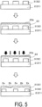
- the protective film 23a attached to the resin sheet 23 is peeled off, thereby forming the first region 2a and the second region 2b on the surface (first surface 221) of the build-up insulation layer 22.
- the portion strongly pressurized with the second wiring conductor 32 serving as a base has a small roughness and becomes the first region 2a. The roughness of the other portion is increased, and as illustrated in FIG. 5 , the second region 2b is formed.
- the first wiring conductor 31 is formed on the upper surface of the build-up insulation layer 22 from the first region 2a to the second region 2b by a semi-additive method.
- a metal oxide film such as an oxide film of copper is removed by acid cleaning.
- tin is precipitated so as to be as thick as 100 nm.
- excessively precipitated tin is removed, for example, by etching with nitric acid. The etching is performed in this manner to adjust the tin thickness to about 2 nm or more and 5 nm or less.
- the resin sheet 23 to be the build-up insulation layer 22 is layered on the surface of the core insulation layer 21 at a relatively low temperature (100°C or less), as illustrated in FIG. 6 , a recess is formed in the surface of the resin sheet 23 in a region between the adjacent second wiring conductors 32.
- a release film is interposed on the surface of the resin sheet from which the protective film 23a has been peeled off, and pressure is applied from above the release film.
- the resin sheet 23 to which the protective film 23a is attached is used.
- the protective film 23a has irregularities on the surface in contact with the resin sheet 23 while being attached to the surface of the resin sheet 23 on the side opposite to the core insulation layer 21.
- the recessed portion of the surface of the resin sheet 23 is not easily pressurized, and the roughness is likely to increase.
- the portion where the second wiring conductor 32 exists is strongly pressurized as described above, and the roughness becomes small.
- the first region 2a and the second region 2b having the recessed portion 2c are formed on the surface (first surface 221) of the build-up insulation layer 22. Due to the presence of the second wiring conductor 32, the recessed portion 2c is easily formed between the adjacent second wiring conductors 32.
- a mounting structure includes the wiring board 1 according to one embodiment and an element S located on a surface of the wiring board 1.
- the electrical conductor layer 3 in the opening of the solder resist 4 and the electrode of the element S are connected via the solder 5.
- examples of the element S include a semiconductor integrated circuit element and an optoelectronic element.
- the element S may be located on both surfaces of the wiring board 1, or the element S may be located on one surface of the wiring board 1 and a motherboard, for example, may be located on the other surface thereof.
- the wiring board according to the present disclosure is not limited to the wiring board 1 according to the above-described embodiment.
- the build-up insulation layer 22 located directly on the core insulation layer 21 includes the first region 2a and the second region 2b.
- the insulation layer included in the first region 2a and the second region 2b is not limited to the build-up insulation layer 22 located directly on the core insulation layer 21.
- the first region 2a and the second region 2b may be present on the first surface of the build-up insulation layer 22 other than the build-up insulation layer located directly on the core insulation layer, and the first region 2a and the second region 2b may be present on the first surface of the core insulation layer 21.
- the first region 2a and the second region 2b do not need to be present on the first surfaces of all the insulation layers, and the first region 2a and the second region 2b are present on the first surface of at least one insulation layer.
Landscapes
- Engineering & Computer Science (AREA)
- Microelectronics & Electronic Packaging (AREA)
- Manufacturing & Machinery (AREA)
- Production Of Multi-Layered Print Wiring Board (AREA)
- Laminated Bodies (AREA)
Applications Claiming Priority (2)
| Application Number | Priority Date | Filing Date | Title |
|---|---|---|---|
| JP2022029334 | 2022-02-28 | ||
| PCT/JP2023/006187 WO2023162965A1 (ja) | 2022-02-28 | 2023-02-21 | 配線基板 |
Publications (1)
| Publication Number | Publication Date |
|---|---|
| EP4489532A1 true EP4489532A1 (en) | 2025-01-08 |
Family
ID=87765907
Family Applications (1)
| Application Number | Title | Priority Date | Filing Date |
|---|---|---|---|
| EP23759966.7A Withdrawn EP4489532A1 (en) | 2022-02-28 | 2023-02-21 | Wiring board |
Country Status (7)
| Country | Link |
|---|---|
| US (1) | US20250168970A1 (https=) |
| EP (1) | EP4489532A1 (https=) |
| JP (1) | JP7778219B2 (https=) |
| KR (1) | KR20240141302A (https=) |
| CN (1) | CN118765538A (https=) |
| TW (1) | TWI866088B (https=) |
| WO (1) | WO2023162965A1 (https=) |
Family Cites Families (8)
| Publication number | Priority date | Publication date | Assignee | Title |
|---|---|---|---|---|
| JPH1051113A (ja) * | 1996-07-29 | 1998-02-20 | Ibiden Co Ltd | 多層プリント配線板の製造方法 |
| JP2007095828A (ja) | 2005-09-27 | 2007-04-12 | Dainippon Printing Co Ltd | パターン形成体 |
| JP5855905B2 (ja) * | 2010-12-16 | 2016-02-09 | 日本特殊陶業株式会社 | 多層配線基板及びその製造方法 |
| JP6380626B1 (ja) * | 2017-07-19 | 2018-08-29 | オムロン株式会社 | 樹脂構造体の製造方法および樹脂構造体 |
| JP6550196B2 (ja) * | 2017-07-24 | 2019-07-24 | 古河電気工業株式会社 | 表面処理銅箔、並びにこれを用いた銅張積層板およびプリント配線板 |
| WO2019117261A1 (ja) | 2017-12-15 | 2019-06-20 | 積水化学工業株式会社 | 積層フィルム及びプリント配線板用組み合わせ部材 |
| JP2019127571A (ja) | 2018-01-26 | 2019-08-01 | 日立化成株式会社 | 絶縁層用樹脂組成物、シート状積層材料、多層プリント配線板及び半導体装置 |
| JP2022030289A (ja) | 2020-08-06 | 2022-02-18 | イビデン株式会社 | 配線基板及び配線基板の製造方法 |
-
2023
- 2023-02-21 KR KR1020247028762A patent/KR20240141302A/ko not_active Withdrawn
- 2023-02-21 EP EP23759966.7A patent/EP4489532A1/en not_active Withdrawn
- 2023-02-21 WO PCT/JP2023/006187 patent/WO2023162965A1/ja not_active Ceased
- 2023-02-21 CN CN202380023743.8A patent/CN118765538A/zh not_active Withdrawn
- 2023-02-21 JP JP2024503165A patent/JP7778219B2/ja active Active
- 2023-02-21 US US18/841,569 patent/US20250168970A1/en active Pending
- 2023-02-23 TW TW112106761A patent/TWI866088B/zh active
Also Published As
| Publication number | Publication date |
|---|---|
| JP7778219B2 (ja) | 2025-12-01 |
| TW202344156A (zh) | 2023-11-01 |
| JPWO2023162965A1 (https=) | 2023-08-31 |
| WO2023162965A1 (ja) | 2023-08-31 |
| CN118765538A (zh) | 2024-10-11 |
| TWI866088B (zh) | 2024-12-11 |
| KR20240141302A (ko) | 2024-09-26 |
| US20250168970A1 (en) | 2025-05-22 |
Similar Documents
| Publication | Publication Date | Title |
|---|---|---|
| JP6885800B2 (ja) | 配線基板およびその製造方法 | |
| KR101277980B1 (ko) | 다층배선기판 | |
| JP2018504776A (ja) | プリント回路基板のための高速インターコネクト | |
| JPWO2013161527A1 (ja) | 多層配線基板及びその製造方法 | |
| CN108076587A (zh) | 具有附着增强形状的布线结构的部件承载件 | |
| KR101201940B1 (ko) | 케이블부를 가지는 다층 배선기판의 제조방법 | |
| KR102078009B1 (ko) | 인쇄회로기판 및 그 제조방법 | |
| EP4489532A1 (en) | Wiring board | |
| US9655242B2 (en) | Printed wiring board | |
| JP3674662B2 (ja) | 配線基板の製造方法 | |
| US20240422900A1 (en) | Wiring board and manufacturing method for the same | |
| EP4503872A1 (en) | Circuit board | |
| JP7583680B2 (ja) | 配線基板およびその製造方法 | |
| CN118338525A (zh) | 布线基板 | |
| US20170256470A1 (en) | Wiring substrate and method for manufacturing the same | |
| JP2022182717A (ja) | 配線基板及び配線基板の製造方法 | |
| KR100797669B1 (ko) | 인쇄회로기판 및 그 제조방법 | |
| US20240008191A1 (en) | Wiring substrate | |
| US20230397335A1 (en) | Wiring substrate | |
| US20240339393A1 (en) | Wiring substrate | |
| US20240237203A1 (en) | Wiring substrate | |
| TW202425721A (zh) | 配線基板及配線基板之製造方法 | |
| CN117412469A (zh) | 布线基板 | |
| WO2024135456A1 (ja) | 配線基板およびその製造方法 | |
| CN117098306A (zh) | 布线基板 |
Legal Events
| Date | Code | Title | Description |
|---|---|---|---|
| STAA | Information on the status of an ep patent application or granted ep patent |
Free format text: STATUS: THE INTERNATIONAL PUBLICATION HAS BEEN MADE |
|
| PUAI | Public reference made under article 153(3) epc to a published international application that has entered the european phase |
Free format text: ORIGINAL CODE: 0009012 |
|
| STAA | Information on the status of an ep patent application or granted ep patent |
Free format text: STATUS: REQUEST FOR EXAMINATION WAS MADE |
|
| 17P | Request for examination filed |
Effective date: 20240827 |
|
| AK | Designated contracting states |
Kind code of ref document: A1 Designated state(s): AL AT BE BG CH CY CZ DE DK EE ES FI FR GB GR HR HU IE IS IT LI LT LU LV MC ME MK MT NL NO PL PT RO RS SE SI SK SM TR |
|
| DAV | Request for validation of the european patent (deleted) | ||
| DAX | Request for extension of the european patent (deleted) | ||
| STAA | Information on the status of an ep patent application or granted ep patent |
Free format text: STATUS: THE APPLICATION HAS BEEN WITHDRAWN |
|
| 18W | Application withdrawn |
Effective date: 20251112 |