EP4268364B1 - Mit mehreren konfigurationen betreibbare leistungsverwaltungsvorrichtung - Google Patents
Mit mehreren konfigurationen betreibbare leistungsverwaltungsvorrichtung Download PDFInfo
- Publication number
- EP4268364B1 EP4268364B1 EP21806074.7A EP21806074A EP4268364B1 EP 4268364 B1 EP4268364 B1 EP 4268364B1 EP 21806074 A EP21806074 A EP 21806074A EP 4268364 B1 EP4268364 B1 EP 4268364B1
- Authority
- EP
- European Patent Office
- Prior art keywords
- voltage
- circuit
- reference voltage
- power management
- generate
- Prior art date
- Legal status (The legal status is an assumption and is not a legal conclusion. Google has not performed a legal analysis and makes no representation as to the accuracy of the status listed.)
- Active
Links
Images

Classifications
-
- H—ELECTRICITY
- H03—ELECTRONIC CIRCUITRY
- H03F—AMPLIFIERS
- H03F1/00—Details of amplifiers with only discharge tubes, only semiconductor devices or only unspecified devices as amplifying elements
- H03F1/02—Modifications of amplifiers to raise the efficiency, e.g. gliding Class A stages, use of an auxiliary oscillation
- H03F1/0205—Modifications of amplifiers to raise the efficiency, e.g. gliding Class A stages, use of an auxiliary oscillation in transistor amplifiers
- H03F1/0211—Modifications of amplifiers to raise the efficiency, e.g. gliding Class A stages, use of an auxiliary oscillation in transistor amplifiers with control of the supply voltage or current
- H03F1/0216—Continuous control
- H03F1/0222—Continuous control by using a signal derived from the input signal
-
- H—ELECTRICITY
- H02—GENERATION; CONVERSION OR DISTRIBUTION OF ELECTRIC POWER
- H02M—APPARATUS FOR CONVERSION BETWEEN AC AND AC, BETWEEN AC AND DC, OR BETWEEN DC AND DC, AND FOR USE WITH MAINS OR SIMILAR POWER SUPPLY SYSTEMS; CONVERSION OF DC OR AC INPUT POWER INTO SURGE OUTPUT POWER; CONTROL OR REGULATION THEREOF
- H02M1/00—Details of apparatus for conversion
- H02M1/0045—Converters combining the concepts of switch-mode regulation and linear regulation, e.g. linear pre-regulator to switching converter, linear and switching converter in parallel, same converter or same transistor operating either in linear or switching mode
-
- H—ELECTRICITY
- H02—GENERATION; CONVERSION OR DISTRIBUTION OF ELECTRIC POWER
- H02M—APPARATUS FOR CONVERSION BETWEEN AC AND AC, BETWEEN AC AND DC, OR BETWEEN DC AND DC, AND FOR USE WITH MAINS OR SIMILAR POWER SUPPLY SYSTEMS; CONVERSION OF DC OR AC INPUT POWER INTO SURGE OUTPUT POWER; CONTROL OR REGULATION THEREOF
- H02M3/00—Conversion of DC power input into DC power output
- H02M3/02—Conversion of DC power input into DC power output without intermediate conversion into AC
- H02M3/04—Conversion of DC power input into DC power output without intermediate conversion into AC by static converters
- H02M3/06—Conversion of DC power input into DC power output without intermediate conversion into AC by static converters using resistors or capacitors, e.g. potential divider
- H02M3/07—Conversion of DC power input into DC power output without intermediate conversion into AC by static converters using resistors or capacitors, e.g. potential divider using capacitors charged and discharged alternately by semiconductor devices with control electrode, e.g. charge pumps
-
- H—ELECTRICITY
- H03—ELECTRONIC CIRCUITRY
- H03F—AMPLIFIERS
- H03F1/00—Details of amplifiers with only discharge tubes, only semiconductor devices or only unspecified devices as amplifying elements
- H03F1/02—Modifications of amplifiers to raise the efficiency, e.g. gliding Class A stages, use of an auxiliary oscillation
- H03F1/0205—Modifications of amplifiers to raise the efficiency, e.g. gliding Class A stages, use of an auxiliary oscillation in transistor amplifiers
- H03F1/0211—Modifications of amplifiers to raise the efficiency, e.g. gliding Class A stages, use of an auxiliary oscillation in transistor amplifiers with control of the supply voltage or current
- H03F1/0216—Continuous control
- H03F1/0222—Continuous control by using a signal derived from the input signal
- H03F1/0227—Continuous control by using a signal derived from the input signal using supply converters
-
- H—ELECTRICITY
- H03—ELECTRONIC CIRCUITRY
- H03F—AMPLIFIERS
- H03F3/00—Amplifiers with only discharge tubes or only semiconductor devices as amplifying elements
- H03F3/189—High-frequency amplifiers, e.g. radio frequency amplifiers
- H03F3/19—High-frequency amplifiers, e.g. radio frequency amplifiers with semiconductor devices only
-
- H—ELECTRICITY
- H03—ELECTRONIC CIRCUITRY
- H03F—AMPLIFIERS
- H03F3/00—Amplifiers with only discharge tubes or only semiconductor devices as amplifying elements
- H03F3/20—Power amplifiers, e.g. Class B amplifiers, Class C amplifiers
- H03F3/21—Power amplifiers, e.g. Class B amplifiers, Class C amplifiers with semiconductor devices only
- H03F3/211—Power amplifiers, e.g. Class B amplifiers, Class C amplifiers with semiconductor devices only using a combination of several amplifiers
-
- H—ELECTRICITY
- H03—ELECTRONIC CIRCUITRY
- H03F—AMPLIFIERS
- H03F2200/00—Indexing scheme relating to amplifiers
- H03F2200/451—Indexing scheme relating to amplifiers the amplifier being a radio frequency amplifier
Definitions
- the technology of the disclosure relates generally to a power management apparatus.
- 5G-NR Fifth generation (5G) new radio (NR)
- 5G-NR has been widely regarded as the next generation of wireless communication technology beyond the current third generation (3G) and fourth generation (4G) technologies.
- a wireless communication device capable of supporting the 5G-NR wireless communication technology is expected to achieve higher data rates, improved coverage range, enhanced signaling efficiency, and reduced latency across a wide range of licensed radio frequency (RF) spectrum, which can include low-band spectrum (below 1 GHz), mid-band spectrum (1 GHz to 6 GHz), and high-band spectrum (above s24 GHz).
- RF radio frequency
- the wireless communication device is also required to support local area networking technologies, such as Wi-Fi, in unlicensed 2.4 GHz and 5 GHz spectrums. Further, it may be necessary for the wireless communication device to support both licensed and unlicensed spectrums concurrently to enable communications based on, for example, licensed-assisted access (LAA) scheme. As such, it is desirable to ensure the wireless communication device can operate with flexible multi-band radio frequency (RF) front-end configurations to help reduce complexity and footprint.
- LAA licensed-assisted access
- US 2018/152144 A1 discusses a supply modulator for providing a first power supply voltage and a second power supply voltage to a first power amplifier and a second power amplifier, respectively, and includes a first modulation circuit including a linear regulator and a switching regulator, the first modulation circuit being configured to generate a first modulation voltage in accordance with envelope tracking, and provide the first modulation voltage to the first power amplifier as the first power supply voltage; and a single inductor multiple output converter configured to generate a first output voltage and a second output voltage based on an input voltage having a fixed level, provide the first output voltage to the linear regulator of the first modulation circuit as a power supply voltage, and provide the second output voltage to the second power amplifier as the second power supply voltage.
- a supply modulator for providing a first power supply voltage and a second power supply voltage to a first power amplifier and a second power amplifier, respectively, and includes a first modulation circuit including a linear regulator and a switching regulator, the first modulation circuit being configured to generate a first modulation voltage in accordance
- Embodiments of the disclosure relate to a power management apparatus operatable with multiple configurations.
- the power management apparatus can be configured to concurrently generate multiple modulated voltages based on a configuration including a single power management integrated circuit (PMIC) or a configuration including a PMIC and a distributed PMIC.
- PMIC power management integrated circuit
- the power management apparatus employs a single switcher circuit, wherein multiple reference voltage circuits are configured to share a multi-level charge pump (MCP).
- MCP multi-level charge pump
- Embodiments of the disclosure relate to a power management apparatus operable with multiple configurations.
- the power management apparatus can be configured to concurrently generate multiple modulated voltages based on a configuration including a single power management integrated circuit (PMIC) or a configuration including a PMIC and a distributed PMIC.
- PMIC power management integrated circuit
- the power management apparatus employs a single switcher circuit, wherein multiple reference voltage circuits are configured to share a multi-level charge pump (MCP).
- MCP multi-level charge pump
- Figure 1 is a schematic diagram of an exemplary power management apparatus 10 configured according to an embodiment of the present disclosure to include a PMIC 12.
- the PMIC 12 is configured to include a first voltage circuit 14A and a second voltage circuit 14B.
- the first voltage circuit 14A is configured to generate a first modulated voltage V CCA based on a first target voltage V TGTA and a first reference voltage V REFA .
- the second voltage circuit 14B is configured to generate a second modulated voltage V CCB based on a second target voltage V TGTB and a second reference voltage V REFB .
- the first modulated voltage V CCA and the second modulated voltage V CCB can be envelope tracking (ET) voltages or average power tracking (APT) voltages.
- ET envelope tracking
- APT average power tracking
- the PMIC 12 also includes a switcher circuit 16, which is shared by the first voltage circuit 14A and the second voltage circuit 14B.
- the switcher circuit 16 includes a multi-level charge pump (MCP) 18.
- MCP multi-level charge pump
- the MCP 18 is configured to generate a low-frequency voltage V DC (e.g., a direct-current (DC) voltage) at a coupling node LX, as a function of a battery voltage V BAT .
- V DC direct-current
- the MCP 18 can be a buck-boost DC-DC converter that can operate in a buck mode to generate the low-frequency voltage V DC at 0 volt (V) or at V BAT or operate in a boost mode to generate the low-frequency voltage V DC at 2V BAT .
- the switcher circuit 16 also includes a first reference voltage circuit 20A and a second reference voltage circuit 20B.
- the first reference voltage circuit 20A and the second reference voltage circuit 20B are both coupled to the coupling node LX to share the MCP 18.
- the MCP 18 By sharing the MCP 18 between the first reference voltage circuit 20A and the second reference voltage circuit 20B, it is possible to reduce footprint of the power management apparatus 10 while improving isolation between the first modulated voltage V CCA and the second modulated voltage V CCB .
- the first reference voltage circuit 20A is coupled between the coupling node LX and the first voltage circuit 14A
- the second reference voltage circuit 20B is coupled between the coupling node LX and the second voltage circuit 14B.
- the first voltage circuit 14A and the second voltage circuit 14B are each configured to generate a respective one of the first reference voltage V REFA and the second reference voltage V REFB based on the low-frequency voltage V DC .
- the PMIC 12 further includes a control circuit 22, which can be a field-programmable gate array (FPGA) or an application-specific integrated circuit (ASIC), as an example.
- the control circuit 22 is configured to determine an appropriate duty cycle based on a selected one of the first target voltage V TGTA and the second target voltage V TGTB to thereby cause the MCP 18 to generate the low-frequency voltage V DC at a desirable level.
- Each of the first reference voltage circuit 20A and the second reference voltage circuit 20B may be an inductor-capacitor (LC) circuit.
- the first reference voltage circuit 20A includes a first inductor L A and a first capacitor C A and the second reference voltage circuit 20B includes a second inductor L B and a second capacitor C B .
- the first reference voltage circuit 20A and the second reference voltage circuit 20B can each resonate at a respective resonance frequency to generate a respective one of the first reference voltage V REFA and the second reference voltage V REFB as an average of the low-frequency voltage V DC .
- the battery voltage V BAT is 5 V and the MCP 18 is configured to toggle between 0 V, V BAT (5 V), and 2V BAT (10 V) based on a 30-30-40 duty cycle, then the average of the low-frequency voltage V DC will equal 5.5 V (0 V * 30% + 5 V * 30% + 10 V * 40%).
- the first inductor L A and the second inductor L B can be configured to have identical inductance
- the first capacitor C A and the second capacitor C B can be configured to have identical capacitance.
- the first voltage circuit 14A can be configured to include a first voltage amplifier VA A , a first offset capacitor C OFFA , and a first hybrid circuit 24A.
- the first voltage amplifier VA A is configured to generate a first initial modulated voltage V AMPA based on the first target voltage V TGTA .
- the first hybrid circuit 24A is configured to modulate the first offset voltage V OFFA based on the first reference voltage V REFA .
- the first voltage circuit 14A may also include a first feedback circuit 26A (denoted as "FB") to thereby make the first voltage circuit 14A a closed-loop voltage circuit.
- FB first feedback circuit 26A
- the second voltage circuit 14B can be configured to include a second voltage amplifier VA B , a second offset capacitor C OFFB , and a second hybrid circuit 24B.
- the second voltage amplifier VA B is configured to generate a second initial modulated voltage V AMPB based on the second target voltage V TGTB .
- the second hybrid circuit 24B is configured to modulate the second offset voltage V OFFB based on the second reference voltage V REFB .
- the second voltage circuit 14B may also include a second feedback circuit 26B (denoted as "FB") to thereby make the second voltage circuit 14B a closed-loop voltage circuit.
- FB second feedback circuit 26B
- the first hybrid circuit 24A and the second hybrid circuit 24B can each be configured to operate in a switch mode or a low dropout (LDO) mode.
- LDO low dropout
- each of the first hybrid circuit 24A and the second hybrid circuit 24B can cause a respective one of the first offset voltage V OFFA and the second offset voltage V OFFB to be equal to a respective one of the first reference voltage V REFA and the second reference voltage V REFB .
- each of the first hybrid circuit 24A and the second hybrid circuit 24B can cause a respective one of the first offset voltage V OFFA and the second offset voltage V OFFB to be lower than a respective one of the first reference voltage V REFA and the second reference voltage V REFB .
- control circuit 22 may determine an appropriate duty cycle based on a selected one of the first target voltage V TGTA and the second target voltage V TGTB to thereby cause the MCP 18 to generate the low-frequency voltage V DC at a desirable level.
- control circuit 22 can determine the selected one of the first target voltage V TGTA and the second target voltage V TGTB as any one of the first target voltage V TGTA and the second target voltage V TGTB having a higher root-mean-square (RMS) level.
- RMS root-mean-square
- the control circuit 22 determines that the first target voltage V TGTA has the higher RMS level than the second target voltage V TGTB . As such, the control circuit 22 can determine the duty cycle based on the first target voltage V TGTA to thereby cause the MCP 18 to generate the low-frequency voltage V DC based on the first target voltage V TGTA . Accordingly, the control circuit 22 can cause the first hybrid circuit 24A to operate in the switch mode and cause the second hybrid circuit 24B to operate in the LDO mode.
- control circuit 22 determines that the second target voltage V TGTB has the higher RMS level than the first target voltage V TGTA . As such, the control circuit 22 can determine the duty cycle based on the second target voltage V TGTB to thereby cause the MCP 18 to generate the low-frequency voltage V DC based on the second target voltage V TGTB . Accordingly, the control circuit 22 can cause the second hybrid circuit 24B to operate in the switch mode and cause the first hybrid circuit 24A to operate in the LDO mode.
- the control circuit 22 determines that the second target voltage V TGTB has an equal RMS level as the first target voltage V TGTA . As such, the control circuit 22 can determine the duty cycle based on any of the first target voltage V TGTA and the second target voltage V TGTB to thereby cause the MCP 18 to generate the low-frequency voltage V DC based on either the first target voltage V TGTA or the second target voltage V TGTB . Accordingly, the control circuit 22 can cause the second hybrid circuit 24B and the first hybrid circuit 24A to both operate in the switch mode.
- the first voltage circuit 14A may provide the first modulated voltage V CCA to a first power amplifier circuit 28A (denoted as "PA") for amplifying a first radio frequency (RF) signal 30A.
- the second voltage circuit 14B may provide the second modulated voltage V CCB to a second power amplifier circuit 28B (denoted as "PA") for amplifying a second RF signal 30B.
- the first RF signal 30A may be amplified for transmission in a licensed band and the second RF signal 30B may be amplified for transmission in an unlicensed band.
- the power management apparatus 10 can be configured to enable communications based on, for example, a licensed-assisted access (LAA) scheme.
- LAA licensed-assisted access
- the first RF signal 30A and the second RF signal 30B may be amplified for simultaneous transmission in a licensed band(s) to enable communications based on, for example, a dual-connectivity (DC) scheme.
- the first RF signal 30A and the second RF signal 30B may be amplified for simultaneous transmission in an unlicensed band(s) to enable communications based on, for example, a Wi-Fi multiple-input multiple-output (MIMO) scheme.
- MIMO Wi-Fi multiple-input multiple-output
- the first voltage circuit 14A and the second voltage circuit 14B are each coupled to a respective one of the first power amplifier circuit 28A and the second power amplifier circuit 28B via a respective one of a first conductive line 32A and a second conductive line 32B.
- the first conductive line 32A and the second conductive line 32B can each introduce respective trace inductance that can distort a respective one of the first modulated voltage V CCA and the second modulated voltage V CCB to potentially cause amplitude clipping at a respective one of the first power amplifier circuit 28A and the second power amplifier circuit 28B.
- the PMIC 12 may be configured to include a first voltage equalizer 34A and a second voltage equalizer 34B (both denoted as "VRF").
- the first voltage equalizer 34A and/or the second voltage equalizer 34B can be configured to equalize the first target voltage V TGTA and/or the second target voltage V TGTB to help offset the trace inductance caused by the first conductive line 32A and/or the second conductive line 32B.
- the trace inductance caused by the first conductive line 32A and/or the second conductive line 32B can correspond to a transfer function having a second-order complex pole term.
- the first voltage equalizer 34A and/or the second voltage equalizer 34B can be configured to equalize the first target voltage V TGTA and/or the second target voltage V TGTB based on a transfer function with a second-order complex-zero term.
- the first voltage equalizer 34A and the second voltage equalizer 34B please refer to U.S. Patent Application Number 17/412,823 , entitled "EQUALIZER CIRCUIT AND RELATED POWER MANAGEMENT CIRCUIT.”
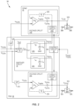
- FIG. 2 is a schematic diagram of an exemplary power management apparatus 36 configured according to another embodiment of the present disclosure to include a PMIC 38 and a distributed PMIC (DPMIC) 40 separated from the PMIC 38.
- DPMIC distributed PMIC
- the second voltage circuit 14B is instead provided in the DPMIC 40 that is physically separated from the PMIC 38 (e.g., in different dies).
- Such configuration can provide an increased flexibility as to where the first power amplifier circuit 28A and the second power amplifier circuit 28B can be provided in a wireless communication device (e.g., smart phone).
- the first power amplifier circuit 28A can be disposed close to an antenna(s) mounted on a top side of the wireless communication device, while the second power amplifier circuit 28B can be so disposed close to an antenna(s) mounted on a bottom side of the wireless communication device.
Landscapes
- Engineering & Computer Science (AREA)
- Power Engineering (AREA)
- Charge And Discharge Circuits For Batteries Or The Like (AREA)
- Inverter Devices (AREA)
- Dc-Dc Converters (AREA)
- Control Of Voltage And Current In General (AREA)
Claims (14)
- Leistungsverwaltungsvorrichtung (10), die Folgendes umfasst:
eine Switcher-Schaltung (16), die Folgendes umfasst:eine Multi-Level-Ladepumpe (MCP) (18), die so ausgebildet ist, dass sie auf der Basis eines Tastverhältnisses arbeitet, um eine Niederfrequenzspannung in Abhängigkeit von einer Batteriespannung zu erzeugen;eine erste Referenzspannungsschaltung (20A), die ausgebildet ist, eine erste Referenzspannung auf der Basis der Niederfrequenzspannung zu erzeugen; undeine zweite Referenzspannungsschaltung (20B), die ausgebildet ist, eine zweite Referenzspannung auf der Basis der Niederfrequenzspannung zu erzeugen;eine Steuerschaltung (22), die ausgebildet ist, um das Tastverhältnis auf der Basis einer ausgewählten ersten Zielspannung oder einer zweiten Zielspannung zu bestimmen, um dadurch die MCP (18) zu veranlassen, die Niederfrequenzspannung zu erzeugen;eine erste Spannungsschaltung (14A), die mit der ersten Referenzspannungsschaltung (20A) gekoppelt und ausgebildet ist, um eine erste modulierte Spannung zu erzeugen, indem sie eine erste modulierte Ausgangsspannung, die auf der Basis der ersten Zielspannung erzeugt wird, um eine erste Offset-Spannung erhöht, die auf der Basis der ersten Referenzspannung moduliert wird; undeine zweite Spannungsschaltung (14B), die mit der zweiten Referenzspannungsschaltung (20B) gekoppelt und ausgebildet ist, um eine zweite modulierte Spannung zu erzeugen, indem sie eine zweite modulierte Ausgangsspannung, die auf der Basis der zweiten Zielspannung erzeugt wird, um eine zweite Offset-Spannung erhöht, die auf der Basis der zweiten Referenzspannung moduliert wird. - Leistungsverwaltungsvorrichtung nach Anspruch 1, wobei die erste Referenzspannungsschaltung und die zweite Referenzspannungsschaltung jeweils dafür ausgebildet sind, eine der ersten und zweiten Referenzspannungen als Mittelwert der Niederfrequenzspannung zu erzeugen.
- Leistungsverwaltungsvorrichtung nach Anspruch 2, wobei es sich bei der ersten Referenzspannungsschaltung und der zweiten Referenzspannungsschaltung jeweils um eine Induktor-Kondensator-Schaltung (LC-Schaltung) handelt, die so ausgebildet ist, dass sie bei einer entsprechenden Resonanzfrequenz in Resonanz tritt, um die jeweilige erste Referenzspannung oder die zweite Referenzspannung als Mittelwert der Niederfrequenzspannung zu erzeugen.
- Leistungsverwaltungsvorrichtung nach Anspruch 2, wobei die erste Referenzspannung im Wesentlichen gleich der zweiten Referenzspannung ist.
- Leistungsverwaltungsvorrichtung nach Anspruch 1, wobei:
die erste Spannungsschaltung (14A) Folgendes umfasst:einen ersten Spannungsverstärker (VAa), der ausgebildet ist, um die erste modulierte Anfangsspannung auf der Basis der ersten Zielspannung zu erzeugen;einen ersten Offset-Kondensator (Coffa), der ausgebildet ist, um die erste modulierte Ausgangsspannung um die erste Offset-Spannung zu erhöhen, um die erste modulierte Spannung zu erzeugen; undeine erste Hybridschaltung (24A), die ausgebildet ist, um die erste Offset-Spannung auf der Basis der ersten Referenzspannung zu modulieren; undwobei die zweite Referenzspannungsschaltung (14B) Folgendes umfasst:einen zweiten Spannungsverstärker (VAb), der ausgebildet ist, um die zweite modulierte Anfangsspannung auf der Basis der zweiten Zielspannung zu erzeugen;einen zweiten Offset-Kondensator (Coffb), der ausgebildet ist, um die zweite modulierte Anfangsspannung um die zweite Offset-Spannung zu erhöhen, um die zweite modulierte Spannung zu erzeugen; undeine zweite Hybridschaltung (24B), die ausgebildet ist, um die zweite Offset-Spannung auf der Basis der zweiten Referenzspannung zu modulieren. - Leistungsverwaltungsvorrichtung nach Anspruch 5, wobei die erste Hybridschaltung und die zweite Hybridschaltung jeweils für Folgendes ausgebildet sind:Arbeiten in einem Schaltmodus, um zu veranlassen, dass die erste Offset-Spannung bzw. die zweite Offset-Spannung gleich der ersten Referenzspannung bzw. der zweiten Referenzspannung ist; undArbeiten in einem Low-Dropout-Modus (LDO), um zu veranlassen, dass die erste Offset-Spannung bzw. die zweite Offset-Spannung niedriger ist als die erste Referenzspannung bzw. die zweite Referenzspannung.
- Leistungsverwaltungsvorrichtung nach Anspruch 6, wobei die Steuerschaltung ferner ausgebildet ist, um die ausgewählte von der ersten Zielspannung und der zweiten Zielspannung als irgendeine von der ersten Zielspannung und der zweiten Zielspannung mit einem höheren Effektivwertpegel (RMS) zu bestimmen.
- Leistungsverwaltungsvorrichtung nach Anspruch 7, wobei die Steuerschaltung ferner für Folgendes ausgebildet ist:Bestimmen, dass die erste Zielspannung den höheren Effektivwert hat als die zweite Zielspannung;Veranlassen der MCP, die Niederfrequenzspannung auf der Basis der ersten Zielspannung zu erzeugen;Veranlassen der ersten Hybridschaltung, im Schaltmodus zu arbeiten; undVeranlassen der zweiten Hybridschaltung, im LDO-Modus zu arbeiten.
- Leistungsverwaltungsvorrichtung nach Anspruch 7, wobei die Steuerschaltung ferner für Folgendes ausgebildet ist:Bestimmen, dass die zweite Zielspannung den höheren Effektivwert hat als die erste Zielspannung;Veranlassen der MCP, die Niederfrequenzspannung auf der Basis der zweiten Zielspannung zu erzeugen;Veranlassen der ersten Hybridschaltung, im LDO-Modus zu arbeiten; undVeranlassen der zweiten Hybridschaltung, im Schaltmodus zu arbeiten.
- Leistungsverwaltungsvorrichtung nach Anspruch 7, wobei die Steuerschaltung ferner für Folgendes ausgebildet ist:Bestimmen, dass die erste Zielspannung und die zweite Zielspannung einen gleichen Effektivwert haben;Veranlassen der MCP, die Niederfrequenzspannung auf der Basis einer der ersten Zielspannung und der zweiten Zielspannung zu erzeugen;Veranlassen der ersten Hybridschaltung, im Schaltmodus zu arbeiten; undVeranlassen der zweiten Hybridschaltung, im Schaltmodus zu arbeiten.
- Leistungsverwaltungsvorrichtung nach Anspruch 1, die ferner eine integrierte Leistungsverwaltungsschaltung (PMIC) umfasst.
- Leistungsverwaltungsvorrichtung nach Anspruch 11, wobei die PMIC die erste Spannungsschaltung, die zweite Referenzspannungsschaltung, die Switcher-Schaltung und die Steuerschaltung umfasst.
- Leistungsverwaltungsvorrichtung nach Anspruch 11, wobei die PMIC die erste Spannungsschaltung, die Switcher-Schaltung und die Steuerschaltung umfasst.
- Leistungsverwaltungsvorrichtung nach Anspruch 13, die ferner eine verteilte PMIC umfasst, die von der PMIC getrennt ist und die zweite Referenzspannungsschaltung umfasst.
Priority Applications (1)
| Application Number | Priority Date | Filing Date | Title |
|---|---|---|---|
| EP24200740.9A EP4475434A3 (de) | 2020-12-22 | 2021-10-08 | Mit mehreren konfigurationen betreibbare leistungsverwaltungsvorrichtung |
Applications Claiming Priority (2)
| Application Number | Priority Date | Filing Date | Title |
|---|---|---|---|
| US202063128882P | 2020-12-22 | 2020-12-22 | |
| PCT/US2021/054141 WO2022139936A1 (en) | 2020-12-22 | 2021-10-08 | Power management apparatus operable with multiple configurations |
Related Child Applications (2)
| Application Number | Title | Priority Date | Filing Date |
|---|---|---|---|
| EP24200740.9A Division EP4475434A3 (de) | 2020-12-22 | 2021-10-08 | Mit mehreren konfigurationen betreibbare leistungsverwaltungsvorrichtung |
| EP24200740.9A Division-Into EP4475434A3 (de) | 2020-12-22 | 2021-10-08 | Mit mehreren konfigurationen betreibbare leistungsverwaltungsvorrichtung |
Publications (2)
| Publication Number | Publication Date |
|---|---|
| EP4268364A1 EP4268364A1 (de) | 2023-11-01 |
| EP4268364B1 true EP4268364B1 (de) | 2024-11-27 |
Family
ID=78592922
Family Applications (2)
| Application Number | Title | Priority Date | Filing Date |
|---|---|---|---|
| EP24200740.9A Pending EP4475434A3 (de) | 2020-12-22 | 2021-10-08 | Mit mehreren konfigurationen betreibbare leistungsverwaltungsvorrichtung |
| EP21806074.7A Active EP4268364B1 (de) | 2020-12-22 | 2021-10-08 | Mit mehreren konfigurationen betreibbare leistungsverwaltungsvorrichtung |
Family Applications Before (1)
| Application Number | Title | Priority Date | Filing Date |
|---|---|---|---|
| EP24200740.9A Pending EP4475434A3 (de) | 2020-12-22 | 2021-10-08 | Mit mehreren konfigurationen betreibbare leistungsverwaltungsvorrichtung |
Country Status (4)
| Country | Link |
|---|---|
| US (1) | US12212285B2 (de) |
| EP (2) | EP4475434A3 (de) |
| CN (1) | CN116686212A (de) |
| WO (1) | WO2022139936A1 (de) |
Families Citing this family (1)
| Publication number | Priority date | Publication date | Assignee | Title |
|---|---|---|---|---|
| CN121620847A (zh) * | 2023-08-28 | 2026-03-06 | Qorvo美国公司 | 功率管理电路中的无冲突电流分配 |
Citations (1)
| Publication number | Priority date | Publication date | Assignee | Title |
|---|---|---|---|---|
| US20200328720A1 (en) * | 2019-04-12 | 2020-10-15 | Qorvo Us, Inc. | Envelope tracking power amplifier apparatus |
Family Cites Families (322)
| Publication number | Priority date | Publication date | Assignee | Title |
|---|---|---|---|---|
| FR2558317B1 (fr) | 1984-01-13 | 1989-05-05 | Thomson Csf | Oscillateur accordable de grande precision et radar comportant un tel oscillateur |
| US5266936A (en) | 1989-05-09 | 1993-11-30 | Nec Corporation | Driving circuit for liquid crystal display |
| JPH0654877B2 (ja) | 1989-09-19 | 1994-07-20 | 日本電信電話株式会社 | 線形送信装置 |
| CA2109755C (en) | 1993-11-23 | 2004-11-02 | John Barry French | Composite bridge amplifier with output overload and thermal protection |
| US5838732A (en) | 1994-10-31 | 1998-11-17 | Airnet Communications Corp. | Reducing peak-to-average variance of a composite transmitted signal generated by a digital combiner via carrier phase offset |
| US6107862A (en) | 1997-02-28 | 2000-08-22 | Seiko Instruments Inc. | Charge pump circuit |
| US6141541A (en) | 1997-12-31 | 2000-10-31 | Motorola, Inc. | Method, device, phone and base station for providing envelope-following for variable envelope radio frequency signals |
| US6141377A (en) | 1998-07-30 | 2000-10-31 | Cisco Technology, Inc. | Method and apparatus for voice frequency noise reduction in splitterless ADSL |
| JP3630228B2 (ja) | 2000-08-16 | 2005-03-16 | インターナショナル・ビジネス・マシーンズ・コーポレーション | 電源供給装置、電池、電気機器、およびメモリ効果検出方法 |
| US6411531B1 (en) | 2000-11-21 | 2002-06-25 | Linear Technology Corporation | Charge pump DC/DC converters with reduced input noise |
| US7009858B2 (en) | 2001-01-29 | 2006-03-07 | Seiko Epson Corporation | Adjustable current consumption power supply apparatus |
| JP2002304434A (ja) | 2001-04-06 | 2002-10-18 | Nec Corp | Emiシミュレーション用半導体集積回路電源モデルの作成方法、装置及びプログラム |
| DE60134477D1 (de) | 2001-11-09 | 2008-07-31 | St Microelectronics Srl | Ladungspumpeschaltung mit niedriger Leistung |
| EP1573993B1 (de) | 2002-10-31 | 2010-01-13 | ZTE Corporation | Verfahren und system für breitband-vorverzerrungslinearisierung |
| US7432614B2 (en) | 2003-01-17 | 2008-10-07 | Hong Kong University Of Science And Technology | Single-inductor multiple-output switching converters in PCCM with freewheel switching |
| GB2398648B (en) | 2003-02-19 | 2005-11-09 | Nujira Ltd | Power supply stage for an amplifier |
| US6985033B1 (en) | 2003-05-15 | 2006-01-10 | Marvell International Ltd. | Circuits and methods for adjusting power amplifier predistortion, and power amplifiers and other devices including the same |
| US7043213B2 (en) | 2003-06-24 | 2006-05-09 | Northrop Grumman Corporation | Multi-mode amplifier system |
| US20050088160A1 (en) | 2003-09-19 | 2005-04-28 | Matsushita Electric Industrial Co., Ltd. | Multi output DC-DC converter |
| US7421254B2 (en) | 2003-10-23 | 2008-09-02 | Broadcom Corporation | High linearity, high efficiency power amplifier with DSP assisted linearity optimization |
| US7333582B2 (en) | 2004-03-02 | 2008-02-19 | Matsushita Electric Industrial Co., Ltd. | Two-point frequency modulation apparatus, wireless transmitting apparatus, and wireless receiving apparatus |
| US20050227646A1 (en) | 2004-03-18 | 2005-10-13 | Ryo Yamazaki | Detecting and maintaining linearity in a power amplifier system through comparing peak and RMS power levels |
| US7193467B2 (en) | 2004-03-30 | 2007-03-20 | Rambus Inc. | Differential amplifiers and methods of using same |
| US20060199553A1 (en) | 2005-03-07 | 2006-09-07 | Andrew Corporation | Integrated transceiver with envelope tracking |
| US7456621B2 (en) | 2005-05-06 | 2008-11-25 | Silicon Laboratories Inc. | Digital controller based power factor correction circuit |
| US20070053217A1 (en) | 2005-09-02 | 2007-03-08 | Lear Corporation | Converter for automotive use |
| JP2007074121A (ja) | 2005-09-05 | 2007-03-22 | Fujitsu Ltd | 増幅器及び相互コンダクタンス制御方法 |
| US7519336B2 (en) | 2006-05-05 | 2009-04-14 | Nokia Corporation | Method and arrangement for optimizing efficiency of a power amplifier |
| US7570931B2 (en) | 2006-06-02 | 2009-08-04 | Crestcom, Inc. | RF transmitter with variably biased RF power amplifier and method therefor |
| US7518445B2 (en) | 2006-06-04 | 2009-04-14 | Samsung Electro-Mechanics Company, Ltd. | Systems, methods, and apparatuses for linear envelope elimination and restoration transmitters |
| JP4369462B2 (ja) | 2006-11-22 | 2009-11-18 | Okiセミコンダクタ株式会社 | チャージポンプ型dc/dcコンバータ |
| US20080231115A1 (en) | 2007-03-16 | 2008-09-25 | Gyuha Cho | Multiple-Output DC-DC Converter |
| JP2008236683A (ja) | 2007-03-23 | 2008-10-02 | Mitsubishi Electric Corp | 電力増幅回路 |
| US7696735B2 (en) | 2007-03-30 | 2010-04-13 | Intel Corporation | Switched capacitor converters |
| US7471155B1 (en) | 2007-05-25 | 2008-12-30 | Rf Micro Devices, Inc. | Cancelling switching power supply ripple from a radio frequency signal |
| US7808220B2 (en) | 2007-07-11 | 2010-10-05 | Semtech Corporation | Method and apparatus for a charge pump DC-to-DC converter having parallel operating modes |
| US7949316B2 (en) | 2008-01-29 | 2011-05-24 | Panasonic Corporation | High-efficiency envelope tracking systems and methods for radio frequency power amplifiers |
| US20100019052A1 (en) | 2008-07-28 | 2010-01-28 | Yip Chiu Ming | Line voltage thermostat with energy measurement mechanism |
| US7859454B2 (en) | 2008-08-15 | 2010-12-28 | Broadcom Corporation | Method and system for calibrating group delay errors in a combined GPS and GLONASS receiver |
| US8463207B2 (en) | 2008-08-20 | 2013-06-11 | Freescale Semiconductor, Inc. | Wireless communication unit, integrated circuit and method of power control of a power amplifier therefor |
| JP5338262B2 (ja) | 2008-11-05 | 2013-11-13 | 日本電気株式会社 | 電力増幅器およびその増幅方法 |
| GB2530424B (en) | 2008-11-18 | 2016-05-04 | Nujira Ltd | Power Supply Arrangement For Multi-Stage Amplifier |
| JP6085406B2 (ja) | 2008-12-02 | 2017-02-22 | サイプレス セミコンダクター コーポレーション | 出力電圧制御回路、電子機器及び出力電圧制御方法 |
| US8232834B2 (en) | 2009-05-07 | 2012-07-31 | Analog Devices, Inc. | Boosting xDSL amplifier supply power on-demand |
| US8130042B2 (en) | 2009-06-03 | 2012-03-06 | Peregrine Semiconductor Corporation | Methods and devices for leakage current reduction |
| US8975879B2 (en) | 2009-09-14 | 2015-03-10 | Dialog Semiconductor Gmbh | Switching converter having a plurality N of outputs providing N output signals and at least one inductor and method for controlling such a switching converter |
| TWI422127B (zh) | 2009-09-29 | 2014-01-01 | Richtek Technology Corp | 升降壓式電源轉換器的控制電路及方法 |
| US8509713B2 (en) | 2009-12-21 | 2013-08-13 | Ubidyne, Inc. | Single envelope tracking system for an active antenna array |
| JP2011172206A (ja) | 2010-01-21 | 2011-09-01 | Panasonic Corp | 高周波電力増幅器及びそれを備える無線通信装置 |
| US8548398B2 (en) | 2010-02-01 | 2013-10-01 | Rf Micro Devices, Inc. | Envelope power supply calibration of a multi-mode radio frequency power amplifier |
| US7994862B1 (en) | 2010-02-11 | 2011-08-09 | Sige Semiconductor Inc. | Circuit and method of temperature dependent power amplifier biasing |
| GB2479579B (en) | 2010-04-15 | 2017-12-06 | Snaptrack Inc | Timing alignment for modulated supply |
| US8519788B2 (en) | 2010-04-19 | 2013-08-27 | Rf Micro Devices, Inc. | Boost charge-pump with fractional ratio and offset loop for supply modulation |
| WO2011133542A1 (en) | 2010-04-19 | 2011-10-27 | Rf Micro Devices, Inc. | Pseudo-envelope following power management system |
| US8942651B2 (en) | 2010-04-20 | 2015-01-27 | Rf Micro Devices, Inc. | Cascaded converged power amplifier |
| US9008597B2 (en) | 2010-04-20 | 2015-04-14 | Rf Micro Devices, Inc. | Direct current (DC)-DC converter having a multi-stage output filter |
| US9900204B2 (en) | 2010-04-20 | 2018-02-20 | Qorvo Us, Inc. | Multiple functional equivalence digital communications interface |
| US8731498B2 (en) | 2010-04-20 | 2014-05-20 | Rf Micro Devices, Inc. | Temperature correcting an envelope power supply signal for RF PA circuitry |
| US8706063B2 (en) | 2010-04-20 | 2014-04-22 | Rf Micro Devices, Inc. | PA envelope power supply undershoot compensation |
| US8174313B2 (en) | 2010-05-17 | 2012-05-08 | Avago Technologies Wireless Ip (Singapore) Pte. Ltd. | Apparatus and method for controlling power amplifier |
| GB2482738B (en) | 2010-08-13 | 2015-05-13 | Nujira Ltd | Switch mode power supply for envelope tracking |
| WO2012031241A2 (en) | 2010-09-03 | 2012-03-08 | Skyworks Solutions, Inc. | High-voltage tolerant voltage regulator |
| EP2432107B1 (de) | 2010-09-15 | 2013-10-23 | Nxp B.V. | Gleichspannungswandler mit einem Eingang und mehreren Ausgängen |
| US9172303B2 (en) | 2010-09-30 | 2015-10-27 | Stmicroelectronics International N.V. | Power management unit systems and methods |
| KR101743014B1 (ko) | 2010-11-11 | 2017-06-02 | 삼성전자주식회사 | 이동통신단말기의 출력 효율을 높이기 위한 장치 및 방법 |
| US8588713B2 (en) | 2011-01-10 | 2013-11-19 | Rf Micro Devices, Inc. | Power management system for multi-carriers transmitter |
| US8461928B2 (en) | 2011-01-25 | 2013-06-11 | Provigent Ltd. | Constant-gain power amplifier |
| US8803605B2 (en) | 2011-02-01 | 2014-08-12 | Mediatek Singapore Pte. Ltd. | Integrated circuit, wireless communication unit and method for providing a power supply |
| US9166538B2 (en) | 2011-02-01 | 2015-10-20 | Mediatek Singapore Pte. Ltd. | Integrated circuit wireless communication unit and method for providing a power supply |
| US8975960B2 (en) | 2011-02-01 | 2015-03-10 | Mediatek Singapore Pte. Ltd. | Integrated circuit wireless communication unit and method for providing a power supply |
| JP5996559B2 (ja) | 2011-02-07 | 2016-09-21 | スカイワークス ソリューションズ, インコーポレイテッドSkyworks Solutions, Inc. | 包絡線トラッキング較正のための装置および方法 |
| US8624760B2 (en) | 2011-02-07 | 2014-01-07 | Rf Micro Devices, Inc. | Apparatuses and methods for rate conversion and fractional delay calculation using a coefficient look up table |
| US8723492B2 (en) | 2011-03-22 | 2014-05-13 | Integrated Device Technology, Inc. | Autonomous controlled headroom low dropout regulator for single inductor multiple output power supply |
| US8725218B2 (en) | 2011-03-25 | 2014-05-13 | R2 Semiconductor, Inc. | Multimode operation DC-DC converter |
| US8718188B2 (en) | 2011-04-25 | 2014-05-06 | Skyworks Solutions, Inc. | Apparatus and methods for envelope tracking |
| EP2518878B1 (de) | 2011-04-29 | 2018-10-17 | STMicroelectronics S.r.l. | Gleichspannungswandler, Verfahren zum Betrieb des Gleichspannungswandlers, Umweltenergiegewinnungssystem mit dem Gleichspannungswandler und Vorrichtung mit dem System |
| US8774065B2 (en) | 2011-05-02 | 2014-07-08 | Rf Micro Devices, Inc. | Radio front end and power management architecture for LTE-advanced |
| US9379667B2 (en) | 2011-05-05 | 2016-06-28 | Rf Micro Devices, Inc. | Multiple power supply input parallel amplifier based envelope tracking |
| US9246460B2 (en) | 2011-05-05 | 2016-01-26 | Rf Micro Devices, Inc. | Power management architecture for modulated and constant supply operation |
| WO2012151594A2 (en) | 2011-05-05 | 2012-11-08 | Rf Micro Devices, Inc. | Power managent system for pseudo-envelope and average power tracking |
| US9247496B2 (en) | 2011-05-05 | 2016-01-26 | Rf Micro Devices, Inc. | Power loop control based envelope tracking |
| US9099919B2 (en) | 2011-05-09 | 2015-08-04 | The Hong Kong University Of Science And Technology | Single-inductor-multiple-output regulator with synchronized current mode hysteretic control |
| JP5637065B2 (ja) | 2011-05-13 | 2014-12-10 | 住友電気工業株式会社 | 増幅回路及び無線通信装置 |
| US8879665B2 (en) | 2011-06-08 | 2014-11-04 | Broadcom Corporation | Controlling a power amplifier based on transmitter output emissions |
| GB2488380B (en) | 2011-06-24 | 2018-04-04 | Snaptrack Inc | Envelope tracking system for mimo |
| US9065334B2 (en) | 2011-06-27 | 2015-06-23 | Mediatek Inc. | Voltage converter having auxiliary switch implemented therein and related voltage converting method thereof |
| US9496828B2 (en) | 2011-07-22 | 2016-11-15 | Texas Instruments Incorporated | System and method for envelope tracking power supply |
| US9018921B2 (en) | 2011-08-17 | 2015-04-28 | National Semiconductor Corporation | Battery charger architecture |
| US8699247B2 (en) | 2011-09-09 | 2014-04-15 | Sandisk Technologies Inc. | Charge pump system dynamically reconfigurable for read and program |
| KR101821294B1 (ko) | 2011-09-21 | 2018-01-23 | 삼성전자주식회사 | 감소된 대역폭 이티 및 디피디 처리장치 및 그 처리방법 |
| KR20130043425A (ko) | 2011-10-20 | 2013-04-30 | 삼성전자주식회사 | 입력 레벨에 따라 메모리 차수를 달리하는 디지털 전치 왜곡 방법 및 장치 |
| US8786371B2 (en) | 2011-11-18 | 2014-07-22 | Skyworks Solutions, Inc. | Apparatus and methods for voltage converters |
| US8868110B2 (en) | 2011-11-21 | 2014-10-21 | Broadcom Corporation | Wireless communication device capable of efficient network search |
| US9041364B2 (en) | 2011-12-01 | 2015-05-26 | Rf Micro Devices, Inc. | RF power converter |
| US9256234B2 (en) | 2011-12-01 | 2016-02-09 | Rf Micro Devices, Inc. | Voltage offset loop for a switching controller |
| US9041365B2 (en) | 2011-12-01 | 2015-05-26 | Rf Micro Devices, Inc. | Multiple mode RF power converter |
| US9280163B2 (en) | 2011-12-01 | 2016-03-08 | Rf Micro Devices, Inc. | Average power tracking controller |
| US8947161B2 (en) | 2011-12-01 | 2015-02-03 | Rf Micro Devices, Inc. | Linear amplifier power supply modulation for envelope tracking |
| WO2013084017A1 (en) | 2011-12-05 | 2013-06-13 | Freescale Semiconductor, Inc. | Self-bootstrap driving circuit and dc-dc converter |
| US8988054B2 (en) | 2011-12-27 | 2015-03-24 | St-Ericsson Sa | Single feedback loop for parallel architecture buck converter—LDO regulator |
| US9298198B2 (en) | 2011-12-28 | 2016-03-29 | Rf Micro Devices, Inc. | Noise reduction for envelope tracking |
| US20130176961A1 (en) | 2012-01-09 | 2013-07-11 | Qualcomm Incorporated | Apparatus and methods of unambiguous mac-i pdu formatting |
| GB2498392B (en) | 2012-01-16 | 2016-01-13 | Nujira Ltd | Crest factor reduction applied to shaping table to increase power amplifier efficency of envelope tracking amplifier |
| US8880012B2 (en) | 2012-01-19 | 2014-11-04 | Motorola Mobility Llc | Method and apparatus for resource block based transmitter optimization in wireless communication devices |
| KR101767577B1 (ko) | 2012-02-09 | 2017-08-23 | 스카이워크스 솔루션즈, 인코포레이티드 | 포락선 추적을 위한 장치 및 방법 |
| US9069365B2 (en) | 2012-02-18 | 2015-06-30 | R2 Semiconductor, Inc. | DC-DC converter enabling rapid output voltage changes |
| US9529375B2 (en) | 2012-02-28 | 2016-12-27 | Texas Instruments Deutschland Gmbh | Single inductor-multiple output DC-DC converter, method for operating the same and electronic device comprising the converter |
| CN104620509B (zh) | 2012-03-04 | 2017-05-10 | 匡坦斯公司 | 具有延迟校准的包络跟踪功率放大器系统及时间校准方法 |
| US20130234692A1 (en) | 2012-03-07 | 2013-09-12 | Medtronic, Inc. | Voltage supply and method with two references having differing accuracy and power consumption |
| JP5880239B2 (ja) | 2012-04-13 | 2016-03-08 | 株式会社ソシオネクスト | 電源装置及び電源の制御方法 |
| US8665016B2 (en) | 2012-04-30 | 2014-03-04 | Broadcom Corporation | Supply tracking |
| US8773200B2 (en) | 2012-07-08 | 2014-07-08 | R2 Semiconductor, Inc. | Decoupling circuits for filtering a voltage supply of multiple power amplifiers |
| US8896374B2 (en) | 2012-07-25 | 2014-11-25 | Qualcomm Incorporated | Energy source sharing |
| US9020451B2 (en) | 2012-07-26 | 2015-04-28 | Rf Micro Devices, Inc. | Programmable RF notch filter for envelope tracking |
| WO2014021318A1 (ja) | 2012-08-01 | 2014-02-06 | 独立行政法人産業技術総合研究所 | 音声分析合成のためのスペクトル包絡及び群遅延の推定システム及び音声信号の合成システム |
| US9473023B2 (en) | 2012-08-10 | 2016-10-18 | Texas Instruments Incorporated | Switched mode assisted linear regulator with seamless transition between power tracking configurations |
| US8884696B2 (en) | 2012-10-15 | 2014-11-11 | Intel Mobile Communications GmbH | Control circuit and method for controlling an operation of a power amplifier |
| WO2014060044A1 (en) | 2012-10-19 | 2014-04-24 | Telefonaktiebolaget L M Ericsson (Publ) | Apparatus and method for load modulating an amplifier |
| US9166536B2 (en) * | 2012-10-30 | 2015-10-20 | Eta Devices, Inc. | Transmitter architecture and related methods |
| US8818305B1 (en) | 2012-11-14 | 2014-08-26 | Motorola Mobility Llc | Supply transitions in an envelope tracked power amplifier |
| US9107167B2 (en) | 2012-12-03 | 2015-08-11 | Broadcom Corporation | Envelope tracking signal bandwidth control |
| US9167514B2 (en) | 2012-12-03 | 2015-10-20 | Broadcom Corporation | Unequal amplifier gain compression via shaping table |
| US9054643B2 (en) | 2012-12-19 | 2015-06-09 | Mediatek Singapore Pte. Ltd. | Method and apparatus for calibrating an envelope tracking system |
| US9219445B2 (en) | 2012-12-28 | 2015-12-22 | Peregrine Semiconductor Corporation | Optimization methods for amplifier with variable supply power |
| US11128261B2 (en) | 2012-12-28 | 2021-09-21 | Psemi Corporation | Constant Vds1 bias control for stacked transistor configuration |
| US9680434B2 (en) | 2012-12-28 | 2017-06-13 | Mediatek, Inc. | Method and apparatus for calibrating an envelope tracking system |
| US20140199949A1 (en) | 2013-01-16 | 2014-07-17 | Motorola Mobility Llc | Method for improving tx gain in envelope tracking systems |
| WO2014116933A2 (en) | 2013-01-24 | 2014-07-31 | Rf Micro Devices, Inc | Communications based adjustments of an envelope tracking power supply |
| US9306520B2 (en) | 2013-01-28 | 2016-04-05 | Qualcomm Incorporated | Reverse current prevention |
| US8824981B2 (en) | 2013-01-31 | 2014-09-02 | Intel Mobile Communications GmbH | Recalibration of envelope tracking transfer function during active transmission |
| GB2510395A (en) * | 2013-02-01 | 2014-08-06 | Nujira Ltd | Voltage supply stage for an envelope tracking modulated power supply |
| GB2511733B (en) | 2013-02-01 | 2020-08-19 | Snaptrack Inc | 2G support for 2G and 3G/4G envelope tracking modulator |
| US9263997B2 (en) | 2013-03-14 | 2016-02-16 | Quantance, Inc. | Self setting power supply using negative output impedance |
| CN105009449B (zh) | 2013-03-14 | 2017-08-08 | 匡坦斯公司 | 电源 |
| WO2014152903A2 (en) | 2013-03-14 | 2014-09-25 | Rf Micro Devices, Inc | Envelope tracking power supply voltage dynamic range reduction |
| EP2974005B1 (de) | 2013-03-14 | 2018-06-20 | Quantance, Inc. | Et-system mit rauschanpassung |
| WO2014151777A1 (en) | 2013-03-15 | 2014-09-25 | Quantance, Inc. | Envelope tracking system with internal power amplifier characterization |
| JP6107358B2 (ja) | 2013-04-17 | 2017-04-05 | 富士通株式会社 | 電源回路、電源ic、電力増幅装置および無線通信装置 |
| GB201309235D0 (en) | 2013-05-22 | 2013-07-03 | Nujira Ltd | Transfer function regulation |
| WO2014190505A1 (en) | 2013-05-29 | 2014-12-04 | Nokia Corporation | Amplification of a radio frequency signal |
| US9837962B2 (en) | 2013-06-06 | 2017-12-05 | Qualcomm Incorporated | Envelope tracker with variable boosted supply voltage |
| US10084376B2 (en) | 2013-06-13 | 2018-09-25 | Silicon Laboratories Inc. | Circuit with multiple output power converter |
| WO2015001851A1 (ja) | 2013-07-04 | 2015-01-08 | 株式会社村田製作所 | 電力増幅モジュール |
| US9166830B2 (en) | 2013-07-18 | 2015-10-20 | Intel Deutschland Gmbh | Systems and methods utilizing adaptive envelope tracking |
| US9356512B2 (en) | 2013-07-29 | 2016-05-31 | Broadcom Corporation | Envelope tracking power supply with direct connection to power source |
| US9088205B2 (en) | 2013-08-14 | 2015-07-21 | Quantance, Inc. | Stabilizing a power combining power supply system |
| CN104468437B (zh) | 2013-09-12 | 2017-11-14 | 富士通株式会社 | 数字预失真发射机及其控制方法 |
| KR20150040088A (ko) | 2013-10-04 | 2015-04-14 | 삼성전자주식회사 | 전력 증폭 장치 및 방법 |
| US9055529B2 (en) | 2013-10-04 | 2015-06-09 | Samsung Electronics Co., Ltd. | System and method for adaptive in-network time alignment for envelope tracking power amplifier |
| US9748845B1 (en) | 2013-11-02 | 2017-08-29 | Sridhar Kotikalapoodi | Method and apparatus for wide bandwidth, efficient power supply |
| US9397711B2 (en) | 2013-11-18 | 2016-07-19 | Qualcomm Incorporated | Pre-distortion in a wireless transmitter |
| US9231527B2 (en) | 2013-11-22 | 2016-01-05 | Qualcomm Incorporated | Circuits and methods for power amplification with extended high efficiency |
| US9362868B2 (en) | 2013-12-02 | 2016-06-07 | Futurewei Technologies, Inc. | Reduced power amplifier load impact for open loop envelope tracking |
| US9172330B2 (en) | 2013-12-02 | 2015-10-27 | Futurewei Technologies, Inc. | Nonlinear load pre-distortion for open loop envelope tracking |
| US9065509B1 (en) | 2014-01-09 | 2015-06-23 | Mediatek Inc. | Methods and apparatus for envelope tracking system |
| CN105981294B (zh) | 2014-02-10 | 2019-04-26 | 克莱尔瓦扬技术有限公司 | 用于rfid阅读器的极性发射机 |
| US20150236877A1 (en) | 2014-02-14 | 2015-08-20 | Mediatek Inc. | Methods and apparatus for envelope tracking system |
| US9520907B2 (en) | 2014-02-16 | 2016-12-13 | Mediatek Inc. | Methods and apparatus for envelope tracking system |
| KR101467231B1 (ko) | 2014-02-19 | 2014-12-01 | 성균관대학교산학협력단 | 포락선 추적 모드 또는 평균 전력 추적 모드로 동작하는 멀티 모드 바이어스 변조기 및 이를 이용한 포락선 추적 전력 증폭 장치 |
| US9203347B2 (en) | 2014-02-19 | 2015-12-01 | Futurewei Technologies, Inc. | Envelope tracking apparatus and method |
| US9203346B2 (en) | 2014-02-24 | 2015-12-01 | Futurewei Technologies, Inc. | Load current sensor for envelope tracking modulator |
| DE102014104364A1 (de) | 2014-03-28 | 2015-10-01 | Intel IP Corporation | Eine Vorrichtung und ein Verfahren zum Bereitstellen eines Versorgungssteuerungssignals für eine Versorgungseinheit |
| DE102014104371A1 (de) | 2014-03-28 | 2015-10-01 | Intel IP Corporation | Eine Vorrichtung und ein Verfahren zum Verstärken eines Sendesignals oder zum Bestimmenvon Werten eines Verzögerungssteuerungsparameters |
| KR20150115622A (ko) | 2014-04-04 | 2015-10-14 | 주식회사 엘지화학 | 헤테로고리 화합물 및 이를 포함하는 유기 발광 소자 |
| US20150311791A1 (en) | 2014-04-25 | 2015-10-29 | Taiwan Semiconductor Manufacturing Company Limited | Single inductor multiple output dc-dc convertor |
| US10333474B2 (en) | 2014-05-19 | 2019-06-25 | Skyworks Solutions, Inc. | RF transceiver front end module with improved linearity |
| US9768731B2 (en) * | 2014-07-23 | 2017-09-19 | Eta Devices, Inc. | Linearity and noise improvement for multilevel power amplifier systems using multi-pulse drain transitions |
| US9831834B2 (en) | 2014-07-29 | 2017-11-28 | Skyworks Solutions, Inc. | Envelope tracking with low frequency loss correction |
| US9445371B2 (en) | 2014-08-13 | 2016-09-13 | Skyworks Solutions, Inc. | Apparatus and methods for wideband envelope tracking systems |
| US9595981B2 (en) | 2014-08-26 | 2017-03-14 | Qorvo Us, Inc. | Reduced bandwidth envelope tracking |
| US9525384B2 (en) | 2014-09-02 | 2016-12-20 | Samsung Electronics Co., Ltd | Method and apparatus for supplying power to a radio frequency power amplifier |
| US9584071B2 (en) | 2014-10-03 | 2017-02-28 | Qorvo Us, Inc. | Envelope tracking with reduced dynamic range |
| EP3205006A1 (de) | 2014-10-06 | 2017-08-16 | IDT Europe GmbH | Gepulster linearer stromwandler |
| US9467095B2 (en) | 2014-10-13 | 2016-10-11 | Intel Corporation | Switchable dual core power amplifier |
| US9634620B2 (en) | 2014-12-05 | 2017-04-25 | Qorvo Us, Inc. | Envelope tracking with reduced circuit area and power consumption |
| US9692366B2 (en) | 2014-12-09 | 2017-06-27 | Intel Corporation | Envelope tracking path delay fine tuning and calibration |
| US9461590B2 (en) | 2014-12-12 | 2016-10-04 | Intel Corporation | Envelope tracking in connection with simultaneous transmission in one or more frequency bands |
| US9344304B1 (en) | 2014-12-18 | 2016-05-17 | Intel IP Corporation | Communication device with power supply load variation noise reduction for envelope tracking and method therefor |
| US9515622B2 (en) | 2014-12-23 | 2016-12-06 | Nokia Technologies Oy | Reconfigurable bias and supply drivers for radio frequency power amplifiers |
| DE102014119625A1 (de) | 2014-12-23 | 2016-06-23 | Intel IP Corporation | Schaltung und Verfahren zum Bereitstellen eines Radiofrequenzsignals |
| DE102014119479B4 (de) | 2014-12-23 | 2023-11-16 | Intel Corporation | Ein Push-Pull-Treiber, ein Sender, ein Empfänger, ein Sendeempfänger, eine integrierte Schaltung, ein Verfahren zum Erzeugen eines Signals an einem Ausgang |
| CN105739071B (zh) | 2014-12-24 | 2018-04-13 | 佳能株式会社 | 变焦镜头及包括该变焦镜头的摄像装置 |
| CN104539246B (zh) | 2015-01-04 | 2017-08-29 | 华为技术有限公司 | 基于包络跟踪的数字预畸变系统、射频系统和方法 |
| US9998241B2 (en) | 2015-02-19 | 2018-06-12 | Mediatek Inc. | Envelope tracking (ET) closed-loop on-the-fly calibration |
| EP3059858A1 (de) | 2015-02-23 | 2016-08-24 | Nokia Technologies OY | Verfahren und Vorrichtung für die Stromversorgung eines Verstärkers |
| US9595869B2 (en) | 2015-02-27 | 2017-03-14 | Qualcomm Incorporated | Multi-level switching regulator circuits and methods with finite state machine control |
| US9596110B2 (en) | 2015-04-02 | 2017-03-14 | Futurewei Technologies, Inc. | Open loop digital PWM envelope tracking system with dynamic boosting |
| WO2016195859A1 (en) | 2015-05-29 | 2016-12-08 | Rf Micro Devices, Inc. | Linear power amplifier |
| DE102015110238A1 (de) | 2015-06-25 | 2016-12-29 | Intel IP Corporation | Eine Schaltung und ein Verfahren zum Erzeugen eines Radiofrequenzsignals |
| US9948240B2 (en) | 2015-07-01 | 2018-04-17 | Qorvo Us, Inc. | Dual-output asynchronous power converter circuitry |
| US9912297B2 (en) * | 2015-07-01 | 2018-03-06 | Qorvo Us, Inc. | Envelope tracking power converter circuitry |
| US9800274B2 (en) | 2015-07-03 | 2017-10-24 | Mediatek, Inc. | Communication units and methods for power supply control |
| WO2017019803A1 (en) | 2015-07-28 | 2017-02-02 | Skyworks Solutions, Inc. | Power amplification system with programmable load line |
| NZ741164A (en) | 2015-09-08 | 2023-03-31 | Volt Tech Limited | Battery with a voltage regulation device |
| US10103693B2 (en) | 2015-09-30 | 2018-10-16 | Skyworks Solutions, Inc. | Power amplifier linearization system and method |
| US10116470B2 (en) | 2015-10-28 | 2018-10-30 | Futurewei Technologies, Inc. | Combined low and high frequency continuous-time linear equalizers |
| US10250194B2 (en) | 2015-11-13 | 2019-04-02 | Analog Devices Global | Broadband envelope tracking |
| CN106787716B (zh) | 2015-11-25 | 2020-09-15 | 恩智浦美国有限公司 | 单电感器多输出dc-dc转换器 |
| US10491003B2 (en) | 2015-12-23 | 2019-11-26 | Intel Corporation | Multiple input single inductor multiple output regulator |
| EP3386102B1 (de) | 2015-12-24 | 2021-03-31 | Huawei Technologies Co., Ltd. | Verfahren und vorrichtung zur steuerung eines leistungsverstärkers und system zur steuerung eines leistungsverstärkers |
| US9614477B1 (en) | 2016-01-12 | 2017-04-04 | Avago Technologies General Ip (Singapore) Pte. Ltd. | Envelope tracking supply modulators for multiple power amplifiers |
| US10382071B2 (en) | 2016-01-27 | 2019-08-13 | Qorvo Us, Inc. | Bandwidth optimization for power amplifier power supplies |
| KR102468952B1 (ko) | 2016-03-07 | 2022-11-22 | 삼성전자주식회사 | 신호를 송수신하는 전자 장치 및 방법 |
| JP6536466B2 (ja) | 2016-04-27 | 2019-07-03 | 株式会社オートネットワーク技術研究所 | 電源装置 |
| US9906428B2 (en) | 2016-04-28 | 2018-02-27 | Samsung Electronics Co., Ltd. | System and method for frequency-domain weighted least squares |
| US10181820B2 (en) | 2016-05-17 | 2019-01-15 | Skyworks Solutions, Inc. | Power amplification system with envelope-based bias |
| US9948350B2 (en) | 2016-07-06 | 2018-04-17 | Qorvo Us, Inc. | Multi-mode radio frequency circuitry |
| US10069470B2 (en) | 2016-08-12 | 2018-09-04 | Qorvo Us, Inc. | Multi-mode envelope tracking amplifier circuit |
| CN106208974A (zh) | 2016-08-30 | 2016-12-07 | 厦门信同信息技术有限公司 | 一种基于自适应数字包络跟踪技术的数字功率放大器的系统设计方法 |
| US10110169B2 (en) | 2016-09-14 | 2018-10-23 | Skyworks Solutions, Inc. | Apparatus and methods for envelope tracking systems with automatic mode selection |
| US9923520B1 (en) | 2016-09-21 | 2018-03-20 | Qualcomm Incorporated | Switching power supply for RF power amplifiers |
| CN109792205B (zh) | 2016-10-06 | 2020-10-30 | 株式会社村田制作所 | Dc-dc转换器 |
| US10243457B2 (en) | 2016-11-01 | 2019-03-26 | Lion Semiconductor Inc. | Feedback control for efficient high-speed battery charging |
| KR102678308B1 (ko) | 2016-11-02 | 2024-06-25 | 삼성전자주식회사 | 전원 변조기 및 이를 포함하는 통신 장치 |
| US10381983B2 (en) * | 2016-11-11 | 2019-08-13 | Skyworks Solutions, Inc. | Envelope tracking for high power amplifiers |
| KR102644277B1 (ko) * | 2016-11-25 | 2024-03-06 | 삼성전자주식회사 | 전원 변조기 및 이를 포함하는 통신 장치 |
| US10003416B1 (en) | 2016-12-16 | 2018-06-19 | Rohde & Schwarz Gmbh & Co. Kg | Method for measuring characteristics of a transmitter unit of a device under test, test system and radio frequency device |
| CN106877824A (zh) | 2016-12-29 | 2017-06-20 | 中国电子科技集团公司第五十研究所 | 基于fpga信号处理的包络跟踪电源控制系统及方法 |
| WO2018182778A1 (en) | 2017-03-30 | 2018-10-04 | Intel Corporation | Distributed feed-forward envelope tracking system |
| US10090808B1 (en) | 2017-03-30 | 2018-10-02 | Intel IP Corporation | Feed-forward envelope tracking |
| US10129823B2 (en) | 2017-03-31 | 2018-11-13 | Intel IP Corporation | Adaptive envelope tracking threshold |
| US10181826B2 (en) | 2017-04-25 | 2019-01-15 | Qorvo Us, Inc. | Envelope tracking amplifier circuit |
| TWI645277B (zh) | 2017-06-19 | 2018-12-21 | 瑞昱半導體股份有限公司 | 封包追蹤電源供應調控器 |
| US10615757B2 (en) | 2017-06-21 | 2020-04-07 | Skyworks Solutions, Inc. | Wide bandwidth envelope trackers |
| US10516368B2 (en) | 2017-06-21 | 2019-12-24 | Skyworks Solutions, Inc. | Fast envelope tracking systems for power amplifiers |
| US10158329B1 (en) | 2017-07-17 | 2018-12-18 | Qorvo Us, Inc. | Envelope tracking power amplifier circuit |
| US10158330B1 (en) | 2017-07-17 | 2018-12-18 | Qorvo Us, Inc. | Multi-mode envelope tracking amplifier circuit |
| US10284412B2 (en) | 2017-07-17 | 2019-05-07 | Qorvo Us, Inc. | Voltage memory digital pre-distortion circuit |
| KR102454811B1 (ko) | 2017-07-18 | 2022-10-13 | 삼성전기주식회사 | 옵셋 제거 기능이 개선된 엔벨로프-추적 전류 바이어스 회로 및 파워 증폭 장치 |
| US10090809B1 (en) | 2017-08-15 | 2018-10-02 | Qorvo Us, Inc. | Multi-mode mobile power management circuit |
| KR102163063B1 (ko) | 2017-08-30 | 2020-10-07 | 한국전자통신연구원 | Dc-dc 컨버터 구동 장치 및 이를 이용한 dc-dc 컨버터의 구동 방법 |
| US10326490B2 (en) | 2017-08-31 | 2019-06-18 | Qorvo Us, Inc. | Multi radio access technology power management circuit |
| US10326408B2 (en) | 2017-09-18 | 2019-06-18 | Qorvo Us, Inc. | Envelope tracking power management circuit |
| US20190103766A1 (en) | 2017-10-03 | 2019-04-04 | Qualcomm Incorporated | Multiple input single inductor multiple output (misimo) power conversion for power management circuits |
| US10530305B2 (en) | 2017-10-06 | 2020-01-07 | Qorvo Us, Inc. | Nonlinear bandwidth compression circuitry |
| US10097145B1 (en) | 2017-12-11 | 2018-10-09 | Qorvo Us, Inc. | Multi-mode power management circuit |
| US10361660B2 (en) | 2017-12-13 | 2019-07-23 | Qorvo Us, Inc. | Wide-bandwidth envelope tracking circuit |
| WO2019117933A1 (en) | 2017-12-15 | 2019-06-20 | Intel IP Corporation | Method and apparatus for digital envelope tracking with dynamically changing voltage levels for power amplifier |
| US10505454B2 (en) | 2017-12-22 | 2019-12-10 | Cirrus Logic, Inc. | Cross regulation reduction in single inductor multiple output (SIMO) switching DC-DC converters |
| US10439557B2 (en) | 2018-01-15 | 2019-10-08 | Qorvo Us, Inc. | Envelope tracking power management circuit |
| US10637408B2 (en) | 2018-01-18 | 2020-04-28 | Qorvo Us, Inc. | Envelope tracking voltage tracker circuit and related power management circuit |
| US10742170B2 (en) | 2018-02-01 | 2020-08-11 | Qorvo Us, Inc. | Envelope tracking circuit and related power amplifier system |
| KR102049350B1 (ko) | 2018-02-09 | 2019-11-27 | 성균관대학교산학협력단 | 이중 출력 및 이중 모드 서플라이 변조 장치, 이를 이용한 이단 전력 증폭기 그리고 그의 서플라이 변조 방법 |
| US10491175B2 (en) | 2018-02-28 | 2019-11-26 | Qorvo Us, Inc. | Power amplifier apparatus supporting reverse intermodulation product cancellation |
| US10361744B1 (en) | 2018-03-05 | 2019-07-23 | Qorvo Us, Inc. | Transceiver circuit and related radio frequency circuit |
| US10873260B2 (en) | 2018-03-12 | 2020-12-22 | Analog Devices International Unlimited Company | Zero-voltage switching hybrid switched-capacitor converter |
| US10476437B2 (en) | 2018-03-15 | 2019-11-12 | Qorvo Us, Inc. | Multimode voltage tracker circuit |
| US11063514B2 (en) | 2018-03-28 | 2021-07-13 | Qualcomm Incorporated | Methods and apparatuses for voltage regulation using predictively charged precharge rails |
| US10637399B2 (en) | 2018-04-17 | 2020-04-28 | Qorvo Us, Inc. | Low modulation bandwidth envelope tracking circuit |
| US10686407B2 (en) | 2018-04-30 | 2020-06-16 | Samsung Electronics Co., Ltd. | Symbol power tracking amplification system and a wireless communication device including the same |
| US10944365B2 (en) | 2018-06-28 | 2021-03-09 | Qorvo Us, Inc. | Envelope tracking amplifier circuit |
| KR20200010830A (ko) | 2018-07-23 | 2020-01-31 | 삼성전자주식회사 | 동적으로 출력 전압을 변경하는 스위칭 레귤레이터 및 이를 포함하는 전원 회로 |
| US10797650B2 (en) | 2018-07-24 | 2020-10-06 | Qorvo Us, Inc. | Envelope tracking amplifier apparatus |
| US10951183B2 (en) | 2018-09-13 | 2021-03-16 | Qorvo Us, Inc. | PA output memory neutralization using baseband I/O capacitance current compensation |
| US10911001B2 (en) | 2018-10-02 | 2021-02-02 | Qorvo Us, Inc. | Envelope tracking amplifier circuit |
| US10291126B1 (en) | 2018-10-18 | 2019-05-14 | BravoTek Electronics Co., Ltd. | Single-inductor multiple-output DC/DC converters with pulse-skipping mode and deadtime switch control |
| US10630375B1 (en) | 2018-10-19 | 2020-04-21 | Qorvo Us, Inc. | Envelope tracking amplifier apparatus |
| US11108359B2 (en) * | 2018-10-19 | 2021-08-31 | Qorvo Us, Inc. | Multi-amplifier envelope tracking circuit and related apparatus |
| US10931248B2 (en) | 2018-10-19 | 2021-02-23 | Qorvo Us, Inc. | Distributed envelope tracking amplifier circuit and related apparatus |
| US10985702B2 (en) | 2018-10-31 | 2021-04-20 | Qorvo Us, Inc. | Envelope tracking system |
| US11018638B2 (en) | 2018-10-31 | 2021-05-25 | Qorvo Us, Inc. | Multimode envelope tracking circuit and related apparatus |
| US10938351B2 (en) | 2018-10-31 | 2021-03-02 | Qorvo Us, Inc. | Envelope tracking system |
| US10680556B2 (en) | 2018-11-05 | 2020-06-09 | Qorvo Us, Inc. | Radio frequency front-end circuit |
| US10931245B2 (en) | 2018-11-12 | 2021-02-23 | Qorvo Us, Inc. | Radio frequency amplifier circuitry |
| US10756675B2 (en) | 2018-11-28 | 2020-08-25 | Qorvo Us, Inc. | Broadband power amplifier circuit |
| US11031909B2 (en) | 2018-12-04 | 2021-06-08 | Qorvo Us, Inc. | Group delay optimization circuit and related apparatus |
| KR102589640B1 (ko) | 2018-12-12 | 2023-10-16 | 삼성전자주식회사 | 컨버터 및 이를 포함한 회로 장치 |
| US11082007B2 (en) | 2018-12-19 | 2021-08-03 | Qorvo Us, Inc. | Envelope tracking integrated circuit and related apparatus |
| DE102019220150A1 (de) | 2018-12-19 | 2020-06-25 | Qorvo Us, Inc. | Integrierte Hüllkurvenverfolgungsschaltung und verwandte Vorrichtung |
| KR102067938B1 (ko) | 2019-01-14 | 2020-01-17 | 박천수 | 제로포스 이퀄라이징 벡터합성 앱솔루트 엔코더 구현방법 및 그 장치 |
| US11146213B2 (en) | 2019-01-15 | 2021-10-12 | Qorvo Us, Inc. | Multi-radio access technology envelope tracking amplifier apparatus |
| US11025458B2 (en) | 2019-02-07 | 2021-06-01 | Qorvo Us, Inc. | Adaptive frequency equalizer for wide modulation bandwidth envelope tracking |
| US10998859B2 (en) | 2019-02-07 | 2021-05-04 | Qorvo Us, Inc. | Dual-input envelope tracking integrated circuit and related apparatus |
| US11233481B2 (en) | 2019-02-18 | 2022-01-25 | Qorvo Us, Inc. | Modulated power apparatus |
| US11387797B2 (en) | 2019-03-15 | 2022-07-12 | Skyworks Solutions, Inc. | Envelope tracking systems for power amplifiers |
| US10790744B1 (en) | 2019-03-19 | 2020-09-29 | Analog Devices International Unlimited Company | Single inductor multiple output adaptive loop control |
| US11165393B2 (en) | 2019-03-25 | 2021-11-02 | Skyworks Solutions, Inc. | Envelope tracking for Doherty power amplifiers |
| US10855228B2 (en) | 2019-03-29 | 2020-12-01 | Intel Corporation | Voltage regulation systems and methods with adjustable boost and step-down regulation |
| US11374482B2 (en) | 2019-04-02 | 2022-06-28 | Qorvo Us, Inc. | Dual-modulation power management circuit |
| WO2020206246A1 (en) | 2019-04-03 | 2020-10-08 | Apple Inc. | DIGITAL ENVELOPE TRACKER FOR mmWAVE SYMBOL POWER TRACKING AND DIGITAL ENVELOPE TRACKER FOR MULTIPLE-TX CHANNELS WITH SHARED-RESOURCE VOLTAGE REGULATOR |
| US10978947B2 (en) | 2019-04-15 | 2021-04-13 | Qualcomm Incorporated | Single-inductor multiple-output (SIMO) power converter with a cross-regulation switch |
| US11018627B2 (en) | 2019-04-17 | 2021-05-25 | Qorvo Us, Inc. | Multi-bandwidth envelope tracking integrated circuit and related apparatus |
| US11424719B2 (en) | 2019-04-18 | 2022-08-23 | Qorvo Us, Inc. | Multi-bandwidth envelope tracking integrated circuit |
| US11139780B2 (en) * | 2019-04-24 | 2021-10-05 | Qorvo Us, Inc. | Envelope tracking apparatus |
| US11031911B2 (en) | 2019-05-02 | 2021-06-08 | Qorvo Us, Inc. | Envelope tracking integrated circuit and related apparatus |
| US10862431B1 (en) | 2019-05-30 | 2020-12-08 | Qorvo Us, Inc. | Envelope tracking amplification architecture |
| US11349436B2 (en) | 2019-05-30 | 2022-05-31 | Qorvo Us, Inc. | Envelope tracking integrated circuit |
| US11038464B2 (en) * | 2019-05-30 | 2021-06-15 | Qorvo Us, Inc. | Envelope tracking amplifier apparatus |
| US10622900B1 (en) | 2019-06-20 | 2020-04-14 | BravoTek Electronics Co., Ltd. | Single-inductor multiple-output DC-DC converter |
| WO2021016350A1 (en) | 2019-07-25 | 2021-01-28 | Qorvo Us, Inc. | Multi-mode power management apparatus |
| KR102751327B1 (ko) | 2019-08-01 | 2025-01-07 | 삼성전자주식회사 | 복수의 전압 레귤레이터들을 포함하는 전자 시스템 |
| US11539289B2 (en) | 2019-08-02 | 2022-12-27 | Qorvo Us, Inc. | Multi-level charge pump circuit |
| CN110492738B (zh) | 2019-08-08 | 2020-06-19 | 华南理工大学 | 一种单电感多输出dc-dc降压变换器 |
| US11637531B1 (en) | 2019-09-05 | 2023-04-25 | Murata Manufacturing Co., Ltd. | Supply generator and associated control methods |
| KR20250121144A (ko) | 2019-09-06 | 2025-08-11 | 에타 와이어리스, 아이엔씨. | 셀룰러 라디오용 밀리미터파 칩셋을 위한 전송 선로를 통한 전력 관리 제어 |
| GB2621260B (en) | 2019-09-27 | 2024-06-05 | Skyworks Solutions Inc | Multi-level envelope tracking systems with adjusted voltage steps |
| KR102928617B1 (ko) | 2019-11-26 | 2026-02-20 | 삼성전자 주식회사 | 복수의 리니어 레귤레이터를 이용하여 증폭기에 전압을 공급하는 방법 및 장치 |
| US11043959B1 (en) | 2019-12-06 | 2021-06-22 | Cirrus Logic, Inc. | Current digital-to-analog converter with warming of digital-to-analog converter elements |
| US11309922B2 (en) | 2019-12-13 | 2022-04-19 | Qorvo Us, Inc. | Multi-mode power management integrated circuit in a small formfactor wireless apparatus |
| US11271599B2 (en) | 2019-12-19 | 2022-03-08 | Qualcomm Incorporated | Envelope tracking system having fast transition time for a radio frequency (RF) amplifier |
| US11581855B2 (en) | 2019-12-20 | 2023-02-14 | Qorvo Us, Inc. | Power amplifier circuitry |
| US11349513B2 (en) | 2019-12-20 | 2022-05-31 | Qorvo Us, Inc. | Envelope tracking system |
| US11677365B2 (en) | 2020-01-08 | 2023-06-13 | Qorvo Us, Inc. | Envelope tracking power management apparatus incorporating multiple power amplifiers |
| US11539330B2 (en) | 2020-01-17 | 2022-12-27 | Qorvo Us, Inc. | Envelope tracking integrated circuit supporting multiple types of power amplifiers |
| US11716057B2 (en) | 2020-01-28 | 2023-08-01 | Qorvo Us, Inc. | Envelope tracking circuitry |
| US11677356B2 (en) | 2020-02-19 | 2023-06-13 | Samsung Electronics Co., Ltd. | Supply modulator and wireless communication apparatus including the same |
| US11728774B2 (en) | 2020-02-26 | 2023-08-15 | Qorvo Us, Inc. | Average power tracking power management integrated circuit |
| US11545945B2 (en) | 2020-03-04 | 2023-01-03 | Qorvo Us, Inc. | Apparatus and method for calibrating an envelope tracking lookup table |
| US11558016B2 (en) * | 2020-03-12 | 2023-01-17 | Qorvo Us, Inc. | Fast-switching average power tracking power management integrated circuit |
| US11196392B2 (en) | 2020-03-30 | 2021-12-07 | Qorvo Us, Inc. | Device and device protection system |
| US11258409B2 (en) | 2020-07-15 | 2022-02-22 | Qualcomm Incorporated | High voltage switch with fast turn-off |
| US12074514B2 (en) | 2020-09-18 | 2024-08-27 | Intel Corporation | Two stage multi-input multi-output regulator |
| US11909385B2 (en) | 2020-10-19 | 2024-02-20 | Qorvo Us, Inc. | Fast-switching power management circuit and related apparatus |
| JP2022067573A (ja) | 2020-10-20 | 2022-05-06 | 株式会社村田製作所 | 電力増幅回路 |
| WO2022103493A1 (en) | 2020-11-16 | 2022-05-19 | Qorvo Us, Inc. | Progressive envelope tracking with delay compensation |
| US12088263B2 (en) | 2021-01-08 | 2024-09-10 | Qorvo Us, Inc. | Equalizer circuit and related power management circuit |
| US12267046B2 (en) | 2021-02-15 | 2025-04-01 | Qorvo Us, Inc. | Power amplifier system |
| US12068720B2 (en) | 2021-02-26 | 2024-08-20 | Qorvo Us, Inc. | Barely Doherty dual envelope tracking (BD2E) circuit |
| US12212286B2 (en) | 2021-03-05 | 2025-01-28 | Qorvo Us, Inc. | Complementary envelope detector |
| US12126305B2 (en) | 2021-05-27 | 2024-10-22 | Qorvo Us, Inc. | Radio frequency (RF) equalizer in an envelope tracking (ET) circuit |
| US12063018B2 (en) | 2021-06-10 | 2024-08-13 | Qorvo Us, Inc. | Envelope tracking integrated circuit operable with multiple types of power amplifiers |
| US12007799B2 (en) | 2021-10-12 | 2024-06-11 | Everactive, Inc. | Energy operating systems and related techniques |
-
2021
- 2021-10-08 EP EP24200740.9A patent/EP4475434A3/de active Pending
- 2021-10-08 EP EP21806074.7A patent/EP4268364B1/de active Active
- 2021-10-08 WO PCT/US2021/054141 patent/WO2022139936A1/en not_active Ceased
- 2021-10-08 CN CN202180084068.0A patent/CN116686212A/zh active Pending
- 2021-10-08 US US18/039,805 patent/US12212285B2/en active Active
Patent Citations (1)
| Publication number | Priority date | Publication date | Assignee | Title |
|---|---|---|---|---|
| US20200328720A1 (en) * | 2019-04-12 | 2020-10-15 | Qorvo Us, Inc. | Envelope tracking power amplifier apparatus |
Also Published As
| Publication number | Publication date |
|---|---|
| EP4268364A1 (de) | 2023-11-01 |
| CN116686212A (zh) | 2023-09-01 |
| EP4475434A2 (de) | 2024-12-11 |
| EP4475434A3 (de) | 2025-03-05 |
| US20240030873A1 (en) | 2024-01-25 |
| WO2022139936A1 (en) | 2022-06-30 |
| US12212285B2 (en) | 2025-01-28 |
Similar Documents
| Publication | Publication Date | Title |
|---|---|---|
| US11146213B2 (en) | Multi-radio access technology envelope tracking amplifier apparatus | |
| US10630375B1 (en) | Envelope tracking amplifier apparatus | |
| US11018638B2 (en) | Multimode envelope tracking circuit and related apparatus | |
| US11906992B2 (en) | Distributed power management circuit | |
| US10103926B1 (en) | Multi-mode power management circuit | |
| US11677356B2 (en) | Supply modulator and wireless communication apparatus including the same | |
| EP4047817A1 (de) | Verteiltes leistungsverwaltungsgerät | |
| US11539289B2 (en) | Multi-level charge pump circuit | |
| US10044272B2 (en) | Supply modulator including switched-mode power supplier and transmitting device including the same | |
| US10992264B2 (en) | Envelope tracking circuit and related apparatus | |
| US20220200447A1 (en) | Fast-switching power management circuit operable to prolong battery life | |
| EP4268364B1 (de) | Mit mehreren konfigurationen betreibbare leistungsverwaltungsvorrichtung | |
| US20250023463A1 (en) | Multi-voltage power management integrated circuit | |
| US20120154687A1 (en) | Multi-band tunable antenna for integrated digital television service on mobile devices | |
| US20220360224A1 (en) | Supply voltage circuit for reducing in-rush battery current in an envelope tracking integrated circuit | |
| US12401279B2 (en) | Efficiency improvement in a power management integrated circuit | |
| US20240243708A1 (en) | Distributed power management circuit | |
| US12143067B2 (en) | Multi-transmission power management circuit | |
| US12249961B2 (en) | Wide bandwidth power amplifier apparatus | |
| US20250274043A1 (en) | Fast-switching power management integrated circuit | |
| US20230421105A1 (en) | Envelope tracking radio frequency front-end circuit | |
| HK40082306A (en) | Distributed power management circuit | |
| WO2024123410A1 (en) | Distributed power management circuit | |
| HK40075022A (en) | Distributed power management apparatus | |
| WO2022132460A1 (en) | Fast-switching power management circuit operable to prolong battery life |
Legal Events
| Date | Code | Title | Description |
|---|---|---|---|
| STAA | Information on the status of an ep patent application or granted ep patent |
Free format text: STATUS: UNKNOWN |
|
| STAA | Information on the status of an ep patent application or granted ep patent |
Free format text: STATUS: THE INTERNATIONAL PUBLICATION HAS BEEN MADE |
|
| PUAI | Public reference made under article 153(3) epc to a published international application that has entered the european phase |
Free format text: ORIGINAL CODE: 0009012 |
|
| STAA | Information on the status of an ep patent application or granted ep patent |
Free format text: STATUS: REQUEST FOR EXAMINATION WAS MADE |
|
| 17P | Request for examination filed |
Effective date: 20230717 |
|
| AK | Designated contracting states |
Kind code of ref document: A1 Designated state(s): AL AT BE BG CH CY CZ DE DK EE ES FI FR GB GR HR HU IE IS IT LI LT LU LV MC MK MT NL NO PL PT RO RS SE SI SK SM TR |
|
| DAV | Request for validation of the european patent (deleted) | ||
| DAX | Request for extension of the european patent (deleted) | ||
| GRAP | Despatch of communication of intention to grant a patent |
Free format text: ORIGINAL CODE: EPIDOSNIGR1 |
|
| STAA | Information on the status of an ep patent application or granted ep patent |
Free format text: STATUS: GRANT OF PATENT IS INTENDED |
|
| INTG | Intention to grant announced |
Effective date: 20240510 |
|
| GRAS | Grant fee paid |
Free format text: ORIGINAL CODE: EPIDOSNIGR3 |
|
| GRAA | (expected) grant |
Free format text: ORIGINAL CODE: 0009210 |
|
| STAA | Information on the status of an ep patent application or granted ep patent |
Free format text: STATUS: THE PATENT HAS BEEN GRANTED |
|
| AK | Designated contracting states |
Kind code of ref document: B1 Designated state(s): AL AT BE BG CH CY CZ DE DK EE ES FI FR GB GR HR HU IE IS IT LI LT LU LV MC MK MT NL NO PL PT RO RS SE SI SK SM TR |
|
| REG | Reference to a national code |
Ref country code: GB Ref legal event code: FG4D |
|
| REG | Reference to a national code |
Ref country code: CH Ref legal event code: EP |
|
| REG | Reference to a national code |
Ref country code: IE Ref legal event code: FG4D |
|
| REG | Reference to a national code |
Ref country code: DE Ref legal event code: R096 Ref document number: 602021022550 Country of ref document: DE |
|
| REG | Reference to a national code |
Ref country code: LT Ref legal event code: MG9D |
|
| REG | Reference to a national code |
Ref country code: NL Ref legal event code: MP Effective date: 20241127 |
|
| PG25 | Lapsed in a contracting state [announced via postgrant information from national office to epo] |
Ref country code: IS Free format text: LAPSE BECAUSE OF FAILURE TO SUBMIT A TRANSLATION OF THE DESCRIPTION OR TO PAY THE FEE WITHIN THE PRESCRIBED TIME-LIMIT Effective date: 20250327 Ref country code: HR Free format text: LAPSE BECAUSE OF FAILURE TO SUBMIT A TRANSLATION OF THE DESCRIPTION OR TO PAY THE FEE WITHIN THE PRESCRIBED TIME-LIMIT Effective date: 20241127 Ref country code: PT Free format text: LAPSE BECAUSE OF FAILURE TO SUBMIT A TRANSLATION OF THE DESCRIPTION OR TO PAY THE FEE WITHIN THE PRESCRIBED TIME-LIMIT Effective date: 20250327 |
|
| PG25 | Lapsed in a contracting state [announced via postgrant information from national office to epo] |
Ref country code: FI Free format text: LAPSE BECAUSE OF FAILURE TO SUBMIT A TRANSLATION OF THE DESCRIPTION OR TO PAY THE FEE WITHIN THE PRESCRIBED TIME-LIMIT Effective date: 20241127 Ref country code: NL Free format text: LAPSE BECAUSE OF FAILURE TO SUBMIT A TRANSLATION OF THE DESCRIPTION OR TO PAY THE FEE WITHIN THE PRESCRIBED TIME-LIMIT Effective date: 20241127 |
|
| REG | Reference to a national code |
Ref country code: AT Ref legal event code: MK05 Ref document number: 1746702 Country of ref document: AT Kind code of ref document: T Effective date: 20241127 |
|
| PG25 | Lapsed in a contracting state [announced via postgrant information from national office to epo] |
Ref country code: BG Free format text: LAPSE BECAUSE OF FAILURE TO SUBMIT A TRANSLATION OF THE DESCRIPTION OR TO PAY THE FEE WITHIN THE PRESCRIBED TIME-LIMIT Effective date: 20241127 |
|
| PG25 | Lapsed in a contracting state [announced via postgrant information from national office to epo] |
Ref country code: ES Free format text: LAPSE BECAUSE OF FAILURE TO SUBMIT A TRANSLATION OF THE DESCRIPTION OR TO PAY THE FEE WITHIN THE PRESCRIBED TIME-LIMIT Effective date: 20241127 |
|
| PG25 | Lapsed in a contracting state [announced via postgrant information from national office to epo] |
Ref country code: NO Free format text: LAPSE BECAUSE OF FAILURE TO SUBMIT A TRANSLATION OF THE DESCRIPTION OR TO PAY THE FEE WITHIN THE PRESCRIBED TIME-LIMIT Effective date: 20250227 |
|
| PG25 | Lapsed in a contracting state [announced via postgrant information from national office to epo] |
Ref country code: AT Free format text: LAPSE BECAUSE OF FAILURE TO SUBMIT A TRANSLATION OF THE DESCRIPTION OR TO PAY THE FEE WITHIN THE PRESCRIBED TIME-LIMIT Effective date: 20241127 Ref country code: LV Free format text: LAPSE BECAUSE OF FAILURE TO SUBMIT A TRANSLATION OF THE DESCRIPTION OR TO PAY THE FEE WITHIN THE PRESCRIBED TIME-LIMIT Effective date: 20241127 Ref country code: GR Free format text: LAPSE BECAUSE OF FAILURE TO SUBMIT A TRANSLATION OF THE DESCRIPTION OR TO PAY THE FEE WITHIN THE PRESCRIBED TIME-LIMIT Effective date: 20250228 |
|
| PG25 | Lapsed in a contracting state [announced via postgrant information from national office to epo] |
Ref country code: PL Free format text: LAPSE BECAUSE OF FAILURE TO SUBMIT A TRANSLATION OF THE DESCRIPTION OR TO PAY THE FEE WITHIN THE PRESCRIBED TIME-LIMIT Effective date: 20241127 |
|
| PG25 | Lapsed in a contracting state [announced via postgrant information from national office to epo] |
Ref country code: RS Free format text: LAPSE BECAUSE OF FAILURE TO SUBMIT A TRANSLATION OF THE DESCRIPTION OR TO PAY THE FEE WITHIN THE PRESCRIBED TIME-LIMIT Effective date: 20250227 |
|
| PG25 | Lapsed in a contracting state [announced via postgrant information from national office to epo] |
Ref country code: SM Free format text: LAPSE BECAUSE OF FAILURE TO SUBMIT A TRANSLATION OF THE DESCRIPTION OR TO PAY THE FEE WITHIN THE PRESCRIBED TIME-LIMIT Effective date: 20241127 |
|
| PG25 | Lapsed in a contracting state [announced via postgrant information from national office to epo] |
Ref country code: DK Free format text: LAPSE BECAUSE OF FAILURE TO SUBMIT A TRANSLATION OF THE DESCRIPTION OR TO PAY THE FEE WITHIN THE PRESCRIBED TIME-LIMIT Effective date: 20241127 |
|
| PG25 | Lapsed in a contracting state [announced via postgrant information from national office to epo] |
Ref country code: EE Free format text: LAPSE BECAUSE OF FAILURE TO SUBMIT A TRANSLATION OF THE DESCRIPTION OR TO PAY THE FEE WITHIN THE PRESCRIBED TIME-LIMIT Effective date: 20241127 |
|
| PG25 | Lapsed in a contracting state [announced via postgrant information from national office to epo] |
Ref country code: RO Free format text: LAPSE BECAUSE OF FAILURE TO SUBMIT A TRANSLATION OF THE DESCRIPTION OR TO PAY THE FEE WITHIN THE PRESCRIBED TIME-LIMIT Effective date: 20241127 |
|
| PG25 | Lapsed in a contracting state [announced via postgrant information from national office to epo] |
Ref country code: SK Free format text: LAPSE BECAUSE OF FAILURE TO SUBMIT A TRANSLATION OF THE DESCRIPTION OR TO PAY THE FEE WITHIN THE PRESCRIBED TIME-LIMIT Effective date: 20241127 |
|
| PG25 | Lapsed in a contracting state [announced via postgrant information from national office to epo] |
Ref country code: CZ Free format text: LAPSE BECAUSE OF FAILURE TO SUBMIT A TRANSLATION OF THE DESCRIPTION OR TO PAY THE FEE WITHIN THE PRESCRIBED TIME-LIMIT Effective date: 20241127 |
|
| PG25 | Lapsed in a contracting state [announced via postgrant information from national office to epo] |
Ref country code: IT Free format text: LAPSE BECAUSE OF FAILURE TO SUBMIT A TRANSLATION OF THE DESCRIPTION OR TO PAY THE FEE WITHIN THE PRESCRIBED TIME-LIMIT Effective date: 20241127 |
|
| REG | Reference to a national code |
Ref country code: DE Ref legal event code: R097 Ref document number: 602021022550 Country of ref document: DE |
|
| PG25 | Lapsed in a contracting state [announced via postgrant information from national office to epo] |
Ref country code: SE Free format text: LAPSE BECAUSE OF FAILURE TO SUBMIT A TRANSLATION OF THE DESCRIPTION OR TO PAY THE FEE WITHIN THE PRESCRIBED TIME-LIMIT Effective date: 20241127 |
|
| PLBE | No opposition filed within time limit |
Free format text: ORIGINAL CODE: 0009261 |
|
| STAA | Information on the status of an ep patent application or granted ep patent |
Free format text: STATUS: NO OPPOSITION FILED WITHIN TIME LIMIT |
|
| PGFP | Annual fee paid to national office [announced via postgrant information from national office to epo] |
Ref country code: GB Payment date: 20250923 Year of fee payment: 5 |
|
| PGFP | Annual fee paid to national office [announced via postgrant information from national office to epo] |
Ref country code: FR Payment date: 20250923 Year of fee payment: 5 |
|
| 26N | No opposition filed |
Effective date: 20250828 |
|
| P01 | Opt-out of the competence of the unified patent court (upc) registered |
Free format text: CASE NUMBER: UPC_APP_8123_4268364/2025 Effective date: 20250926 |
|
| PGFP | Annual fee paid to national office [announced via postgrant information from national office to epo] |
Ref country code: DE Payment date: 20250923 Year of fee payment: 5 |