EP4236653A2 - Anzeigevorrichtung - Google Patents
Anzeigevorrichtung Download PDFInfo
- Publication number
- EP4236653A2 EP4236653A2 EP23178795.3A EP23178795A EP4236653A2 EP 4236653 A2 EP4236653 A2 EP 4236653A2 EP 23178795 A EP23178795 A EP 23178795A EP 4236653 A2 EP4236653 A2 EP 4236653A2
- Authority
- EP
- European Patent Office
- Prior art keywords
- pad
- film
- electrode
- display device
- touch
- Prior art date
- Legal status (The legal status is an assumption and is not a legal conclusion. Google has not performed a legal analysis and makes no representation as to the accuracy of the status listed.)
- Pending
Links
Images


Classifications
-
- H—ELECTRICITY
- H10—SEMICONDUCTOR DEVICES; ELECTRIC SOLID-STATE DEVICES NOT OTHERWISE PROVIDED FOR
- H10K—ORGANIC ELECTRIC SOLID-STATE DEVICES
- H10K59/00—Integrated devices, or assemblies of multiple devices, comprising at least one organic light-emitting element covered by group H10K50/00
- H10K59/40—OLEDs integrated with touch screens
-
- G—PHYSICS
- G06—COMPUTING OR CALCULATING; COUNTING
- G06F—ELECTRIC DIGITAL DATA PROCESSING
- G06F3/00—Input arrangements for transferring data to be processed into a form capable of being handled by the computer; Output arrangements for transferring data from processing unit to output unit, e.g. interface arrangements
- G06F3/01—Input arrangements or combined input and output arrangements for interaction between user and computer
- G06F3/03—Arrangements for converting the position or the displacement of a member into a coded form
- G06F3/041—Digitisers, e.g. for touch screens or touch pads, characterised by the transducing means
- G06F3/0412—Digitisers structurally integrated in a display
-
- G—PHYSICS
- G06—COMPUTING OR CALCULATING; COUNTING
- G06F—ELECTRIC DIGITAL DATA PROCESSING
- G06F3/00—Input arrangements for transferring data to be processed into a form capable of being handled by the computer; Output arrangements for transferring data from processing unit to output unit, e.g. interface arrangements
- G06F3/01—Input arrangements or combined input and output arrangements for interaction between user and computer
- G06F3/03—Arrangements for converting the position or the displacement of a member into a coded form
- G06F3/041—Digitisers, e.g. for touch screens or touch pads, characterised by the transducing means
- G06F3/0416—Control or interface arrangements specially adapted for digitisers
- G06F3/04164—Connections between sensors and controllers, e.g. routing lines between electrodes and connection pads
-
- G—PHYSICS
- G06—COMPUTING OR CALCULATING; COUNTING
- G06F—ELECTRIC DIGITAL DATA PROCESSING
- G06F3/00—Input arrangements for transferring data to be processed into a form capable of being handled by the computer; Output arrangements for transferring data from processing unit to output unit, e.g. interface arrangements
- G06F3/01—Input arrangements or combined input and output arrangements for interaction between user and computer
- G06F3/03—Arrangements for converting the position or the displacement of a member into a coded form
- G06F3/041—Digitisers, e.g. for touch screens or touch pads, characterised by the transducing means
- G06F3/044—Digitisers, e.g. for touch screens or touch pads, characterised by the transducing means by capacitive means
- G06F3/0443—Digitisers, e.g. for touch screens or touch pads, characterised by the transducing means by capacitive means using a single layer of sensing electrodes
-
- G—PHYSICS
- G06—COMPUTING OR CALCULATING; COUNTING
- G06F—ELECTRIC DIGITAL DATA PROCESSING
- G06F3/00—Input arrangements for transferring data to be processed into a form capable of being handled by the computer; Output arrangements for transferring data from processing unit to output unit, e.g. interface arrangements
- G06F3/01—Input arrangements or combined input and output arrangements for interaction between user and computer
- G06F3/03—Arrangements for converting the position or the displacement of a member into a coded form
- G06F3/041—Digitisers, e.g. for touch screens or touch pads, characterised by the transducing means
- G06F3/044—Digitisers, e.g. for touch screens or touch pads, characterised by the transducing means by capacitive means
- G06F3/0446—Digitisers, e.g. for touch screens or touch pads, characterised by the transducing means by capacitive means using a grid-like structure of electrodes in at least two directions, e.g. using row and column electrodes
-
- H—ELECTRICITY
- H10—SEMICONDUCTOR DEVICES; ELECTRIC SOLID-STATE DEVICES NOT OTHERWISE PROVIDED FOR
- H10K—ORGANIC ELECTRIC SOLID-STATE DEVICES
- H10K50/00—Organic light-emitting devices
- H10K50/80—Constructional details
- H10K50/84—Passivation; Containers; Encapsulations
- H10K50/844—Encapsulations
-
- H—ELECTRICITY
- H10—SEMICONDUCTOR DEVICES; ELECTRIC SOLID-STATE DEVICES NOT OTHERWISE PROVIDED FOR
- H10K—ORGANIC ELECTRIC SOLID-STATE DEVICES
- H10K50/00—Organic light-emitting devices
- H10K50/80—Constructional details
- H10K50/86—Arrangements for improving contrast, e.g. preventing reflection of ambient light
- H10K50/865—Arrangements for improving contrast, e.g. preventing reflection of ambient light comprising light absorbing layers, e.g. light-blocking layers
-
- H—ELECTRICITY
- H10—SEMICONDUCTOR DEVICES; ELECTRIC SOLID-STATE DEVICES NOT OTHERWISE PROVIDED FOR
- H10K—ORGANIC ELECTRIC SOLID-STATE DEVICES
- H10K59/00—Integrated devices, or assemblies of multiple devices, comprising at least one organic light-emitting element covered by group H10K50/00
- H10K59/10—OLED displays
- H10K59/12—Active-matrix OLED [AMOLED] displays
- H10K59/122—Pixel-defining structures or layers, e.g. banks
-
- H—ELECTRICITY
- H10—SEMICONDUCTOR DEVICES; ELECTRIC SOLID-STATE DEVICES NOT OTHERWISE PROVIDED FOR
- H10K—ORGANIC ELECTRIC SOLID-STATE DEVICES
- H10K59/00—Integrated devices, or assemblies of multiple devices, comprising at least one organic light-emitting element covered by group H10K50/00
- H10K59/10—OLED displays
- H10K59/12—Active-matrix OLED [AMOLED] displays
- H10K59/124—Insulating layers formed between TFT elements and OLED elements
-
- H—ELECTRICITY
- H10—SEMICONDUCTOR DEVICES; ELECTRIC SOLID-STATE DEVICES NOT OTHERWISE PROVIDED FOR
- H10K—ORGANIC ELECTRIC SOLID-STATE DEVICES
- H10K59/00—Integrated devices, or assemblies of multiple devices, comprising at least one organic light-emitting element covered by group H10K50/00
- H10K59/10—OLED displays
- H10K59/12—Active-matrix OLED [AMOLED] displays
- H10K59/131—Interconnections, e.g. wiring lines or terminals
-
- H—ELECTRICITY
- H10—SEMICONDUCTOR DEVICES; ELECTRIC SOLID-STATE DEVICES NOT OTHERWISE PROVIDED FOR
- H10K—ORGANIC ELECTRIC SOLID-STATE DEVICES
- H10K59/00—Integrated devices, or assemblies of multiple devices, comprising at least one organic light-emitting element covered by group H10K50/00
- H10K59/30—Devices specially adapted for multicolour light emission
- H10K59/35—Devices specially adapted for multicolour light emission comprising red-green-blue [RGB] subpixels
-
- H—ELECTRICITY
- H10—SEMICONDUCTOR DEVICES; ELECTRIC SOLID-STATE DEVICES NOT OTHERWISE PROVIDED FOR
- H10K—ORGANIC ELECTRIC SOLID-STATE DEVICES
- H10K59/00—Integrated devices, or assemblies of multiple devices, comprising at least one organic light-emitting element covered by group H10K50/00
- H10K59/80—Constructional details
- H10K59/805—Electrodes
-
- H—ELECTRICITY
- H10—SEMICONDUCTOR DEVICES; ELECTRIC SOLID-STATE DEVICES NOT OTHERWISE PROVIDED FOR
- H10K—ORGANIC ELECTRIC SOLID-STATE DEVICES
- H10K59/00—Integrated devices, or assemblies of multiple devices, comprising at least one organic light-emitting element covered by group H10K50/00
- H10K59/80—Constructional details
- H10K59/87—Passivation; Containers; Encapsulations
- H10K59/873—Encapsulations
- H10K59/8731—Encapsulations multilayered coatings having a repetitive structure, e.g. having multiple organic-inorganic bilayers
Definitions
- the present disclosure relates to a display device and a method of manufacturing the same.
- LCD liquid crystal display
- PDP plasma display panel
- OLED organic light emitting display
- the organic light emitting display device is a self-light emitting device, and has advantages in that a viewing angle and a contrast ratio are more excellent than those of the liquid crystal display (LCD) device. Also, since the organic light emitting display device does not require a separate backlight, it is advantageous that the organic light emitting display device is able to be thin and lightweight and has low power consumption. Furthermore, the organic light emitting display device has advantages in that it may be driven at a low direct current voltage, has a fast response speed, and especially has a low manufacturing cost.
- LCD liquid crystal display
- the organic light emitting display device includes pixels, each of which includes an organic light emitting diode, and has a disadvantage in that the organic light emitting diode may be easily degraded by external factors such as external water and oxygen. In order to prevent this, the organic light emitting display device forms an encapsulation film to prevent external water and oxygen from being permeated into the organic light emitting diode.
- the encapsulation film includes at least one inorganic film and at least one organic film to prevent oxygen or water from being permeated into an organic light emitting layer and an electrode.
- at least one organic film generally includes a polymer, and is formed by a hardening process after being doped on a substrate in a liquid type. Since such an organic film has flexibility until the hardening process is performed, a problem may occur in that the organic film may overflow outside an area where the encapsulation film is to be formed. For example, the organic film may overflow toward a pad area where a plurality of pads are provided. To solve this problem, a dam for blocking a flow of the organic film is formed along the outside of the organic light emitting diode.
- At least one inorganic film is entirely formed on the organic light emitting diode except a pad area where a pad electrode is arranged.
- a mask for covering the pad electrode is arranged on the pad electrode, and then the inorganic film is formed.
- the mask is arranged to be close to the pad electrode such that the inorganic film is not formed in the pad area. At this time, arcing may occur between a boundary surface of the mask for covering the pad area and the pad electrode. If arcing occurs between the mask and the pad electrode, a high current entering the pad electrode from the mask may flow into the display device along the pad electrode, whereby a defect may occur.
- the present disclosure is directed to a display device and a method of manufacturing the same, which substantially obviate one or more problems due to limitations and disadvantages of the related art.
- An object of the present disclosure may be to provide a display device and a method of manufacturing the same in which arcing may be prevented from occurring.
- the present disclosure provides a display device and a method of manufacturing the same, wherein the display device comprises a first substrate including a display area on which pixels are arranged, and a non-display area surrounding the display area; a dam surrounding the display area, arranged on the non-display area; a pad electrode arranged outside the dam; and an encapsulation film covering the display area and including a first inorganic film, wherein the first inorganic film surrounds or at least partially covers the pad electrode.
- first element is positioned "on or above” a second element, or “over” a second element, it should be understood that the first and second elements may be brought into contact with each other, or a third element may be interposed between the first and second elements.
- FIG. 1 is a perspective view illustrating a display device according to one example of the present disclosure.
- FIG. 2 is a block view illustrating a display device according to one example of the present disclosure.
- the display device includes a display panel 110, a scan driver 120, a data driver 130, a timing controller 160, a host system 170, a touch driver 180, and a touch coordinate calculator 190.
- the display device with a built-in touch screen according to the example of the present disclosure may be realized as a flat panel display device such as a Liquid Crystal Display (LCD), Field Emission Display (FED), Plasma Display Panel (PDP), Organic Light Emitting Display (OLED), and Electrophoresis display (EPD).
- LCD Liquid Crystal Display
- FED Field Emission Display
- PDP Plasma Display Panel
- OLED Organic Light Emitting Display
- EPD Electrophoresis display
- the display device with a built-in touch screen according to the example of the present disclosure is realized as, but not limited to, an organic light emitting display device.
- the display panel 110 includes a display area on which pixels P are arranged to display an image.
- data lines D1 to Dm (m is a positive integer of 2 or more) and scan lines S1 to Sn (n is a positive integer of 2 or more) are provided.
- the data lines D1 to Dm may be formed to cross the scan lines S1 to Sn.
- the pixels P may be formed on the area defined by a crossed structure of the gate lines and data lines.
- Each of the pixels P of the display panel 110 may be connected to any one of the data lines D1 to Dm and any one of the scan lines S1 to Sn.
- Each of the pixels P of the display panel 110 may include a driving transistor for controlling a drain-source current in accordance with a data voltage applied to a gate electrode, a scan transistor turned on by a scan signal of the scan line, supplying a data voltage of the data line to the gate electrode of the driving transistor, an organic light emitting diode for emitting light in accordance with the drain-source current of the driving transistor, and a capacitor for storing a voltage of the gate electrode of the driving transistor. Therefore, each of the pixels P may emit light in accordance with the current supplied to the organic light emitting diode.
- the scan driver 120 receives a scan control signal GCS from the timing controller 160.
- the scan driver 120 supplies scan signals to the scan lines S1 ⁇ Sn in accordance with the scan control signal GCS.
- the scan driver 120 may be formed in a non-display area outside one side or both sides of a display area of the display panel 110 in a GIP (gate driver in panel) mode.
- the scan driver 120 is fabricated of a driving chip, packaged in a flexible film, and may be attached to the non-display area outside one side or both sides of the display area of the display panel 110 in a TAB (tape automated bonding) mode.
- the data driver 130 receives digital video data DATA and a data control signal DCS from the timing controller 160.
- the data driver 130 converts the digital video data DATA into an analogue positive polarity/negative polarity data voltage in accordance with the data control signal DCS and supplies them to the data lines. That is, pixels to which the data voltages will be supplied are selected by the scan signals of the scan driver 120, and the data voltages are supplied to the selected pixels.
- the data driver 130 may include a plurality of source drive ICs.
- Each of the plurality of source drive ICs may be packaged into the flexible film 140 in a COF (chip on film) or COP (chip on plastic) mode.
- the flexible film 140 is attached onto pads provided on the non-display area of the display panel 110 using an anisotropic conducting film, whereby the source drive ICs may be connected to the pads.
- the circuit board 150 may be attached to the flexible films 140.
- a plurality of circuits realized as driving chips may be packaged onto the circuit board 150.
- the timing controller 160 may be packaged onto the circuit board 150.
- the circuit board 150 may be a printed circuit board or flexible printed circuit board.
- the timing controller 160 receives digital video data DATA and timing signals from the host system 170.
- the timing signals may include a vertical synchronization signal, a horizontal synchronization signal, a data enable signal, and a dot clock.
- the vertical synchronization signal is a signal defining one frame period.
- the horizontal synchronization signal is a signal defining one horizontal period needed to supply the data voltages to pixels of one horizontal line of the display panel DIS.
- the data enable signal is a signal for defining a period of inputting available data.
- the dot clock is a signal repeated with a predetermined short period.
- the timing controller 160 In order to control operation timings of the scan driver 120 and the data driver 130, the timing controller 160 generates a data control signal DCS to control operation timing of the data driver 130 and a scan control signal GCS for controlling operation timing of the data driver 130 based on the timing signals.
- the timing controller 160 outputs the scan control signal GCS to the scan driver 120 and outputs the digital video data DATA and the data control signal DCS to the data driver 130.
- the host system 170 may be realized as a navigation system, a set-top box, a DVD player, a blue-ray player, a personal computer (PC), a home theater system, a broadcasting receiver, and a phone system.
- the host system 170 includes SoC (System on chip) equipped with a scaler and converts the digital video data DATA of an input image to a format suitable to display the display panel 110.
- SoC System on chip
- the host system 170 transmits the digital video data DATA and the timing signals to the timing controller 160.
- first and the second touch electrodes may be formed on the display panel 110.
- the first touch electrodes may be formed to cross the second touch electrodes.
- the first touch electrodes may be connected to a first touch driver 181 through first touch lines T1 to Tj, where j is an integer equal to or greater than 2.
- the second touch electrodes may be connected to a second touch driver 182 through second touch lines R1 to Ri, where i is an integer equal to or greater than 2.
- a touch sensor may be formed on each of the intersections between the first touch electrodes and the second touch electrodes.
- the touch sensor according to the example of the present disclosure is realized as, but not limited to, a mutual capacitance. The first and the second touch electrodes will be described later in more detail with reference to FIG. 4 .
- the touch driver 180 supplies a driving pulse to the first touch electrodes through the first touch lines T1 to Tj and senses the amount of charge changes in each of the touch sensors through the second touch lines R1 to Ri. That is, in FIG. 2 , description will be given based on that the first touch lines T1 to Tj are Tx lines for supplying a driving pulse and the second touch lines R1 to Ri are Rx lines for sensing the amount of charge changes in in each of the touch sensors.
- the touch driver 180 includes the first touch driver 181, the second touch driver 182, and the touch controller 183.
- the first touch driver 181, the second touch driver 182, and the touch controller 183 may be integrated into one ROIC (Read-out IC).
- the first touch driver 181 selects the first touch line to output a driving pulse under the control of the touch controller 183 and supplies the driving pulse to the selected first touch line. For example, the first touch driver 181 may sequentially supply driving pulses to the first touch lines T1 to Tj.
- the second touch driver 182 selects the second touch lines to receive the amount of charge changes in the touch sensors under the control of the touch controller 183 and receives the amount of charge changes in the touch sensors through the selected second touch lines.
- the second touch driver 182 converts the amount of charge changes in the touch sensors, which are received through the second touch lines R1 to Ri, to touch raw data TRD corresponding to digital data, by sampling the amount of charge changes in the touch sensors.
- the touch controller 183 may generate a Tx setup signal in the first touch driver 181 to set up the first touch line to which the driving pulse is to be output and an Rx setup signal in the second touch line to set up the second touch line in which a touch sensor voltage is to be received. Also, the touch controller 183 generates timing control signals to control operation timings of the first touch driver 181 and the second touch driver 182.
- the touch coordinate calculator 190 receives touch raw data TRD from the touch driver 180.
- the touch coordinate calculator 190 calculates touch coordinates in accordance with a touch coordinate calculating method and outputs touch coordinate data HIDxy including information of touch coordinates to the host system 170.
- the touch coordinate calculator 190 may be realized as a Micro Controller Unit (MCU).
- the host system 170 analyzes touch coordinate data HIDxy input from the touch coordinate calculator 190 and executes an application program connected with a coordinate where a touch is generated by a user.
- the host system 170 transmits the digital video data DATA and the timing signals to the timing controller 160 in accordance with the executed application program.
- the touch driver 180 may be included in the source drive ICs 131 or may be fabricated of a separate drive chip and packaged onto the circuit board 150. Also, the touch coordinate calculator 190 may be fabricated of a driving chip and packaged onto the circuit board 150
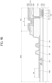
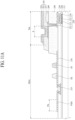
- FIG. 3 is a cross-sectional view briefly illustrating one side of a display panel in FIG. 1 .
- the display panel 110 may include a first substrate 111, a second substrate 112, a thin film transistor layer 10 arranged between the first and second substrates 111 and 112, an organic light emitting diode layer 20, an encapsulation layer 30, and a touch sensing layer 40.
- the first substrate 111 may be a plastic film or a glass substrate.
- the thin film transistor layer 10 is formed on the first substrate 111.
- the thin film transistor layer 10 may include scan lines, data lines, and thin film transistors.
- Each of the thin film transistors includes a gate electrode, a semiconductor layer, source and drain electrodes.
- the scan driver may be formed together with the thin film transistor layer 10.
- the organic light emitting diode layer 20 is formed on the thin film transistor 10.
- the organic light emitting diode layer 20 includes first electrodes, an organic light emitting layer, a second electrode, and banks.
- Each of the organic light emitting layers may include a hole transporting layer, an organic light emitting layer, and an electron transporting layer.
- pixels P are arranged on the area where the organic light emitting diode layer 20 is arranged, the area where the organic light emitting diode layer 20 is arranged may be defined as the display area.
- An area in the periphery of the display area may be defined as the non-display area.
- the encapsulation layer 30 is formed on the organic light emitting diode layer 20.
- the encapsulation layer 30 serves to prevent oxygen and water from being permeated into the organic light emitting diode layer 20.
- the encapsulation layer 30 includes at least one inorganic film.
- the touch sensing layer 40 is formed on the encapsulation layer 30.
- the touch sensing layer 40 includes first and the second touch electrodes for sensing a touch of a user, and may include bridge electrodes for electrically connecting the first touch electrodes or the second touch electrodes.
- FIG. 4 is a plane view briefly illustrating a first substrate according to one example of the present disclosure
- FIG. 5 is a plane view illustrating a touch sensing layer arranged on the first substrate
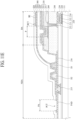
- FIG. 6 is a cross-sectional view illustrating a display device according to the first example of the present disclosure, illustrating a first example taken along line I-I' of FIG. 5 .
- the first substrate 111 is categorized into a display area DA and a non-display area NDA, wherein pixels P are arranged on the display area DA.
- the non-display area NDA surrounds the display area DA, and is provided with a pad area PA where pad electrodes PAD are formed. Also, a dam DAM is formed on the non-display area NDA.
- the thin film transistor layer 10 and the organic light emitting diode layer 20 are formed on the first substrate 111.
- the thin film transistor layer 10 includes thin film transistors 210, a gate insulating film 220, an inter-layer dielectric film 230, and a planarization film 240.
- a buffer film may be arranged on one surface of the first substrate 111.
- the buffer film may be formed on one surface of the first substrate 111 to protect the thin film transistors 210 and light emitting diodes 260 from water permeated through the first substrate 111 which is vulnerable to moisture permeability.
- One surface of the first substrate 111 may be a surface facing the second substrate 112.
- the buffer film may be made of a plurality of inorganic films which are deposited alternately.
- the buffer film may be formed of a multi-layered film of one or more inorganic films of a silicon oxide film (SiOx), a silicon nitride film (SiNx) and SiON, which are deposited alternately.
- the buffer film may be omitted.
- the thin film transistor 210 is arranged on the buffer film.
- the thin film transistor 210 includes an active layer 211, a gate electrode 212, a source electrode 213, and a drain electrode 214.
- the thin film transistor 210 is formed in a top gate mode in which the gate electrode 212 is arranged above the active layer 211 as shown in FIG. 6 , it is to be understood that the thin film transistor of the present disclosure is not limited to the top gate mode. That is, the thin film transistor 210 may be formed in a bottom gate mode in which the gate electrode 212 is arranged below the active layer 211 or a double gate mode in which the gate electrode 212 is arranged above and below the active layer 211.
- the active layer 211 is arranged on the first substrate 111.
- the active layer 211 may be formed of a silicon-based semiconductor material or an oxide-based semiconductor material.
- a light-shielding layer for shielding external light entering the active layer 211 may be formed between the first substrate 111 and the active layer 211.
- the gate insulating film 220 may be arranged on the active layer 211.
- the gate insulating film 220 may be formed of an inorganic film, for example, a silicon oxide film (SiOx), a silicon nitride film (SiNx) or a multi-layered film of the silicon oxide film and the silicon nitride film.
- the gate electrode 212 and the gate line 215 may be arranged on the gate insulating film 220.
- the gate electrode 212 and the gate line 215 may be formed of a single layer or multi-layer comprised of any one of Mo, Al, Cr, Au, Ti, Ni, Nd and Cu or their alloy.
- the inter-layer dielectric film 230 may be arranged on the gate electrode 212 and the gate line 215.
- the inter-layer dielectric film 230 may be formed of an inorganic film, for example, a silicon oxide film (SiOx), a silicon nitride film (SiNx), or a multi-layered film of the silicon oxide film and the silicon nitride film.
- the source electrode 213, the drain electrode 214 the source-drain line 216 and the pad electrode PAD may be arranged on the inter-layer dielectric film 230.
- Each of the source electrode 213 and the drain electrode 214 may be connected to the active layer 211 through a contact hole that passes through the gate insulating film 220 and the inter-layer dielectric film 230.
- the source-drain line 216 and the pad electrode PAD may be connected to the gate line 215 through a contact hole that passes through the inter-layer dielectric film 230.
- the source electrode 213, the drain electrode 214, the source-drain line 216 and the pad electrode PAD may be formed of a single layer or multi-layer comprised of any one of Mo, Al, Cr, Au, Ti, Ni, Nd and Cu or their alloy.
- a passivation film may be formed on the source electrode 213 and the drain electrode 214 to insulate the thin film transistor 210.
- the passivation film may be formed of an inorganic film, for example, a silicon oxide film (SiOx), a silicon nitride film (SiNx), or a multi-layered film of the silicon oxide film and the silicon nitride film.
- the planarization film 240 for planarizing a step difference due to the thin film transistor 210 may be arranged on the source electrode 213 and the drain electrode 214.
- the planarization film 240 may be formed of an organic film such as acrylic resin, epoxy resin, phenolic resin, polyamide resin, and polyimide resin.
- the organic light emitting diode layer 20 is arranged on the thin film transistor layer 10.
- the organic light emitting diode layer 20 includes an organic light emitting diode 250 and a bank 260.
- the organic light emitting diode 250 and the bank 260 are arranged on the planarization film 240.
- the organic light emitting diode 250 includes the first electrode 251, the organic light emitting layer 252, and the second electrode 253.
- the first electrode 251 may be an anode electrode
- the second electrode 253 may be a cathode electrode.
- the first electrode 251 may be formed on the planarization film 240.
- the first electrode 251 may be connected to the source electrode 213 of the thin film transistor 210 through a contact hole that passes through the passivation film and the planarization film 240.
- the first electrode 251 may be formed of conductive material with high reflexibility such as a deposition structure (Ti/Al/Ti) of Al and Ti, a deposition structure (ITO/Al/ITO) of Al and ITO, an APC alloy, or a deposition structure (ITO/APC/ITO) of APC alloy and ITO.
- the APC alloy is an alloy of Ag, Pd and Cu.
- the bank 260 may be arranged on the planarization film 240 to cover an edge of the first electrode 251. That is, the bank 260 serves as a pixel defining film for defining pixels P.
- the bank 260 may be formed of an organic film such as acrylic resin, epoxy resin, phenolic resin, polyamide resin, and polyimide resin.
- the organic light emitting layer 252 is arranged on the first electrode 251 and the bank 260.
- the organic light emitting layer 252 may include a hole transporting layer, at least one light emitting layer, and an electron transporting layer. In this case, when a voltage is applied to the first electrode 251 and the second electrode 253, holes and electrons are moved to the light emitting layer through the hole transporting layer and the electron transporting layer, respectively, and are combined in the organic light emitting layer to emit light.
- the organic light emitting layer 252 may be formed of a white light emitting layer for emitting white light.
- the organic light emitting layer 252 may be arranged to cover the first electrode 251 and the bank 260.
- a color filter (not shown) may be formed on the second substrate 112.
- the organic light emitting layer 252 may be formed of a red light emitting layer for emitting red light, a green light emitting layer for emitting green light, and a blue light emitting layer for emitting blue light.
- the organic light emitting layer 252 may be arranged on the area corresponding to the first electrode 251 and a color filter may not be arranged on the second substrate 112.
- the second electrode 253 is arranged on the organic light emitting layer 252.
- the second electrode 253 may be formed of a transparent conductive material (TCO) such as ITO and IZO, which may transmit light, or a semi-transmissive conductive material such as Mg, Ag, and alloy of Mg and Ag.
- TCO transparent conductive material
- IZO a transparent conductive material
- Mg, Ag, and alloy of Mg and Ag a capping layer may be arranged on the second electrode 253.
- the encapsulation layer 20 is formed not only on the display area DA but also on the non-display area NDA.
- the encapsulation layer 30 includes a dam DAM and an encapsulation film 300.
- the dam DAM is arranged on the non-display area NDA and blocks a flow of an organic film 320 constituting the encapsulation film 300.
- the dam DAM is arranged to surround the outside of the display area DA and blocks a flow of the organic film 320 constituting the encapsulation film 300.
- the dam DAM may also be arranged on the non-display area NDA to block the flow of the organic film 320, thereby allowing the organic film 320 constituting the encapsulation film 300 not to be permeated into the pad electrode PAD exposed by a pad contact hole PCT. Therefore, the dam DAM may prevent the organic film 320 from being exposed to the outside of the display device or from being permeated into the pad electrode PAD.
- Such a dam DAM may include a first dam D1 and a second dam D2.
- the first dam D1 may be arranged to surround the outside of the display area DA to primarily block the flow of the organic film 320 constituting the encapsulation film 300. Also, the first dam D1 may be arranged between the display area DA and the pad area PA to primarily block the flow of the organic film 320 by preventing the organic film 320 from being permeated into the exposed pad electrode PAD.
- the second dam D2 is arranged to surround the outside of the first dam D1, and is spaced apart from the first dam D1 and arranged in parallel with the first dam D1.
- the second dam D2 may secondarily block the flow of the organic film 320 toward the outside of the first dam D1. Therefore, the first dam D1 and the second dam D2 may more effectively prevent the organic film 320 from being exposed to the outside of the display device or from being permeated into the exposed pad electrode PAD.
- Such a dam DAM may be formed simultaneously with the planarization film 240 or the bank 260 and formed of the same material as that of the planarization film 240 or the bank 260.
- the dam DAM may be formed of an organic film such as acrylic resin, epoxy resin, phenolic resin, polyamide resin, and polyimide resin.
- the encapsulation film 300 serves to prevent oxygen or water from being permeated into the organic light emitting layer 252 and the second electrode 253.
- the encapsulation film 300 may include at least one inorganic film and at least one organic film.
- the encapsulation film 300 may include a first inorganic film 310, the organic film 320, and a second inorganic film 330.
- the first inorganic film 310 is arranged on the second electrode 253.
- the first inorganic film 310 is arranged to cover the second electrode 253.
- the first inorganic film 310 according to the first example of the present disclosure covers the second electrode 253 and is extended to the non-display area NDA to cover the dam DAM.
- the first inorganic film 310 according to the first example of the present disclosure is extended to the pad area PA arranged outside the dam DAM but exposes the pad electrode PAD without fully covering the pad electrode PAD.
- the first inorganic film 310 according to the first example of the present disclosure surrounds (e.g. at least partially covers) the pad electrode PAD, and more specifically is arranged to cover the region of the pad electrode PAD outside of the pad contact hole PCT for exposing the pad electrode PAD.
- the first inorganic film 310 is extended to the pad area PA, it is not required to arrange a mask for covering the pad electrode PAD on the pad electrode PAD so as not to form the first inorganic film 310 on the pad area PA. Therefore, in the display device 100 according to the first example of the present disclosure, a mask is not arranged on the pad electrode PAD to prevent arcing from being generated between a boundary surface of the mask and the pad electrode and prevent a defect from being generated due to a high current from the mask, which flows into the display device along the pad electrode PAD.
- the first inorganic film 310 is entirely formed to cover the pad electrode PAD, and the organic film 320 and the second inorganic film 330 are formed and then the pad contact hole PCT is formed by an etching process using a photoresist.
- the organic film 320 is arranged on the first inorganic film 310.
- the organic film 320 may be formed with a suitable thickness to prevent particles from being permeated into the organic light emitting layer 252 and the second electrode 253 by passing through the first inorganic film 310.
- the organic film 320 may be hardened by a hardening process after being deposited in a liquid type through an inkjet process.
- the second inorganic film 330 is arranged on the organic film 320.
- the second inorganic film 330 is arranged to cover the organic film 320.
- the second inorganic film 330 according to the first example of the present disclosure covers the organic film 320 and may be extended to the non-display area NDA to cover the dam DAM.
- the second inorganic film 330 according to the first example of the present disclosure is not formed on the pad area PA. That is, the first inorganic film 310 and the second inorganic film 330 according to the first example of the present disclosure are formed to have their respective ends located to be different from each other.
- a mask may be arranged over the pad electrode PAD.
- the first inorganic film 310 since the first inorganic film 310 is formed on the pad electrode PAD, arcing is not generated between the boundary surface of the mask and the pad electrode PAD even though the mask is arranged over the pad electrode PAD. That is, the first inorganic film 310 serves as an insulating film between the mask and the pad electrode PAD.
- the first inorganic film 310 formed to reach the pad area PA serves as an insulating film, arcing is not generated between the boundary surface of the mask and the pad electrode PAD even though the mask is arranged over the pad electrode PAD during a manufacturing process of the second inorganic film 330.
- Each of the first and second inorganic films 310 and 330 may be formed of a silicon nitride, an aluminum nitride, a zirconium nitride, a titanium nitride, a hafnium nitride, a tantalum nitride, a silicon oxide, an aluminum oxide, or a titanium oxide.
- the organic film 320 may be formed of acrylic resin, epoxy resin, phenolic resin, polyamide resin, or polyimide resin.
- the touch sensing layer 40 is formed on the encapsulation layer 30.
- the touch sensing layer 40 includes a buffer layer 410, bridge electrodes BE, an insulating film 420, first touch electrodes TE1, second touch electrodes TE2, and a passivation film 430.
- the buffer layer 410 is formed on the encapsulation layer 30.
- the buffer layer 410 is formed to cover the encapsulation film 300.
- the buffer layer 410 according to the first example of the present disclosure covers the encapsulation film 300, and is extended to the non-display area NDA to cover the dam DAM.
- the buffer layer 410 according to the first example of the present disclosure is extended to the pad area PA arranged outside the dam DAM but exposes the pad electrode PAD without covering the pad electrode PAD.
- the buffer layer 410 according to the first example of the present disclosure surrounds the pad electrode PAD, and more specifically is arranged to surround the outside of the pad contact hole PCT for exposing the pad electrode PAD.
- the pad electrode PAD may be prevented from being damaged when the bridge electrode BE is formed on the buffer layer 410.
- the bridge electrode BE is formed on the buffer layer 410, and in this case, if the pad electrode PAD is exposed, the pad electrode PAD may be damaged.
- the buffer layer 410 is formed to be extended to the pad area PA, and the bridge electrode BE is formed, whereby the pad electrode PAD may be prevented from being damaged.
- the bridge electrode BE is formed on the buffer layer 410. In order to prevent the first touch electrodes TE1 and the second touch electrodes TE2 from short-circuiting at their crossing areas, the bridge electrode BE electrically connects the first touch electrodes TE1 adjacent to each other in a first direction.
- the bridge electrode BE is formed on a different layer from the first and second touch electrodes TE1 and TE2, and may be connected to the first touch electrodes TE1 adjacent to each other through bridge contact holes BCT.
- the bridge electrode BE may cross the second touch electrode TE2.
- the insulating film 420 is arranged on the bridge electrode BE.
- the insulating film 420 is arranged to cover the bridge electrode BE, thereby insulating the bridge electrode BE from the first and second touch electrodes TE1 and TE2.
- the insulating film 420 according to the first example of the present disclosure covers the bridge electrode BE, and is extended to the non-display area NDA, whereby the insulating film may be formed to reach the pad area PA.
- the insulating film 420 according to the first example of the present disclosure is extended to the pad area PA arranged outside the dam DAM but exposes the pad electrode PAD without covering the pad electrode PAD.
- the insulating film 420 according to the first example of the present disclosure surrounds the pad electrode PAD, and more specifically is arranged to surround the outside of the pad contact hole PCT for exposing the pad electrode PAD.
- the insulating film 420 is extended to the pad area PA, it is not required to arrange a mask for covering the pad electrode PAD on the pad electrode PAD so as not to form the insulating film 420 on the pad area PA.
- the buffer layer 410 and the insulating film 420 formed on the pad electrode PAD may be removed simultaneously to expose the pad electrode PAD during the process of forming the bridge contact hole BCT. That is, the bridge contact hole BCT and the pad contact hole PCT may be formed at the same time.
- the first touch electrodes TE1 and the second touch electrodes TE2 are arranged on the insulating film 420.
- the first touch electrodes TE1, the second touch electrodes TE2, the first touch lines TL1 and the second touch lines TL may be arranged on the same layer.
- the first touch electrodes TE1 are arranged in a first direction (y-axis direction) and connected to each other, and the second touch electrodes TE2 are arranged in a second direction (x-axis direction) and connected to each other.
- the first direction (y-axis direction) may be parallel with the scan lines S1 to Sn
- the second direction (x-axis direction) may be parallel with the data lines D1 to Dm.
- the first direction (y-axis direction) may be parallel with the data lines D1 to Dm
- the second direction (x-axis direction) may be parallel with the scan lines S1 to Sn.
- Each of the first touch electrodes TE1 connected in the first direction (y-axis direction) is electrically insulated from the first touch electrodes TE1 adjacent thereto in the second direction (x-axis direction).
- Each of the second touch electrodes TE2 connected in the second direction (x-axis direction) is electrically insulated from the second touch electrodes TE2 adjacent thereto in the first direction (y-axis direction).
- mutual capacitance corresponding to the touch sensor may be formed on the crossed area of the first touch electrode TE1 and the second touch electrode TE2.
- the first touch electrode TE arranged at one end may be connected to the first touch line TL1 on the non-display area NDA.
- the first touch line TL1 may be extended from the first touch electrode TE1 and then patterned to reach the pad area PA.
- the first touch line TL1 may be connected to the pad electrode PAD in the pad area PA and then connected to the first touch driver 181 through the pad electrode PAD. Therefore, the first touch electrodes TE1 connected with each other in the first direction (y-axis direction) may receive a driving pulse from the first touch driver 181 through the first touch line TL1.
- the second touch electrode TE2 arranged at one end may be connected to the second touch line TL2 on the non-display area NDA.
- the second touch line TL2 may be extended from the second touch electrode TE2 and then patterned to reach the pad area PA.
- the second touch line TL2 may be connected to the pad electrode PAD on the pad area PA and then connected to the second touch driver 182 through the pad electrode PAD. Therefore, the second touch driver 182 may receive amount of charge changes in the touch sensors of the second touch electrodes TE2 connected with each other in the second direction (x-axis direction).
- the passivation film 430 is formed on the first touch electrodes TE1 and the second touch electrodes TE2.
- the passivation film 430 maintains characteristic stabilization of the display device by blocking a harmful environment from the outside.
- the passivation film 430 may be formed not only on the first touch electrodes TE1 and the second touch electrodes TE2 but also between the first touch electrodes TE1 and the second touch electrodes TE2.
- Each of the first touch electrodes TE1 may be insulated from each of the second touch electrodes TE2 by the passivation film 430.
- the touch sensing layer is directly formed on the encapsulation layer 30, it is not required to align the first substrate 111 and the second substrate 112 when the first substrate 111 and the second substrate 112 are bonded to each other.
- the first inorganic film 310 is extended to the pad area PA, it is not required to arrange a mask for covering the pad electrode PAD on the pad electrode PAD so as not to form the first inorganic film 310 on the pad area PA.
- a mask is not arranged on the pad electrode PAD to prevent arcing from being generated between a boundary surface of the mask and the pad electrode and prevent a defect from being generated due to a high current from the mask, which flows into the display device 100 along the pad electrode PAD.
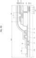
- FIG. 7 is a cross-sectional view illustrating a display device according to the second example of the present disclosure, illustrating a second example taken along line I-I' of FIG. 5 .
- the display device 100 shown in FIG. 7 is the same as the display device 100 according to the first example described in FIG. 6 except a manufacturing method of a pad contact hole PCT according to omission of a buffer layer. Therefore, the manufacturing method of the pad contact hole PCT will be described, and a repeated description of the same elements will be omitted.
- the first inorganic film 310 of the display device 100 according to the second example of the present disclosure is arranged on the second electrode 253.
- the first inorganic film 310 is arranged to cover the second electrode 253.
- the first inorganic film 310 according to the second example of the present disclosure covers the second electrode 253 and is extend to the non-display area NDA to cover the dam DAM.
- the first inorganic film 310 according to the second example of the present disclosure is extended to the pad area PA arranged outside the dam DAM but exposes the pad electrode PAD without covering the pad electrode PAD.
- the first inorganic film 310 according to the second example of the present disclosure surrounds (e.g. at least partially covers) the pad electrode PAD, and more specifically is arranged to surround the outside of the pad contact hole PCT for exposing the pad electrode PAD.
- the first inorganic film 310 is extended to the pad area PA, it is not required to arrange a mask for covering the pad electrode PAD on the pad electrode PAD so as not to form the first inorganic film 310 on the pad area PA. Therefore, in the display device 100 according to the second example of the present disclosure, a mask is not arranged on the pad electrode PAD to prevent arcing from being generated between a boundary surface of the mask and the pad electrode and prevent a defect from being generated due to a high current from the mask, which flows into the display device along the pad electrode PAD.
- the organic film 320 is arranged on the first inorganic film 310, and the second inorganic film 330 is arranged on the organic film 320.
- the second inorganic film 330 is arranged to cover the organic film 320.
- the second inorganic film 330 according to the second example of the present disclosure covers the organic film 320 and may be extended to the non-display area NDA to cover the dam DAM.
- the second inorganic film 330 according to the second example of the present disclosure is not formed on the pad area PA. That is, the first inorganic film 310 and the second inorganic film 330 according to the second example of the present disclosure are formed to have their respective ends located to be different from each other.
- a mask may be arranged over the pad electrode PAD.
- the first inorganic film 310 since the first inorganic film 310 is formed on the pad electrode PAD, arcing is not generated between the boundary surface of the mask and the pad electrode PAD even though the mask is arranged over the pad electrode PAD. That is, the first inorganic film 310 serves as an insulating film between the mask and the pad electrode PAD.
- the first inorganic film 310 formed to reach the pad area PA serves as an insulating film, arcing is not generated between the boundary surface of the mask and the pad electrode PAD even though the mask is arranged over the pad electrode PAD during a manufacturing process of the second inorganic film 330.
- a buffer layer is not formed on the encapsulation film 300, and a bridge electrode BE is formed on the encapsulation film 300.
- the buffer layer is formed on the encapsulation film 300 to protect the pad electrode PAD exposed when the bridge electrode BE is formed in the display device 100 according to the first example of the present disclosure
- the buffer layer is not required in the display device 100 according to the second example of the present disclosure because the pad electrode PAD is not exposed by the first inorganic film 310 when the bridge electrode BE is formed.
- the bridge electrode BE is arranged on the encapsulation film 300, and the insulating film 420 is arranged on the bridge electrode BE.
- the insulating film 420 is arranged to cover the bridge electrode BE, thereby insulating the bridge electrode BE from the first and second touch electrodes TE1 and TE2.
- the insulating film 420 according to the second example of the present disclosure covers the bridge electrode BE, and is extended to the non-display area NDA, whereby the insulating film may be formed to reach the pad area PA.
- the insulating film 420 according to the second example of the present disclosure is extended to the pad area PA arranged outside the dam DAM but exposes the pad electrode PAD without covering the pad electrode PAD.
- the insulating film 420 according to the second example of the present disclosure surrounds the pad electrode PAD, and more specifically is arranged to surround the outside of the pad contact hole PCT for exposing the pad electrode PAD.
- the insulating film 420 is extended to the pad area PA, it is not required to arrange a mask for covering the pad electrode PAD on the pad electrode PAD so as not to form the insulating film 420 on the pad area PA.
- the first inorganic film 310 and the insulating film 420 formed on the pad electrode PAD may be removed simultaneously to expose the pad electrode PAD during the process of forming the bridge contact hole BCT. That is, the bridge contact hole BCT and the pad contact hole PCT may be formed at the same time.
- the first inorganic film 310 is extended to the pad area PA, it is not required to arrange a mask for covering the pad electrode PAD on the pad electrode PAD so as not to form the first inorganic film 310 on the pad area PA.
- a mask is not arranged on the pad electrode PAD to prevent arcing from being generated between a boundary surface of the mask and the pad electrode and prevent a defect from being generated due to a high current from the mask, which flows into the display device 100 along the pad electrode PAD.
- the pad electrode PAD is not exposed by the first inorganic film 310 when the bridge electrode BE is formed, it is not required to form the buffer layer. Therefore, the buffer layer is omitted in the display device 100 according to the second example of the present disclosure, whereby the manufacturing cost may be reduced and the process may be reduced.
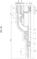
- FIG. 8 is a flow chart illustrating a method of manufacturing a display device according to the first example of the present disclosure
- FIGS. 9a to 9i are cross-sectional views illustrating a method of manufacturing a display device according to the first example of the present disclosure.
- Plane views shown in FIGS. 9a to 9i relate to a method of manufacturing a display device according to the first example of the present disclosure shown in FIG. 6 , and the same reference numerals are given to the same elements as those of FIG. 6 .
- the method of manufacturing a display device according to the first example of the present disclosure will be described with reference to FIG. 8 and FIGS. 9a to 9i .
- pixels P are formed on the display area DA, and a pad electrode PAD and a dam DAM are formed on the non-display area NDA surrounding the display area DA (S801).
- an active layer 211 of a thin film transistor 210 is formed on a first substrate 111.
- an active metal layer is formed on the entire surface of the first substrate 111 by a sputtering method or a MOCVD (Metal Organic Chemical Vapor Deposition) method. Then, the active metal layer is patterned by a mask process using a photoresist pattern to form the active layer 211.
- the active layer 211 may be formed of a silicon based semiconductor material or an oxide based semiconductor material.
- the gate insulating film 220 may be formed of an inorganic film, for example, a silicon oxide film (SiOx), a silicon nitride film (SiNx) or a multi-layered film of the silicon oxide film and the silicon nitride film.
- a gate electrode 212 and a gate line 215 of the thin film transistor 210 are formed on the gate insulating film 220.
- a first metal layer is formed on the entire surface of the gate insulating film 220 by a sputtering method or a MOVCD method.
- the first metal layer is patterned by a mask process using a photoresist pattern to form the gate electrode 212 and the gate line 215.
- the gate electrode 212 and the gate line 212 may be formed of a single layer or multi-layer comprised of any one of Mo, Al, Cr, Au, Ti, Ni, Nd and Cu or their alloy.
- the inter-layer dielectric film 230 may be formed of an inorganic film, for example, a silicon oxide film (SiOx), a silicon nitride film (SiNx), or a multi-layered film of the silicon oxide film and the silicon nitride film.
- contact holes for exposing the active layer 211 by passing through the gate insulating film 220 and the inter-layer dielectric film 230 and contact holes for exposing the gate line 215 by passing through the inter-layer dielectric film 230 are formed.
- source and drain electrodes 213 and 214, a source-drain line 216 and a pad electrode PAD of the thin film transistor 210 are formed on the inter-layer dielectric film 230.
- a second metal layer is formed on the entire surface of on the inter-layer dielectric film 230 by a sputtering method or a MOVCD method.
- the second metal layer is patterned by a mask process using a photoresist pattern to form the source and drain electrodes 213 and 214, the source-drain line 216 and the pad electrode PAD.
- Each of the source and drain electrodes 213 and 214 may be connected to the active layer 211 through contact holes that pass through the gate insulating film 220 and the inter-layer dielectric film 230.
- the source-drain line 216 and the pad electrode PAD may be connected to the gate line 215 through contact holes that pass through the inter-layer dielectric film 230.
- Each of the source and drain electrodes 213 and 214, the source-drain line 216 and the pad electrode PAD may be formed of a single layer or multi-layer comprised of any one of Mo, Al, Cr, Au, Ti, Ni, Nd and Cu or their alloy.
- planarization film 240 for planarizing a step difference due to the thin film transistor 210 is formed on the source and drain electrodes 213 and 214 of the thin film transistor 210.
- the planarization film 240 may be formed of an organic film such as acrylic resin, epoxy resin, phenolic resin, polyamide resin, and polyimide resin.
- an organic light emitting diode 250 is formed on the planarization film 240.
- a first electrode 251 of the organic light emitting diode 250 is formed on the planarization film 240.
- a third metal layer is formed on the entire surface of the planarization film 240 using a sputtering method or a MOVCD method. Then, the third metal layer is patterned by a mask process using a photoresist pattern to form the first electrode 251.
- the first electrode 251 may be connected to the source electrode 213 of the thin film transistor 210 through a contact hole that passes through the planarization film 240.
- the first electrode 251 may be formed of a conductive material with high reflexibility such as a deposition structure (Ti/Al/Ti) of Al and Ti, a deposition structure (ITO/Al/ITO) of Al and ITO, an APC alloy, or a deposition structure (ITO/APC/ITO) of APC alloy and ITO.
- a bank 260 is formed on the planarization film 240 to cover an edge of the first electrode 251, and a dam DAM is also formed together with the bank 260.
- the dam DAM is formed on the non-display area NDA.
- Each of the dam DAM and the bank 260 may be formed of an organic film such as acrylic resin, epoxy resin, phenolic resin, polyamide resin, and polyimide resin.
- the dam DAM is formed simultaneously with the bank 260 but is not limited to this example.
- the dam DAM may be formed simultaneously with the planarization film 250.
- an organic light emitting layer 252 is formed on the first electrode 251 and the bank 260 by a deposition process or a solution process.
- the second electrode 253 is formed on the organic light emitting layer 252.
- the second electrode 253 may be a common layer that is commonly formed on the pixels P.
- the second electrode 253 may be formed of a transparent conductive material (TCO) such as ITO and IZO, which may transmit light.
- TCO transparent conductive material
- the second electrode 253 may be formed by physics vapor deposition such as a sputtering method.
- a capping layer may be formed on the second electrode 253.
- a first inorganic film 310 is entirely formed on the first substrate 111 (S802).
- the first inorganic film 310 according to the first example of the present disclosure covers the second electrode 253, and is extended to the non-display area NDA to cover the dam DAM and the pad electrode PAD.
- the first inorganic film 310 is extended to the pad area PA, it is not required to arrange a mask for covering the pad electrode PAD on the pad electrode PAD so as not to form the first inorganic film 310 on the pad area PA.
- a mask is not arranged on the pad electrode PAD to prevent arcing from being generated between a boundary surface of the mask and the pad electrode and prevent a defect from being generated due to a high current from the mask, which flows into the display device along the pad electrode PAD.
- an organic film 320 and a second inorganic film 330 are formed on the first inorganic film 310 (S803).
- the organic film 320 is formed to cover the first inorganic film 310.
- the organic film 320 is preferably formed with a sufficient thickness to prevent particles from being permeated into the organic light emitting layer 252 and the second electrode 253 by passing through the first inorganic film 310.
- the second inorganic film 320 is formed to cover the organic film 320.
- the mask for covering the pad electrode PAD is arranged over (but not on) the pad electrode PAD, whereby the second inorganic film 330 is formed except an upper portion of the pad electrode PAD.
- Each of the first and second inorganic films 310 and 330 may be formed of a silicon oxide, a silicon nitride, a silicon oxynitride, an aluminum oxide, an aluminum nitride, a zirconium nitride, a titanium nitride, a hafnium nitride, a tantalum nitride, or a titanium oxide.
- the organic film 320 may be formed of acrylic resin, epoxy resin, phenolic resin, polyamide resin, or polyimide resin.
- a photoresist (PR) pattern is formed on the first substrate 111 except the pad area PA (S804).
- the first inorganic film 301 formed on the pad electrode PAD is removed (S805).
- a dry etching process is performed on the first substrate 111 on which the photoresist pattern is formed.
- the first inorganic film 310 of the pad area PA where the photoresist pattern is not formed is removed by the dry etching process, and the pad electrode PAD is exposed. Then, the photoresist pattern is removed.
- a buffer layer 410 is entirely formed on the first substrate 111 (S806).
- the buffer layer 410 according to the first example of the present disclosure covers the encapsulation film 300, and is extended to the non-display area NDA to cover the dam DAM and the pad electrode PAD.
- the pad electrode PAD may be prevented from being damaged when the bridge electrode BE is formed on the buffer layer 410.
- the bridge electrode BE is formed on the buffer layer 410, and in this case, if the pad electrode PAD is exposed, the pad electrode PAD may be damaged.
- the buffer layer 410 is formed to be extended to the pad area PA, and the bridge electrode BE is formed, whereby the pad electrode PAD may be prevented from being damaged.
- the bridge electrode BE is formed on the buffer layer 410, and the insulating film 420 is entirely formed on the first substrate 111 (S807).
- a fourth metal layer is formed on the entire surface of the buffer film 410 by a sputtering method or a MOVCD method. Then, the fourth metal layer is patterned by a mask process using a photoresist pattern to form the bridge electrode BE.
- the insulating film 420 is entirely formed on the first substrate 111.
- the insulating film 420 according to the first example of the present disclosure covers the bridge electrode BE, and is extended to the non-display area NDA to cover the dam DAM and the pad electrode PAD.
- the insulating film 420 is extended to the pad area PA, it is not required to arrange a mask for covering the pad electrode PAD on the pad electrode PAD so as not to form the insulating film 420 on the pad area PA.
- a bridge contact hole BCT for exposing the bridge electrode BE and a pad contact hole PCT for exposing the pad electrode PAD are formed (S808).
- the bridge contact hole BCT for exposing the bridge electrode BE by passing through the insulating film 420 and the pad contact hole PCT for exposing the pad electrode PAD are formed at the same time.
- the buffer layer 410 and the insulating film 420 formed on the pad electrode PAD may be removed simultaneously to expose the pad electrode PAD during the process of forming the bridge contact hole BCT.
- the bridge electrode BE may be connected to first touch electrodes TE1 through the bridge contact hole BCT, which passes through the insulating film 420, to electrically connect the first touch electrodes TE1.
- the first touch electrode TE1 a second touch electrode TE2 and touch lines TL1 and TL2 are formed, the first touch electrode E1 is electrically connected with the bridge electrode BE and the pad electrode PAD, and a passivation film 430 is formed (S809).
- first touch electrodes TE1, the second touch electrodes TE2 and the touch lines TL1 and TL2 are formed on the buffer layer 410.
- the first touch electrodes TE1 are arranged in a first direction to be spaced apart from each other at a constant space, and the second touch electrodes TE2 are arranged in a second direction to be connected to each other.
- each of the first touch electrodes TE1 and the second touch electrodes TE2 may have shapes of a rectangle, an octagon, a circle, or a rhombus.
- the first touch electrode TE1 arranged at one end may be connected to the first touch line TL1 on the non-display area NDA.
- the first touch line TL1 may be extended from the first touch electrode TE1 and then patterned to reach the pad area PA.
- the first touch electrode TE1 and the first touch line TL1 may be formed on the same layer, and may be formed of the same material.
- the second touch electrode TE2 arranged at one end may be connected to the second touch line TL2 on the non-display area NDA.
- the second touch line TL2 may be extended from the second touch electrode TE2 and then patterned to reach the pad area PA.
- the second touch electrode TE2 and the second touch line TL2 may be formed on the same layer, and may be formed of the same material.
- the first touch electrodes TE1, the second touch electrodes TE2, the first touch lines TL1, and the second touch lines TL2 may be formed of a transparent conductive material (TCO) such as ITO and IZO, which may transmit light.
- TCO transparent conductive material
- a fifth metal layer is formed on the entire surface of the insulating film 420 by a sputtering method or a MOVCD method. Then, the fifth metal layer is patterned by a mask process using a photoresist pattern to form the first touch electrodes TE1, the second touch electrodes TE2, the first touch lines TL1, and the second touch lines TL2.
- a passivation film 430 is formed on the first touch electrode TE1 and the second touch electrode TE2.
- the first substrate 111 where the passivation film 430 is formed is bonded to the second substrate 112.
- the first substrate 111 and the second substrate 112 may be bonded to each other in such a manner that the passivation film 430 of the first substrate 111 and the second substrate 112 are adhered to each other using an adhesive layer (not shown).
- the adhesive layer (not shown) may be an optically clear resin (OCR) or an optically clear adhesive film (OCA).
- the first inorganic film 310 is extended to the pad area PA, it is not required to arrange a mask for covering the pad electrode PAD on the pad electrode PAD so as not to form the first inorganic film 310 on the pad area PA. Therefore, in the display device 100 according to the first example of the present disclosure, a mask is not arranged on the pad electrode PAD to prevent arcing from being generated between a boundary surface of the mask and the pad electrode and prevent a defect from being generated due to a high current from the mask, which flows into the display device along the pad electrode PAD.
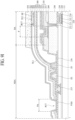
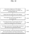
- FIG. 10 is a flow chart illustrating a method of manufacturing a display device according to the second example of the present disclosure
- FIGS. 11a to 11f are cross-sectional views illustrating a method of manufacturing a display device according to the second example of the present disclosure.
- Plane views shown in FIGS. 11a to 11f relate to a method of manufacturing a display device according to the second example of the present disclosure shown in FIG. 7 , and the same reference numerals are given to the same elements as those of FIG. 7 .
- the method of manufacturing a display device according to the second example of the present disclosure will be described with reference to FIG. 10 and FIGS. 11a to 11f .
- pixels P are formed on the display area DA, and a pad electrode PAD and a dam DAM are formed on the non-display area NDA surrounding the display area DA (S1101).
- a first inorganic film 310 is entirely formed on the first substrate 111 (S1102).
- an organic film 320 and a second inorganic film 330 are formed on the first inorganic film 310 (S1 103).
- the method of manufacturing a display device 100 which is shown in FIGS. 11a to 11c , is the same as the method of manufacturing a display device 100 according to the first example described with reference to FIGS. 9a to 9c . Therefore, repeated description of the same elements will be omitted.
- the bridge electrode BE is formed on the buffer layer 410, and the insulating film 420 is entirely formed on the first substrate 111 (S1004).
- the buffer layer is not formed on the encapsulation film 300, and the bridge electrode BE is formed on the encapsulation film 300.
- the buffer layer is formed on the encapsulation film 300 to protect the pad electrode PAD exposed when the bridge electrode BE is formed in the display device 100 according to the first example of the present disclosure
- the buffer layer is not required in the display device 100 according to the second example of the present disclosure because the pad electrode PAD is not exposed by the first inorganic film 310 when the bridge electrode BE is formed. Therefore, the buffer layer is omitted in the display device 100 according to the second example of the present disclosure, whereby the manufacturing cost may be reduced and the process may be reduced.
- a fourth metal layer is formed on the entire surface of the second inorganic film 330 by a sputtering method or a MOVCD method. Then, the fourth metal layer is patterned by a mask process using a photoresist pattern to form the bridge electrode BE.
- the insulating film 420 is entirely formed on the first substrate 111.
- the insulating film 420 according to the second example of the present disclosure covers the bridge electrode BE, and is extended to the non-display area NDA to cover the dam DAM and the pad electrode PAD.
- the insulating film 420 is extended to the pad area PA, it is not required to arrange a mask for covering the pad electrode PAD on the pad electrode PAD so as not to form the insulating film 420 on the pad area PA.
- a bridge contact hole BCT for exposing the bridge electrode BE and a pad contact hole PCT for exposing the pad electrode PAD are formed (S1005).
- the bridge contact hole BCT for exposing the bridge electrode BE by passing through the insulating film 420 and the pad contact hole PCT for exposing the pad electrode PAD by passing through the insulating film 420 are formed at the same time.
- the bridge electrode BE may be connected to first touch electrodes TE1 through the bridge contact hole BCT, which passes through the insulating film 420, to electrically connect the first touch electrodes TE1.
- the first touch electrode TE1 a second touch electrode TE2 and touch lines TL1 and TL2 are formed, the first touch electrode E1 is electrically connected with the bridge electrode BE and the pad electrode PAD, and a passivation film 430 is formed (S1006).
- the method of manufacturing a display device 100 which is shown in FIGS. 11e , is the same as the method of manufacturing a display device 100 according to the first example described with reference to FIG. 9i . Therefore, repeated description of the same elements will be omitted.
- the first inorganic film 310 is formed to be extended to the pad area PA, it is not required to arrange a mask for covering the pad electrode PAD on the pad electrode PAD so as not to form the first inorganic film 310 on the pad area PA.
- a mask is not arranged on the pad electrode PAD to prevent arcing from being generated between a boundary surface of the mask and the pad electrode and prevent a defect from being generated due to a high current from the mask, which flows into the display device along the pad electrode PAD.
- the pad electrode PAD is not exposed by the first inorganic film 310 when the bridge electrode BE is formed, it is not required to form the buffer layer. Therefore, the buffer layer is omitted in the display device 100 according to the second example of the present disclosure, whereby the manufacturing cost may be reduced and the process may be reduced.
- the first inorganic film is formed to be extended to the pad area PA, it is not required to arrange a mask for covering the pad electrode on the pad electrode so as not to form the first inorganic film on the pad area PA.
- a mask is not arranged on the pad electrode to prevent arcing from being generated between a boundary surface of the mask and the pad electrode and prevent a defect from being generated due to a high current from the mask, which flows into the display device along the pad electrode.
- the manufacturing cost may be reduced and the process may be reduced.
- the disclosure comprises the following items:
Landscapes
- Engineering & Computer Science (AREA)
- Theoretical Computer Science (AREA)
- General Engineering & Computer Science (AREA)
- Physics & Mathematics (AREA)
- General Physics & Mathematics (AREA)
- Human Computer Interaction (AREA)
- Microelectronics & Electronic Packaging (AREA)
- Inorganic Chemistry (AREA)
- Chemical & Material Sciences (AREA)
- Optics & Photonics (AREA)
- Computer Networks & Wireless Communication (AREA)
- Electroluminescent Light Sources (AREA)
- Devices For Indicating Variable Information By Combining Individual Elements (AREA)
- Liquid Crystal (AREA)
Applications Claiming Priority (2)
| Application Number | Priority Date | Filing Date | Title |
|---|---|---|---|
| KR1020170143995A KR102408164B1 (ko) | 2017-10-31 | 2017-10-31 | 표시 장치 및 그의 제조방법 |
| EP18203826.5A EP3477726B1 (de) | 2017-10-31 | 2018-10-31 | Anzeigevorrichtung |
Related Parent Applications (2)
| Application Number | Title | Priority Date | Filing Date |
|---|---|---|---|
| EP18203826.5A Division EP3477726B1 (de) | 2017-10-31 | 2018-10-31 | Anzeigevorrichtung |
| EP18203826.5A Division-Into EP3477726B1 (de) | 2017-10-31 | 2018-10-31 | Anzeigevorrichtung |
Publications (2)
| Publication Number | Publication Date |
|---|---|
| EP4236653A2 true EP4236653A2 (de) | 2023-08-30 |
| EP4236653A3 EP4236653A3 (de) | 2023-10-11 |
Family
ID=64048987
Family Applications (2)
| Application Number | Title | Priority Date | Filing Date |
|---|---|---|---|
| EP23178795.3A Pending EP4236653A3 (de) | 2017-10-31 | 2018-10-31 | Anzeigevorrichtung |
| EP18203826.5A Active EP3477726B1 (de) | 2017-10-31 | 2018-10-31 | Anzeigevorrichtung |
Family Applications After (1)
| Application Number | Title | Priority Date | Filing Date |
|---|---|---|---|
| EP18203826.5A Active EP3477726B1 (de) | 2017-10-31 | 2018-10-31 | Anzeigevorrichtung |
Country Status (5)
| Country | Link |
|---|---|
| US (3) | US10971571B2 (de) |
| EP (2) | EP4236653A3 (de) |
| JP (2) | JP6925310B2 (de) |
| KR (2) | KR102408164B1 (de) |
| CN (2) | CN109728040B (de) |
Families Citing this family (52)
| Publication number | Priority date | Publication date | Assignee | Title |
|---|---|---|---|---|
| KR101974086B1 (ko) * | 2016-09-30 | 2019-05-02 | 삼성디스플레이 주식회사 | 표시모듈 |
| KR102325262B1 (ko) * | 2017-06-01 | 2021-11-10 | 엘지디스플레이 주식회사 | 터치 디스플레이 장치, 터치 디스플레이 패널 및 터치 디스플레이 패널의 제조 방법 |
| KR102408164B1 (ko) * | 2017-10-31 | 2022-06-10 | 엘지디스플레이 주식회사 | 표시 장치 및 그의 제조방법 |
| US11508799B2 (en) * | 2018-03-28 | 2022-11-22 | Sharp Kabushiki Kaisha | Display device comprising frame region surrounding display region |
| JP7150527B2 (ja) * | 2018-08-31 | 2022-10-11 | 株式会社ジャパンディスプレイ | 表示装置及び表示装置の製造方法 |
| KR20200028567A (ko) * | 2018-09-06 | 2020-03-17 | 삼성디스플레이 주식회사 | 표시 장치 |
| KR102563782B1 (ko) * | 2018-10-19 | 2023-08-04 | 엘지디스플레이 주식회사 | 표시 장치 |
| KR102661283B1 (ko) * | 2018-11-26 | 2024-05-02 | 삼성디스플레이 주식회사 | 표시 기판, 이의 제조 방법, 및 이를 포함하는 표시 장치 |
| CN110096174A (zh) * | 2019-04-18 | 2019-08-06 | 武汉华星光电半导体显示技术有限公司 | 柔性触控屏结构及其制作方法 |
| KR102941498B1 (ko) * | 2019-04-22 | 2026-03-19 | 삼성디스플레이 주식회사 | 디스플레이 장치 |
| CN110071228A (zh) * | 2019-04-30 | 2019-07-30 | 武汉华星光电半导体显示技术有限公司 | 一种显示面板 |
| KR102675479B1 (ko) * | 2019-06-14 | 2024-06-13 | 삼성디스플레이 주식회사 | 표시 장치 및 표시 장치의 제조 방법 |
| KR102843099B1 (ko) | 2019-07-12 | 2025-08-06 | 삼성디스플레이 주식회사 | 표시 장치 및 표시 장치의 제조 방법 |
| KR102813429B1 (ko) * | 2019-07-19 | 2025-05-27 | 엘지디스플레이 주식회사 | 유기발광 표시장치 |
| KR102754154B1 (ko) * | 2019-08-05 | 2025-01-10 | 엘지디스플레이 주식회사 | 표시 장치 |
| KR102840643B1 (ko) * | 2019-08-12 | 2025-07-30 | 엘지디스플레이 주식회사 | 전계 발광 표시 장치 |
| CN110634917A (zh) * | 2019-08-19 | 2019-12-31 | 武汉华星光电半导体显示技术有限公司 | 显示面板、显示装置及显示面板的制作方法 |
| KR20210024360A (ko) | 2019-08-22 | 2021-03-05 | 삼성디스플레이 주식회사 | 표시 장치 및 표시 장치의 제조방법 |
| KR102897994B1 (ko) | 2019-09-16 | 2025-12-10 | 삼성디스플레이 주식회사 | 표시 장치 |
| KR102889931B1 (ko) | 2019-10-02 | 2025-11-25 | 삼성디스플레이 주식회사 | 유기 발광 표시 장치 |
| KR102891041B1 (ko) * | 2019-11-15 | 2025-11-27 | 삼성디스플레이 주식회사 | 표시 장치 |
| CN110808275A (zh) * | 2019-11-15 | 2020-02-18 | 昆山工研院新型平板显示技术中心有限公司 | 显示面板及其制备方法、以及显示装置 |
| KR102880686B1 (ko) * | 2019-12-04 | 2025-11-06 | 삼성디스플레이 주식회사 | 전자 장치 |
| KR102950450B1 (ko) | 2019-12-03 | 2026-04-09 | 엘지디스플레이 주식회사 | 디스플레이 장치 |
| KR102851564B1 (ko) * | 2019-12-10 | 2025-08-28 | 엘지디스플레이 주식회사 | 표시장치 |
| KR102941359B1 (ko) * | 2019-12-24 | 2026-03-18 | 엘지디스플레이 주식회사 | 투명 표시 장치 |
| KR102854144B1 (ko) * | 2019-12-30 | 2025-09-02 | 엘지디스플레이 주식회사 | 투명 표시 장치 |
| KR102735417B1 (ko) * | 2019-12-31 | 2024-11-27 | 엘지디스플레이 주식회사 | 표시장치 |
| KR102899232B1 (ko) * | 2020-02-04 | 2025-12-12 | 삼성디스플레이 주식회사 | 표시 장치 및 그의 제조 방법 |
| KR102909043B1 (ko) | 2020-03-17 | 2026-01-07 | 삼성디스플레이 주식회사 | 디스플레이 장치 |
| EP4135041B1 (de) * | 2020-04-09 | 2025-06-18 | BOE Technology Group Co., Ltd. | Anzeigetafel und anzeigevorrichtung |
| CN113675356A (zh) * | 2020-05-14 | 2021-11-19 | Ncd有限公司 | 在薄膜封装体上形成触摸屏板的方法 |
| KR102892879B1 (ko) * | 2020-06-22 | 2025-11-28 | 삼성디스플레이 주식회사 | 디스플레이 장치 |
| KR102931794B1 (ko) * | 2020-07-21 | 2026-02-25 | 엘지디스플레이 주식회사 | 표시 장치 |
| JP7077468B2 (ja) * | 2020-11-11 | 2022-05-30 | ヤフー株式会社 | 情報処理装置、情報処理方法及び情報処理プログラム |
| KR102846652B1 (ko) * | 2020-11-18 | 2025-08-14 | 엘지디스플레이 주식회사 | 표시장치 |
| KR20220082315A (ko) * | 2020-12-10 | 2022-06-17 | 엘지디스플레이 주식회사 | 터치 스크린 일체형 발광 표시 장치 |
| KR102873653B1 (ko) | 2020-12-11 | 2025-10-17 | 엘지디스플레이 주식회사 | 유기발광 표시장치 |
| US20240237434A9 (en) * | 2021-03-25 | 2024-07-11 | Sharp Display Technology Corporation | Display device |
| KR102941504B1 (ko) * | 2021-11-08 | 2026-03-20 | 삼성디스플레이 주식회사 | 표시 장치 및 이의 제조 방법 |
| KR20230071893A (ko) * | 2021-11-16 | 2023-05-24 | 삼성디스플레이 주식회사 | 표시 장치 및 그 제조 방법 |
| KR20230100496A (ko) | 2021-12-28 | 2023-07-05 | 엘지디스플레이 주식회사 | 터치 디스플레이 장치 |
| KR20230141195A (ko) * | 2022-03-31 | 2023-10-10 | 엘지디스플레이 주식회사 | 발광 표시 장치 |
| CN116960109A (zh) | 2022-04-15 | 2023-10-27 | 睿生光电股份有限公司 | 检测装置及其制造方法 |
| TWI841951B (zh) * | 2022-04-15 | 2024-05-11 | 睿生光電股份有限公司 | 偵測裝置及其製造方法 |
| CN114860110B (zh) * | 2022-05-19 | 2026-01-16 | 武汉华星光电半导体显示技术有限公司 | 触控显示面板及显示装置 |
| JP2024016581A (ja) * | 2022-07-26 | 2024-02-07 | 株式会社ジャパンディスプレイ | 表示装置およびその製造方法 |
| KR20240020765A (ko) * | 2022-08-08 | 2024-02-16 | 삼성디스플레이 주식회사 | 표시 패널 및 이를 포함하는 전자 기기 |
| JP2024037350A (ja) * | 2022-09-07 | 2024-03-19 | 株式会社ジャパンディスプレイ | 表示装置 |
| KR20240106258A (ko) * | 2022-12-29 | 2024-07-08 | 엘지디스플레이 주식회사 | 디스플레이 장치 |
| KR20240118284A (ko) * | 2023-01-27 | 2024-08-05 | 엘지디스플레이 주식회사 | 유기 발광 표시 장치 및 그 제조방법 |
| KR20240120483A (ko) * | 2023-01-31 | 2024-08-07 | 엘지디스플레이 주식회사 | 터치 표시 장치 |
Family Cites Families (52)
| Publication number | Priority date | Publication date | Assignee | Title |
|---|---|---|---|---|
| JP4384293B2 (ja) * | 1999-07-06 | 2009-12-16 | エーユー オプトロニクス コーポレイション | 液晶表示パネル、表示装置、識別マーク検出装置、検出表示システム、tftアレイ・リペア装置及び識別マーク検出方法 |
| JP2003050380A (ja) * | 2001-08-07 | 2003-02-21 | Toshiba Corp | アレイ基板の検査方法 |
| US7109653B2 (en) * | 2002-01-15 | 2006-09-19 | Seiko Epson Corporation | Sealing structure with barrier membrane for electronic element, display device, electronic apparatus, and fabrication method for electronic element |
| JP2005309230A (ja) * | 2004-04-23 | 2005-11-04 | Tohoku Pioneer Corp | 自発光表示モジュールおよび同モジュールを搭載した電子機器、ならびに同モジュールにおける欠陥状態の検証方法 |
| JP2006309028A (ja) * | 2005-04-28 | 2006-11-09 | Sanyo Epson Imaging Devices Corp | 表示装置および表示装置の製造方法 |
| KR20080067158A (ko) * | 2007-01-15 | 2008-07-18 | 삼성전자주식회사 | 표시장치 |
| JP4518123B2 (ja) * | 2007-09-12 | 2010-08-04 | ソニー株式会社 | 表示パネル及びパネル検査装置 |
| KR101496844B1 (ko) * | 2008-07-28 | 2015-02-27 | 삼성디스플레이 주식회사 | 터치 스크린 표시 장치 및 그 구동 방법 |
| WO2010038514A1 (ja) * | 2008-10-02 | 2010-04-08 | シャープ株式会社 | 表示装置用基板、表示装置用基板の製造方法、表示装置、液晶表示装置、液晶表示装置の製造方法及び有機エレクトロルミネセンス表示装置 |
| CN103019420A (zh) | 2011-09-21 | 2013-04-03 | 联胜(中国)科技有限公司 | 触控显示面板 |
| KR101971164B1 (ko) * | 2011-11-08 | 2019-08-14 | 삼성디스플레이 주식회사 | 터치 기판 및 이를 포함하는 표시 장치 |
| KR101453880B1 (ko) | 2012-11-29 | 2014-10-22 | 삼성디스플레이 주식회사 | 유기 발광 표시 장치 및 이의 제조 방법 |
| KR101980766B1 (ko) * | 2012-12-27 | 2019-05-21 | 엘지디스플레이 주식회사 | 터치 패널 내장형 유기 발광 다이오드 표시 장치 |
| US20150255748A1 (en) * | 2014-03-10 | 2015-09-10 | Samsung Sdi Co., Ltd. | Low permeation gas ultra-barrier with wet passivation layer |
| US10032844B2 (en) * | 2014-12-29 | 2018-07-24 | Lg Display Co., Ltd. | Organic light emitting display device and method of manufacturing the same |
| US9287329B1 (en) * | 2014-12-30 | 2016-03-15 | Lg Display Co., Ltd. | Flexible display device with chamfered polarization layer |
| KR102391361B1 (ko) * | 2015-01-14 | 2022-04-27 | 삼성디스플레이 주식회사 | 유기 발광 표시 장치 |
| KR102314470B1 (ko) * | 2015-03-09 | 2021-10-20 | 삼성디스플레이 주식회사 | 유기 발광 표시 장치 |
| KR102362189B1 (ko) * | 2015-04-16 | 2022-02-11 | 삼성디스플레이 주식회사 | 유기 발광 표시 장치 |
| KR20160128513A (ko) * | 2015-04-28 | 2016-11-08 | 삼성디스플레이 주식회사 | 터치 센서를 포함하는 표시 장치 |
| KR102446857B1 (ko) * | 2015-05-26 | 2022-09-23 | 삼성디스플레이 주식회사 | 표시 장치 |
| KR101763616B1 (ko) * | 2015-07-29 | 2017-08-02 | 삼성디스플레이 주식회사 | 유기 발광 표시 장치 |
| KR102401080B1 (ko) | 2015-09-30 | 2022-05-23 | 삼성디스플레이 주식회사 | 표시 장치 |
| KR102512480B1 (ko) * | 2015-11-30 | 2023-03-22 | 엘지디스플레이 주식회사 | 표시장치 |
| KR101765103B1 (ko) * | 2015-12-18 | 2017-08-04 | 엘지디스플레이 주식회사 | 유기 발광 표시 장치 |
| KR102483229B1 (ko) * | 2015-12-31 | 2022-12-29 | 엘지디스플레이 주식회사 | 유기발광 표시장치 |
| KR102531673B1 (ko) * | 2016-04-07 | 2023-05-12 | 삼성디스플레이 주식회사 | 디스플레이 장치 |
| KR102601207B1 (ko) * | 2016-07-29 | 2023-11-13 | 삼성디스플레이 주식회사 | 표시장치 |
| KR101979444B1 (ko) * | 2016-07-29 | 2019-05-17 | 삼성디스플레이 주식회사 | 표시장치 |
| KR101998831B1 (ko) * | 2016-07-29 | 2019-07-11 | 삼성디스플레이 주식회사 | 표시 장치 |
| KR102586113B1 (ko) * | 2016-08-31 | 2023-10-06 | 엘지디스플레이 주식회사 | 터치스크린 내장형 표시패널, 터치스크린 내장형 표시장치, 통합 구동 회로 및 구동 방법 |
| KR102405120B1 (ko) * | 2016-09-29 | 2022-06-08 | 삼성디스플레이 주식회사 | 표시 장치 및 표시 장치의 제조방법 |
| KR102668610B1 (ko) * | 2016-10-21 | 2024-05-24 | 삼성디스플레이 주식회사 | 표시 장치 |
| CN106816456B (zh) * | 2016-12-16 | 2019-12-24 | 上海天马微电子有限公司 | 一种有机发光二极管显示面板及显示器 |
| JP6827332B2 (ja) * | 2017-02-01 | 2021-02-10 | 株式会社ジャパンディスプレイ | 表示装置 |
| CN106775173B (zh) * | 2017-02-07 | 2019-12-20 | 上海天马微电子有限公司 | 一种触控显示面板和触控显示装置 |
| KR102657718B1 (ko) * | 2017-02-09 | 2024-04-16 | 삼성디스플레이 주식회사 | 표시 장치 및 표시 장치의 제조방법 |
| CN106803514B (zh) * | 2017-02-22 | 2020-06-30 | 上海天马微电子有限公司 | 一种集成触控的有机发光二极管显示装置 |
| CN106951125B (zh) | 2017-03-30 | 2019-09-13 | 上海天马微电子有限公司 | 一种触控显示面板及触控显示装置 |
| CN107068720B (zh) * | 2017-04-19 | 2019-08-27 | 上海天马微电子有限公司 | 一种有机发光二极管显示面板及显示装置 |
| JP2018181799A (ja) | 2017-04-21 | 2018-11-15 | 株式会社ジャパンディスプレイ | 表示装置、および表示装置の製造方法 |
| KR102438255B1 (ko) | 2017-05-31 | 2022-08-30 | 엘지디스플레이 주식회사 | 표시 장치 |
| KR102408164B1 (ko) * | 2017-10-31 | 2022-06-10 | 엘지디스플레이 주식회사 | 표시 장치 및 그의 제조방법 |
| KR102493681B1 (ko) * | 2018-03-30 | 2023-01-31 | 엘지디스플레이 주식회사 | 터치 디스플레이 장치 및 터치 센싱 방법 |
| KR102463801B1 (ko) * | 2018-04-03 | 2022-11-03 | 엘지디스플레이 주식회사 | 터치 디스플레이 장치 및 터치 센싱 방법 |
| KR102463812B1 (ko) * | 2018-04-03 | 2022-11-03 | 엘지디스플레이 주식회사 | 터치 디스플레이 장치 및 터치 센싱 방법 |
| KR102461365B1 (ko) * | 2018-04-04 | 2022-10-31 | 엘지디스플레이 주식회사 | 터치 디스플레이 패널 및 터치 디스플레이 장치 |
| KR102498978B1 (ko) * | 2018-05-02 | 2023-02-10 | 엘지디스플레이 주식회사 | 터치 디스플레이장치 |
| KR102553542B1 (ko) * | 2018-07-20 | 2023-07-10 | 엘지디스플레이 주식회사 | 터치 디스플레이 패널, 터치 디스플레이 장치 |
| KR102553544B1 (ko) * | 2018-07-20 | 2023-07-10 | 엘지디스플레이 주식회사 | 터치 디스플레이 장치, 터치 회로 및 구동 방법 |
| KR102553530B1 (ko) * | 2018-07-20 | 2023-07-10 | 엘지디스플레이 주식회사 | 터치 디스플레이 패널, 터치 디스플레이 장치 및 그 구동 방법 |
| KR102671256B1 (ko) * | 2018-11-23 | 2024-06-03 | 엘지디스플레이 주식회사 | 터치 패널 및 터치 디스플레이 장치 |
-
2017
- 2017-10-31 KR KR1020170143995A patent/KR102408164B1/ko active Active
-
2018
- 2018-10-30 JP JP2018204057A patent/JP6925310B2/ja active Active
- 2018-10-31 US US16/176,061 patent/US10971571B2/en active Active
- 2018-10-31 CN CN201811286920.9A patent/CN109728040B/zh active Active
- 2018-10-31 EP EP23178795.3A patent/EP4236653A3/de active Pending
- 2018-10-31 EP EP18203826.5A patent/EP3477726B1/de active Active
- 2018-10-31 CN CN202310504663.6A patent/CN116507167A/zh active Pending
-
2021
- 2021-03-04 US US17/192,043 patent/US11600686B2/en active Active
- 2021-08-03 JP JP2021127271A patent/JP7311562B2/ja active Active
-
2022
- 2022-06-08 KR KR1020220069365A patent/KR102514449B1/ko active Active
-
2023
- 2023-01-24 US US18/100,828 patent/US11882740B2/en active Active
Also Published As
| Publication number | Publication date |
|---|---|
| US10971571B2 (en) | 2021-04-06 |
| KR102514449B1 (ko) | 2023-03-24 |
| US20210193787A1 (en) | 2021-06-24 |
| US11600686B2 (en) | 2023-03-07 |
| JP6925310B2 (ja) | 2021-08-25 |
| KR20190048784A (ko) | 2019-05-09 |
| CN109728040B (zh) | 2023-05-09 |
| EP3477726A1 (de) | 2019-05-01 |
| US20190131379A1 (en) | 2019-05-02 |
| JP2021184388A (ja) | 2021-12-02 |
| US20230172019A1 (en) | 2023-06-01 |
| JP2019083195A (ja) | 2019-05-30 |
| US11882740B2 (en) | 2024-01-23 |
| CN109728040A (zh) | 2019-05-07 |
| CN116507167A (zh) | 2023-07-28 |
| EP3477726B1 (de) | 2023-08-02 |
| EP4236653A3 (de) | 2023-10-11 |
| JP7311562B2 (ja) | 2023-07-19 |
| KR102408164B1 (ko) | 2022-06-10 |
| KR20220080067A (ko) | 2022-06-14 |
Similar Documents
| Publication | Publication Date | Title |
|---|---|---|
| US11882740B2 (en) | Display device for preventing arcing between boundary surface of mask for covering pad area and pad electrode | |
| US11656709B2 (en) | Display device and method of manufacturing the same | |
| US11309368B2 (en) | Display device and method for manufacturing the same | |
| US11693523B2 (en) | Display device | |
| US10854691B2 (en) | Display apparatus with integrated touch screen and method for fabricating the same | |
| KR102277705B1 (ko) | 표시 장치 | |
| US10996778B2 (en) | Display apparatus with integrated touch screen and method for fabricating the same |
Legal Events
| Date | Code | Title | Description |
|---|---|---|---|
| PUAI | Public reference made under article 153(3) epc to a published international application that has entered the european phase |
Free format text: ORIGINAL CODE: 0009012 |
|
| STAA | Information on the status of an ep patent application or granted ep patent |
Free format text: STATUS: REQUEST FOR EXAMINATION WAS MADE |
|
| 17P | Request for examination filed |
Effective date: 20230612 |
|
| AC | Divisional application: reference to earlier application |
Ref document number: 3477726 Country of ref document: EP Kind code of ref document: P |
|
| AK | Designated contracting states |
Kind code of ref document: A2 Designated state(s): AL AT BE BG CH CY CZ DE DK EE ES FI FR GB GR HR HU IE IS IT LI LT LU LV MC MK MT NL NO PL PT RO RS SE SI SK SM TR |
|
| REG | Reference to a national code |
Ref country code: DE Ref legal event code: R079 Free format text: PREVIOUS MAIN CLASS: H10K0050844000 Ipc: H10K0059400000 |
|
| PUAL | Search report despatched |
Free format text: ORIGINAL CODE: 0009013 |
|
| AK | Designated contracting states |
Kind code of ref document: A3 Designated state(s): AL AT BE BG CH CY CZ DE DK EE ES FI FR GB GR HR HU IE IS IT LI LT LU LV MC MK MT NL NO PL PT RO RS SE SI SK SM TR |
|
| RIC1 | Information provided on ipc code assigned before grant |
Ipc: H10K 59/80 20230101ALI20230905BHEP Ipc: H10K 59/131 20230101ALI20230905BHEP Ipc: H10K 50/844 20230101ALI20230905BHEP Ipc: H10K 59/40 20230101AFI20230905BHEP |
|
| RBV | Designated contracting states (corrected) |
Designated state(s): AL AT BE BG CH CY CZ DE DK EE ES FI FR GB GR HR HU IE IS IT LI LT LU LV MC MK MT NL NO PL PT RO RS SE SI SK SM TR |
|
| REG | Reference to a national code |
Ref country code: DE Ref legal event code: R079 Free format text: PREVIOUS MAIN CLASS: H10K0059400000 Ipc: H10K0059131000 |
|
| RIC1 | Information provided on ipc code assigned before grant |
Ipc: H10K 59/131 20230101AFI20260123BHEP Ipc: H10K 50/844 20230101ALI20260123BHEP Ipc: H10K 59/40 20230101ALI20260123BHEP Ipc: H10K 59/80 20230101ALI20260123BHEP Ipc: G06F 3/041 20060101ALI20260123BHEP Ipc: G06F 3/044 20060101ALI20260123BHEP |
|
| STAA | Information on the status of an ep patent application or granted ep patent |
Free format text: STATUS: EXAMINATION IS IN PROGRESS |