EP4152011B1 - Standardprobe und verfahren zur herstellung davon - Google Patents
Standardprobe und verfahren zur herstellung davon Download PDFInfo
- Publication number
- EP4152011B1 EP4152011B1 EP20935239.2A EP20935239A EP4152011B1 EP 4152011 B1 EP4152011 B1 EP 4152011B1 EP 20935239 A EP20935239 A EP 20935239A EP 4152011 B1 EP4152011 B1 EP 4152011B1
- Authority
- EP
- European Patent Office
- Prior art keywords
- substrate
- standard sample
- plane
- crystal
- main surface
- Prior art date
- Legal status (The legal status is an assumption and is not a legal conclusion. Google has not performed a legal analysis and makes no representation as to the accuracy of the status listed.)
- Active
Links
Images
Classifications
-
- G—PHYSICS
- G01—MEASURING; TESTING
- G01N—INVESTIGATING OR ANALYSING MATERIALS BY DETERMINING THEIR CHEMICAL OR PHYSICAL PROPERTIES
- G01N1/00—Sampling; Preparing specimens for investigation
- G01N1/28—Preparing specimens for investigation including physical details of (bio-)chemical methods covered elsewhere, e.g. G01N33/50, C12Q
-
- G—PHYSICS
- G01—MEASURING; TESTING
- G01Q—SCANNING-PROBE TECHNIQUES OR APPARATUS; APPLICATIONS OF SCANNING-PROBE TECHNIQUES, e.g. SCANNING PROBE MICROSCOPY [SPM]
- G01Q40/00—Calibration, e.g. of probes
- G01Q40/02—Calibration standards and methods of fabrication thereof
-
- H10P50/644—
-
- H10P50/691—
-
- G—PHYSICS
- G01—MEASURING; TESTING
- G01N—INVESTIGATING OR ANALYSING MATERIALS BY DETERMINING THEIR CHEMICAL OR PHYSICAL PROPERTIES
- G01N1/00—Sampling; Preparing specimens for investigation
- G01N1/28—Preparing specimens for investigation including physical details of (bio-)chemical methods covered elsewhere, e.g. G01N33/50, C12Q
- G01N2001/2893—Preparing calibration standards
-
- H10P50/693—
Definitions
- the present invention relates to a standard sample used to evaluate a scanning probe microscope or the like and a manufacturing method thereof.
- the road map IRDS International Roadmap for Device and System
- 2017 specifies goals of a pattern size in a logic device until 2021, in which a half pitch is 12 nm, and a line edge roughness (LER) is less than 2 nm, and pattern manufacturing methods and inspection methods for the goals have been discussed.
- LER represents the unevenness of the edge of a resist pattern used as a mask in a lithography technique.
- LER evaluation method measurement using a microscope capable of performing observation in a nanometer size (having a resolution in a nanometer size), such as an atomic force microscope (AFM), can be used.
- AFM atomic force microscope
- to accurately measure roughness using an image output from a measurement device such as a SEM noise included in an image signal is removed (see Patent literature 1).
- a standard sample whose LER is controlled in advance is used.
- the AIST conducts certifications for structures of 10 nm or more, no technique is specified yet concerning how to correctly measure a shape whose size is on the order of 1 nm.
- JP2004251682A describes a semiconductor member having a pattern made of an array of first diffraction gratings and also including an array of second diffraction gratings different from the first diffraction grating in a predetermined cycle.
- the above-described standard sample is manufactured using, for example, semiconductor device manufacturing techniques such as a deposition technique, a lithography technique, and an etching technique.
- semiconductor device manufacturing techniques such as a deposition technique, a lithography technique, and an etching technique.
- an LER with a nanometer size is generated in the edge portion of the pattern, and it is difficult to clarify the difference from a defect with a nanometer size. For this reason, it is not sufficient as a standard sample.
- the present invention has been made to solve the above-described problem, and has as its object to provide a standard sample capable of evaluating a line edge roughness on the order of 1 nm.
- a standard sample used to evaluate a microscope capable of performing observation in a nanometer size including a scanning probe microscope, comprising a substrate made of a crystal with a main surface that is a (110) plane, and a recess formed from the main surface of the substrate to an inside of the substrate, wherein the recess includes a side surface that forms one plane perpendicular to the main surface of the substrate, and the side surface is a facet surface and is a tilting surface tilted from a (111) plane.
- a manufacturing method of a standard sample used to evaluate a microscope capable of performing observation in a nanometer size including a scanning probe microscope, comprising a first step of forming a mask pattern including an opening with a linear portion in a planar view on a substrate made of a crystal with a main surface that is a (110) plane, and a second step of etching the substrate by etching processing with crystal anisotropy using the mask pattern as a mask, thereby forming a recess formed from the main surface of the substrate to an inside of the substrate, wherein the recess includes a side surface that forms one plane perpendicular to the main surface of the substrate, and the side surface is a facet surface and is a tilting surface tilted from a (111) plane.
- a recess including a side surface that is a facet surface and is a tilting surface tilted from the (111) plane is formed in a substrate whose main surface is the (110) plane, it is possible to provide a standard sample capable of evaluating a line edge roughness on the order of 1 nm.
- This manufacturing method is a manufacturing method of a standard sample used to evaluate a microscope capable of performing observation in a nanometer size (having a resolution in a nanometer size), including a scanning probe microscope.
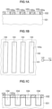
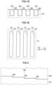
- a mask pattern 102 is formed on a substrate 101 that is made of a crystal and includes a main surface that is the (110) plane (first step).
- the mask pattern 102 includes an opening 103 with a linear portion in a planar view.
- the substrate 101 is made of, for example, a single crystal of silicon.
- the substrate 101 can also be made of a crystal of GaAs or InP.
- the opening 103 has, for example, a rectangular shape in a planar view.
- the opening 103 is formed such that a side surface 103a of a side in the longitudinal direction of a rectangle in a planar view becomes a surface parallel to the facet surface of the substrate 101 made of single crystal silicon, which is tilted by 1° from the (111) plane.
- the longitudinal direction of the above-described rectangle is set to extend in a direction rotated by 1° from the ⁇ 111> direction
- the side surface 103a can be the surface parallel to the facet surface tilted by 1° from the (111) plane.
- the mask pattern 102 is called a line-and-space pattern in which, for example, the plurality of openings 103 form a space pattern.
- the line width can be 200 nm
- the space width can be 200 nm.
- the mask pattern 102 can be formed by a known lithography technique.
- the substrate 101 is etched by etching processing with crystal anisotropy, thereby forming recesses 104 from the main surface of the substrate 101 to the inside of the substrate 101 (second step).
- etching processing with crystal anisotropy can be performed by wet etching using an alkaline solution as an etchant.
- an alkaline solution as an etchant.
- the (111) plane is hardly etched because the etching rate is lower by 1/1000 than on the (100) plane or (110) plane.
- the substrate is etched by an alkaline solution using the mask pattern 102 as a mask
- the (100) plane of the substrate 101 which is exposed to the bottom surface of each opening 103, is etched, and the etching progresses in the thickness direction of the substrate 101.
- side surfaces 105 of the recesses 104 which are formed along with the progress of the etching and are parallel to the side surfaces 103a of the openings 103, are almost (111) planes, and the etching hardly progresses.
- a cross section of the recess 104 perpendicular to the longitudinal direction has a rectangular shape.
- the opening 103 of the mask pattern 102 has a rectangular shape in a planar view
- the opening of the recess 104 has a rectangular shape in a planar view
- the recess 104 is formed into, for example, a rectangular parallelepiped shape.
- etching using an alkaline solution for example, an aqueous solution of potassium hydroxide with a concentration of 33 wt% is used as the alkaline solution, and the etching processing is performed for, for example, about 5 min.
- the mask pattern 102 is removed.
- a standard sample with the recesses 104 formed in the substrate 101 is obtained.
- the recess 104 in this standard sample includes the side surface 105 that forms one plane perpendicular to the main surface of the substrate 101.
- the side surface 105 is a facet surface and is a tilting surface tilted from the (111) plane (for example, tilted by 1°).
- the side surface 105 formed by anisotropic etching is a facet surface tilted from the (111) plane of the single crystal silicon.
- the edge portion of the recess 104 which is formed by the main surface of the substrate 101 and the side surface 105, has a level difference by a step (atomic step) 106 of the side surface 105, as shown in Fig. 2 . If the side surface 105 is tilted by 1° from the (111) plane, the above-described level difference has a size of about 2 nm and periodically occurs at an interval of 120 nm.
- a periodical level difference structure on a nanometer order is formed in the edge portion of the recess 104, which is formed by the main surface of the substrate 101 and the side surface 105.
- This standard sample can be used to calibrate a scanning probe microscope such as an AFM or an electron microscope such as a critical dimension-scanning electron microscope (CD-SEM).
- the size of the level difference by the step 106 changes depending on the angle of tilt from the (111) plane. If the angle of tilt from the (111) plane becomes large, the level difference by the step 106 also becomes large. Hence, the angle of tilt from the (111) plane can be adapted to the desired size of the level difference.
- the substrate 101 is made of a single crystal of silicon has been described above.
- the present invention is not limited to this.
- the substrate 101 can also be made of a crystal of InP or GaAs.
- the side surface 105 can be a tilting surface tilted from the (111)A plane.
- the substrate 101 is made of InP
- an aqueous solution of bromine and hydrobromic acid or an aqueous solution of hydrochloric acid and phosphoric acid can be used as an etchant.
- the (111)A plane of InP is difficult to etch as compared to other crystal surfaces.
- etching processing with crystal anisotropy as described above can be performed, and the recesses 104 can be formed using the mask pattern 102.
- the substrate 101 is made of GaAs
- a liquid mixture of an aqueous ammonia solution and a hydrogen peroxide solution can be used as an etchant.
- the (111)A plane of GaAs is difficult to etch as compared to other crystal surfaces.
- etching processing with crystal anisotropy as described above can be performed, and the recesses 104 can be formed using the mask pattern 102.
- a recess including a side surface that is a facet surface and is a tilting surface tilted from the (111) plane is formed in the substrate whose main surface is the (110) plane. It is therefore possible to provide a standard sample capable of evaluating a line edge roughness on the order of 1 nm.
Landscapes
- General Physics & Mathematics (AREA)
- Physics & Mathematics (AREA)
- Health & Medical Sciences (AREA)
- General Health & Medical Sciences (AREA)
- Nuclear Medicine, Radiotherapy & Molecular Imaging (AREA)
- Radiology & Medical Imaging (AREA)
- Chemical & Material Sciences (AREA)
- Immunology (AREA)
- Biochemistry (AREA)
- Life Sciences & Earth Sciences (AREA)
- Pathology (AREA)
- Analytical Chemistry (AREA)
- Sampling And Sample Adjustment (AREA)
- Engineering & Computer Science (AREA)
- Manufacturing & Machinery (AREA)
- Condensed Matter Physics & Semiconductors (AREA)
- Computer Hardware Design (AREA)
- Microelectronics & Electronic Packaging (AREA)
- Power Engineering (AREA)
- General Chemical & Material Sciences (AREA)
- Chemical Kinetics & Catalysis (AREA)
- Weting (AREA)
- Testing Or Measuring Of Semiconductors Or The Like (AREA)
Claims (6)
- Standardprobe zur Bewertung eines Mikroskops, das Beobachtungen in Nanometergröße durchführen kann, einschließlich eines Rastersondenmikroskops, umfassend:ein Substrat (101) aus einem Kristall mit einer Hauptoberfläche, die eine (110) Ebene ist; und eine Ausnehmung (104), die von der Hauptoberfläche des Substrats (101) bis in ein Inneres des Substrats (101) ausgebildet ist,wobei die Ausnehmung (104) eine Seitenoberfläche (105), die eine Ebene senkrecht zu der Hauptoberfläche des Substrats (101) bildet, und einen Kantenabschnitt umfasst, der durch die Hauptoberfläche des Substrats (101) und die Seitenoberfläche (105) gebildet wird,dadurch gekennzeichnet, dassdie Seitenfläche (105) eine facettierte Oberfläche und eine geneigte Oberfläche ist, die von einer (111)-Ebene geneigt ist, undder Kantenabschnitt eine Struktur mit periodischen Höhenunterschieden in Nanometergröße aufweist.
- Standardprobe gemäß Anspruch 1, wobei das Substrat (101) aus einem Einzelkristall aus Silizium besteht.
- Standardprobe gemäß Anspruch 1, wobei das Substrat (101) aus einem InP-Kristall oder einem GaAs-Kristall besteht.
- Herstellungsverfahren einer Standardprobe, die zur Bewertung eines Mikroskops verwendet wird, das Beobachtungen in Nanometergröße durchführen kann, einschließlich eines Rastersondenmikroskops, umfassend:einen ersten Schritt des Ausbildens eines Maskenmusters (102), umfassend eine Öffnung (103) mit einem in einer ebenen Ansicht linearen Abschnitt, auf einem Substrat (101), das aus einem Kristall mit einer Hauptoberfläche, die eine (110)-Ebene ist, hergestellt ist; undeinem zweiten Schritt des Ätzens des Substrats (101) durch einen Ätzprozess mit Kristallanisotropie unter Verwendung des Maskenmusters (102) als Maske, wodurch eine Ausnehmung (104) gebildet wird, die von der Hauptoberfläche des Substrats (101) zu einem Inneren des Substrats (101) gebildet wird,wobei die Ausnehmung (104) eine Seitenoberfläche (105) umfasst, die eine Ebene senkrecht zu der Hauptoberfläche des Substrats (101) bildet, dadurch gekennzeichnet, dassder zweite Schritt einen Schritt des Ausbildens einer Struktur mit periodischen Höhenunterschieden in Nanometergröße in einem Kantenabschnitt der Ausnehmung (104) umfasst, wobei der Kantenabschnitt durch die Hauptoberfläche des Substrats (101) und die Seitenoberfläche (105) gebildet wird, wobei die Seitenoberfläche (105) eine facettierte Oberfläche und eine geneigte Oberfläche ist, die von einer (111)-Ebene geneigt ist.
- Herstellungsverfahren für die Standardprobe gemäß Anspruch 4, wobei das Substrat (101) aus einem Einzelkristall aus Silizium besteht.
- Herstellungsverfahren für die Standardprobe gemäß Anspruch 4, wobei das Substrat (101) aus einem InP-Kristall oder einem GaAs-Kristall besteht.
Applications Claiming Priority (1)
| Application Number | Priority Date | Filing Date | Title |
|---|---|---|---|
| PCT/JP2020/019260 WO2021229755A1 (ja) | 2020-05-14 | 2020-05-14 | 標準試料およびその作製方法 |
Publications (4)
| Publication Number | Publication Date |
|---|---|
| EP4152011A1 EP4152011A1 (de) | 2023-03-22 |
| EP4152011A4 EP4152011A4 (de) | 2024-01-24 |
| EP4152011C0 EP4152011C0 (de) | 2025-03-12 |
| EP4152011B1 true EP4152011B1 (de) | 2025-03-12 |
Family
ID=78525546
Family Applications (1)
| Application Number | Title | Priority Date | Filing Date |
|---|---|---|---|
| EP20935239.2A Active EP4152011B1 (de) | 2020-05-14 | 2020-05-14 | Standardprobe und verfahren zur herstellung davon |
Country Status (7)
| Country | Link |
|---|---|
| US (1) | US12422453B2 (de) |
| EP (1) | EP4152011B1 (de) |
| JP (1) | JP7390481B2 (de) |
| KR (1) | KR20230002694A (de) |
| CN (1) | CN115552254A (de) |
| TW (1) | TWI863998B (de) |
| WO (1) | WO2021229755A1 (de) |
Family Cites Families (23)
| Publication number | Priority date | Publication date | Assignee | Title |
|---|---|---|---|---|
| JP2649475B2 (ja) * | 1993-04-30 | 1997-09-03 | 住友シチックス株式会社 | 測定精度校正用標準試料とその製造方法 |
| EP0676614B1 (de) * | 1994-04-11 | 2001-06-20 | International Business Machines Corporation | Kalibrierungsnorm für einen Profilometer und Verfahren zu seiner Produktion |
| US5741614A (en) | 1995-10-16 | 1998-04-21 | Nikon Corporation | Atomic force microscope measurement process for dense photoresist patterns |
| KR100300002B1 (ko) | 1998-04-01 | 2001-11-22 | 조동일 | (111)단결정실리콘을이용한마이크로머시닝제조방법 |
| JP2004014856A (ja) | 2002-06-07 | 2004-01-15 | Sharp Corp | 半導体基板の製造方法及び半導体装置の製造方法 |
| US6869480B1 (en) * | 2002-07-17 | 2005-03-22 | The United States Of America As Represented By The United States National Aeronautics And Space Administration | Method for the production of nanometer scale step height reference specimens |
| JP4287671B2 (ja) * | 2003-02-19 | 2009-07-01 | 株式会社日立ハイテクノロジーズ | 測長用標準部材およびその作製方法、並びにそれを用いた電子ビーム測長装置 |
| US20050116290A1 (en) | 2003-12-02 | 2005-06-02 | De Souza Joel P. | Planar substrate with selected semiconductor crystal orientations formed by localized amorphization and recrystallization of stacked template layers |
| JP2005291859A (ja) * | 2004-03-31 | 2005-10-20 | Nec Compound Semiconductor Devices Ltd | 微細構造測定方法、微細構造測定装置、および、微細構造解析システム |
| KR100849177B1 (ko) | 2005-01-04 | 2008-07-30 | 삼성전자주식회사 | 패싯 채널들을 갖는 모스 트랜지스터를 채택하는 반도체집적회로 소자들 및 그 제조방법들 |
| JP2006220517A (ja) * | 2005-02-10 | 2006-08-24 | National Institute For Materials Science | 校正試料の作製方法 |
| JP4803440B2 (ja) | 2005-08-16 | 2011-10-26 | 独立行政法人産業技術総合研究所 | 探針形状評価用標準試料 |
| JP2008224258A (ja) * | 2007-03-09 | 2008-09-25 | Hitachi High-Technologies Corp | 荷電粒子線装置 |
| JP4287891B2 (ja) * | 2007-12-20 | 2009-07-01 | 株式会社日立ハイテクノロジーズ | 測長用標準部材及びそれを用いた電子ビーム測長装置 |
| US8373113B2 (en) * | 2008-11-05 | 2013-02-12 | Hitachi High-Technologies Corporation | Calibration standard member, method for manufacturing the member and scanning electronic microscope using the member |
| JP5400474B2 (ja) * | 2009-05-22 | 2014-01-29 | 株式会社日立ハイテクノロジーズ | 電子顕微鏡装置の寸法校正用標準部材、その製造方法、およびそれを用いた電子顕微鏡装置の校正方法 |
| JP5794648B2 (ja) * | 2011-11-11 | 2015-10-14 | 学校法人関西学院 | ナノメーター標準原器及びナノメーター標準原器の製造方法 |
| JP5764046B2 (ja) | 2011-11-21 | 2015-08-12 | 住友電気工業株式会社 | 炭化珪素半導体装置の製造方法 |
| TW201535720A (zh) * | 2014-03-07 | 2015-09-16 | Visual Photonics Epitaxy Co Ltd | 定向磊晶之異質接面雙極性電晶體結構 |
| ITUA20163703A1 (it) * | 2016-05-23 | 2017-11-23 | Istituto Naz Di Ricerca Metrologica | Dispositivo campione di riferimento per la calibrazione di misure di lunghezza e relativo procedimento di calibrazione |
| US11251302B2 (en) * | 2017-09-27 | 2022-02-15 | Intel Corporation | Epitaxial oxide plug for strained transistors |
| JP2019078578A (ja) | 2017-10-23 | 2019-05-23 | 株式会社日立ハイテクノロジーズ | パターン計測方法、パターン計測装置、及びコンピュータープログラム |
| JP7267882B2 (ja) * | 2019-09-17 | 2023-05-02 | キオクシア株式会社 | 基板、パターン、及び計測装置の較正方法 |
-
2020
- 2020-05-14 WO PCT/JP2020/019260 patent/WO2021229755A1/ja not_active Ceased
- 2020-05-14 US US17/998,324 patent/US12422453B2/en active Active
- 2020-05-14 JP JP2022522439A patent/JP7390481B2/ja active Active
- 2020-05-14 CN CN202080100681.2A patent/CN115552254A/zh active Pending
- 2020-05-14 KR KR1020227039628A patent/KR20230002694A/ko active Pending
- 2020-05-14 EP EP20935239.2A patent/EP4152011B1/de active Active
- 2020-05-21 TW TW109116928A patent/TWI863998B/zh active
Also Published As
| Publication number | Publication date |
|---|---|
| JP7390481B2 (ja) | 2023-12-01 |
| KR20230002694A (ko) | 2023-01-05 |
| EP4152011A1 (de) | 2023-03-22 |
| JPWO2021229755A1 (de) | 2021-11-18 |
| TWI863998B (zh) | 2024-12-01 |
| CN115552254A (zh) | 2022-12-30 |
| EP4152011A4 (de) | 2024-01-24 |
| US12422453B2 (en) | 2025-09-23 |
| EP4152011C0 (de) | 2025-03-12 |
| WO2021229755A1 (ja) | 2021-11-18 |
| US20230228792A1 (en) | 2023-07-20 |
| TW202142867A (zh) | 2021-11-16 |
Similar Documents
| Publication | Publication Date | Title |
|---|---|---|
| JP4971050B2 (ja) | 半導体装置の寸法測定装置 | |
| CN112949236B (zh) | 刻蚀偏差的计算方法以及计算系统 | |
| Volk et al. | Linear standard for SEM–AFM microelectronics dimensional metrology in the range 0.01–100 μm | |
| KR100367535B1 (ko) | 집적회로제조방법 | |
| US7210330B2 (en) | Methods of fabricating structures for characterizing tip shape of scanning probe microscope probes and structures fabricated thereby | |
| US5684301A (en) | Monocrystalline test structures, and use for calibrating instruments | |
| US10950439B2 (en) | Pattern forming method | |
| JP2019056726A (ja) | 炭化珪素半導体基板およびそれを用いた炭化珪素半導体装置の製造方法 | |
| EP4152011B1 (de) | Standardprobe und verfahren zur herstellung davon | |
| Armstrong et al. | Fabrication of uniform, periodic arrays of exotic AlN nanoholes by combining dry etching and hot selective wet etching, accessing geometries unrealisable from wet etching of planar AlN | |
| HK40085427A (en) | Standard sample and manufacturing method thereof | |
| Foucher et al. | CD-AFM versus CD-SEM for resist LER and LWR measurements | |
| KR102731521B1 (ko) | 5nm이하 Si 나노 구조체 표준 물질 및 이의 제조 방법 | |
| JP7267882B2 (ja) | 基板、パターン、及び計測装置の較正方法 | |
| JP2009076863A (ja) | 半導体装置の製造方法 | |
| KR20080006911A (ko) | 원자간력 현미경용 캔틸레버 탐침 및 그의 제조방법 | |
| JP5035797B2 (ja) | 探針形成用エッチングマスク及びそれを用いた探針の製造方法 | |
| CN119008442B (zh) | 一种测量数据模型的建立方法、测量方法及工艺控制方法 | |
| Lagerquist et al. | Improving SEM linewidth metrology by two-dimensional scanning force microscopy | |
| JP3284514B2 (ja) | 微細寸法標準構造及び微細寸法標準化方法 | |
| US20230275033A1 (en) | Semiconductor substrate having an alignment structure | |
| EP4511699B1 (de) | Verfahren und system zur erkennung und/oder quantifizierung von fertigungsungenauigkeiten | |
| JP4013727B2 (ja) | バーニアパターン及びそれを用いたマスク合わせ方法、パターン測長方法 | |
| KR100677035B1 (ko) | 미세 패턴의 임계 치수 및 측벽 경사 각도 측정 방법 | |
| CN119937263A (zh) | 一种零层光刻对准标记的制作方法及半导体结构 |
Legal Events
| Date | Code | Title | Description |
|---|---|---|---|
| STAA | Information on the status of an ep patent application or granted ep patent |
Free format text: STATUS: THE INTERNATIONAL PUBLICATION HAS BEEN MADE |
|
| PUAI | Public reference made under article 153(3) epc to a published international application that has entered the european phase |
Free format text: ORIGINAL CODE: 0009012 |
|
| STAA | Information on the status of an ep patent application or granted ep patent |
Free format text: STATUS: REQUEST FOR EXAMINATION WAS MADE |
|
| 17P | Request for examination filed |
Effective date: 20221108 |
|
| AK | Designated contracting states |
Kind code of ref document: A1 Designated state(s): AL AT BE BG CH CY CZ DE DK EE ES FI FR GB GR HR HU IE IS IT LI LT LU LV MC MK MT NL NO PL PT RO RS SE SI SK SM TR |
|
| DAV | Request for validation of the european patent (deleted) | ||
| DAX | Request for extension of the european patent (deleted) | ||
| A4 | Supplementary search report drawn up and despatched |
Effective date: 20231222 |
|
| RIC1 | Information provided on ipc code assigned before grant |
Ipc: G01N 1/28 20060101ALI20231218BHEP Ipc: G01Q 40/02 20100101AFI20231218BHEP |
|
| GRAP | Despatch of communication of intention to grant a patent |
Free format text: ORIGINAL CODE: EPIDOSNIGR1 |
|
| STAA | Information on the status of an ep patent application or granted ep patent |
Free format text: STATUS: GRANT OF PATENT IS INTENDED |
|
| INTG | Intention to grant announced |
Effective date: 20241004 |
|
| GRAS | Grant fee paid |
Free format text: ORIGINAL CODE: EPIDOSNIGR3 |
|
| GRAA | (expected) grant |
Free format text: ORIGINAL CODE: 0009210 |
|
| STAA | Information on the status of an ep patent application or granted ep patent |
Free format text: STATUS: THE PATENT HAS BEEN GRANTED |
|
| AK | Designated contracting states |
Kind code of ref document: B1 Designated state(s): AL AT BE BG CH CY CZ DE DK EE ES FI FR GB GR HR HU IE IS IT LI LT LU LV MC MK MT NL NO PL PT RO RS SE SI SK SM TR |
|
| REG | Reference to a national code |
Ref country code: GB Ref legal event code: FG4D |
|
| REG | Reference to a national code |
Ref country code: CH Ref legal event code: EP |
|
| REG | Reference to a national code |
Ref country code: DE Ref legal event code: R096 Ref document number: 602020047778 Country of ref document: DE |
|
| REG | Reference to a national code |
Ref country code: IE Ref legal event code: FG4D |
|
| U01 | Request for unitary effect filed |
Effective date: 20250402 |
|
| U07 | Unitary effect registered |
Designated state(s): AT BE BG DE DK EE FI FR IT LT LU LV MT NL PT RO SE SI Effective date: 20250409 |
|
| U20 | Renewal fee for the european patent with unitary effect paid |
Year of fee payment: 6 Effective date: 20250520 |
|
| PG25 | Lapsed in a contracting state [announced via postgrant information from national office to epo] |
Ref country code: RS Free format text: LAPSE BECAUSE OF FAILURE TO SUBMIT A TRANSLATION OF THE DESCRIPTION OR TO PAY THE FEE WITHIN THE PRESCRIBED TIME-LIMIT Effective date: 20250612 |
|
| PG25 | Lapsed in a contracting state [announced via postgrant information from national office to epo] |
Ref country code: ES Free format text: LAPSE BECAUSE OF FAILURE TO SUBMIT A TRANSLATION OF THE DESCRIPTION OR TO PAY THE FEE WITHIN THE PRESCRIBED TIME-LIMIT Effective date: 20250312 |
|
| PGFP | Annual fee paid to national office [announced via postgrant information from national office to epo] |
Ref country code: GB Payment date: 20250602 Year of fee payment: 6 |
|
| PG25 | Lapsed in a contracting state [announced via postgrant information from national office to epo] |
Ref country code: NO Free format text: LAPSE BECAUSE OF FAILURE TO SUBMIT A TRANSLATION OF THE DESCRIPTION OR TO PAY THE FEE WITHIN THE PRESCRIBED TIME-LIMIT Effective date: 20250612 |
|
| PG25 | Lapsed in a contracting state [announced via postgrant information from national office to epo] |
Ref country code: HR Free format text: LAPSE BECAUSE OF FAILURE TO SUBMIT A TRANSLATION OF THE DESCRIPTION OR TO PAY THE FEE WITHIN THE PRESCRIBED TIME-LIMIT Effective date: 20250312 |
|
| PG25 | Lapsed in a contracting state [announced via postgrant information from national office to epo] |
Ref country code: GR Free format text: LAPSE BECAUSE OF FAILURE TO SUBMIT A TRANSLATION OF THE DESCRIPTION OR TO PAY THE FEE WITHIN THE PRESCRIBED TIME-LIMIT Effective date: 20250613 |
|
| PGFP | Annual fee paid to national office [announced via postgrant information from national office to epo] |
Ref country code: CH Payment date: 20250601 Year of fee payment: 6 |
|
| PG25 | Lapsed in a contracting state [announced via postgrant information from national office to epo] |
Ref country code: SM Free format text: LAPSE BECAUSE OF FAILURE TO SUBMIT A TRANSLATION OF THE DESCRIPTION OR TO PAY THE FEE WITHIN THE PRESCRIBED TIME-LIMIT Effective date: 20250312 |
|
| PG25 | Lapsed in a contracting state [announced via postgrant information from national office to epo] |
Ref country code: PL Free format text: LAPSE BECAUSE OF FAILURE TO SUBMIT A TRANSLATION OF THE DESCRIPTION OR TO PAY THE FEE WITHIN THE PRESCRIBED TIME-LIMIT Effective date: 20250312 |
|
| PG25 | Lapsed in a contracting state [announced via postgrant information from national office to epo] |
Ref country code: CZ Free format text: LAPSE BECAUSE OF FAILURE TO SUBMIT A TRANSLATION OF THE DESCRIPTION OR TO PAY THE FEE WITHIN THE PRESCRIBED TIME-LIMIT Effective date: 20250312 |
|
| PG25 | Lapsed in a contracting state [announced via postgrant information from national office to epo] |
Ref country code: SK Free format text: LAPSE BECAUSE OF FAILURE TO SUBMIT A TRANSLATION OF THE DESCRIPTION OR TO PAY THE FEE WITHIN THE PRESCRIBED TIME-LIMIT Effective date: 20250312 |
|
| PG25 | Lapsed in a contracting state [announced via postgrant information from national office to epo] |
Ref country code: IS Free format text: LAPSE BECAUSE OF FAILURE TO SUBMIT A TRANSLATION OF THE DESCRIPTION OR TO PAY THE FEE WITHIN THE PRESCRIBED TIME-LIMIT Effective date: 20250712 |
|
| PLBE | No opposition filed within time limit |
Free format text: ORIGINAL CODE: 0009261 |
|
| STAA | Information on the status of an ep patent application or granted ep patent |
Free format text: STATUS: NO OPPOSITION FILED WITHIN TIME LIMIT |
|
| REG | Reference to a national code |
Ref country code: CH Ref legal event code: L10 Free format text: ST27 STATUS EVENT CODE: U-0-0-L10-L00 (AS PROVIDED BY THE NATIONAL OFFICE) Effective date: 20260121 |
|
| PG25 | Lapsed in a contracting state [announced via postgrant information from national office to epo] |
Ref country code: MC Free format text: LAPSE BECAUSE OF FAILURE TO SUBMIT A TRANSLATION OF THE DESCRIPTION OR TO PAY THE FEE WITHIN THE PRESCRIBED TIME-LIMIT Effective date: 20250312 |