EP4152011B1 - Standard sample and method for producing same - Google Patents
Standard sample and method for producing same Download PDFInfo
- Publication number
- EP4152011B1 EP4152011B1 EP20935239.2A EP20935239A EP4152011B1 EP 4152011 B1 EP4152011 B1 EP 4152011B1 EP 20935239 A EP20935239 A EP 20935239A EP 4152011 B1 EP4152011 B1 EP 4152011B1
- Authority
- EP
- European Patent Office
- Prior art keywords
- substrate
- standard sample
- plane
- crystal
- main surface
- Prior art date
- Legal status (The legal status is an assumption and is not a legal conclusion. Google has not performed a legal analysis and makes no representation as to the accuracy of the status listed.)
- Active
Links
Images
Classifications
-
- G—PHYSICS
- G01—MEASURING; TESTING
- G01N—INVESTIGATING OR ANALYSING MATERIALS BY DETERMINING THEIR CHEMICAL OR PHYSICAL PROPERTIES
- G01N1/00—Sampling; Preparing specimens for investigation
- G01N1/28—Preparing specimens for investigation including physical details of (bio-)chemical methods covered elsewhere, e.g. G01N33/50, C12Q
-
- G—PHYSICS
- G01—MEASURING; TESTING
- G01Q—SCANNING-PROBE TECHNIQUES OR APPARATUS; APPLICATIONS OF SCANNING-PROBE TECHNIQUES, e.g. SCANNING PROBE MICROSCOPY [SPM]
- G01Q40/00—Calibration, e.g. of probes
- G01Q40/02—Calibration standards and methods of fabrication thereof
-
- H—ELECTRICITY
- H10—SEMICONDUCTOR DEVICES; ELECTRIC SOLID-STATE DEVICES NOT OTHERWISE PROVIDED FOR
- H10P—GENERIC PROCESSES OR APPARATUS FOR THE MANUFACTURE OR TREATMENT OF DEVICES COVERED BY CLASS H10
- H10P50/00—Etching of wafers, substrates or parts of devices
- H10P50/69—Etching of wafers, substrates or parts of devices using masks for semiconductor materials
- H10P50/691—Etching of wafers, substrates or parts of devices using masks for semiconductor materials for Group V materials or Group III-V materials
-
- G—PHYSICS
- G01—MEASURING; TESTING
- G01N—INVESTIGATING OR ANALYSING MATERIALS BY DETERMINING THEIR CHEMICAL OR PHYSICAL PROPERTIES
- G01N1/00—Sampling; Preparing specimens for investigation
- G01N1/28—Preparing specimens for investigation including physical details of (bio-)chemical methods covered elsewhere, e.g. G01N33/50, C12Q
- G01N2001/2893—Preparing calibration standards
-
- H—ELECTRICITY
- H10—SEMICONDUCTOR DEVICES; ELECTRIC SOLID-STATE DEVICES NOT OTHERWISE PROVIDED FOR
- H10P—GENERIC PROCESSES OR APPARATUS FOR THE MANUFACTURE OR TREATMENT OF DEVICES COVERED BY CLASS H10
- H10P50/00—Etching of wafers, substrates or parts of devices
- H10P50/60—Wet etching
- H10P50/64—Wet etching of semiconductor materials
- H10P50/642—Chemical etching
- H10P50/644—Anisotropic liquid etching
-
- H—ELECTRICITY
- H10—SEMICONDUCTOR DEVICES; ELECTRIC SOLID-STATE DEVICES NOT OTHERWISE PROVIDED FOR
- H10P—GENERIC PROCESSES OR APPARATUS FOR THE MANUFACTURE OR TREATMENT OF DEVICES COVERED BY CLASS H10
- H10P50/00—Etching of wafers, substrates or parts of devices
- H10P50/69—Etching of wafers, substrates or parts of devices using masks for semiconductor materials
- H10P50/691—Etching of wafers, substrates or parts of devices using masks for semiconductor materials for Group V materials or Group III-V materials
- H10P50/693—Etching of wafers, substrates or parts of devices using masks for semiconductor materials for Group V materials or Group III-V materials characterised by their size, orientation, disposition, behaviour or shape, in horizontal or vertical plane
Definitions
- the present invention relates to a standard sample used to evaluate a scanning probe microscope or the like and a manufacturing method thereof.
- the road map IRDS International Roadmap for Device and System
- 2017 specifies goals of a pattern size in a logic device until 2021, in which a half pitch is 12 nm, and a line edge roughness (LER) is less than 2 nm, and pattern manufacturing methods and inspection methods for the goals have been discussed.
- LER represents the unevenness of the edge of a resist pattern used as a mask in a lithography technique.
- LER evaluation method measurement using a microscope capable of performing observation in a nanometer size (having a resolution in a nanometer size), such as an atomic force microscope (AFM), can be used.
- AFM atomic force microscope
- to accurately measure roughness using an image output from a measurement device such as a SEM noise included in an image signal is removed (see Patent literature 1).
- a standard sample whose LER is controlled in advance is used.
- the AIST conducts certifications for structures of 10 nm or more, no technique is specified yet concerning how to correctly measure a shape whose size is on the order of 1 nm.
- JP2004251682A describes a semiconductor member having a pattern made of an array of first diffraction gratings and also including an array of second diffraction gratings different from the first diffraction grating in a predetermined cycle.
- the above-described standard sample is manufactured using, for example, semiconductor device manufacturing techniques such as a deposition technique, a lithography technique, and an etching technique.
- semiconductor device manufacturing techniques such as a deposition technique, a lithography technique, and an etching technique.
- an LER with a nanometer size is generated in the edge portion of the pattern, and it is difficult to clarify the difference from a defect with a nanometer size. For this reason, it is not sufficient as a standard sample.
- the present invention has been made to solve the above-described problem, and has as its object to provide a standard sample capable of evaluating a line edge roughness on the order of 1 nm.
- a standard sample used to evaluate a microscope capable of performing observation in a nanometer size including a scanning probe microscope, comprising a substrate made of a crystal with a main surface that is a (110) plane, and a recess formed from the main surface of the substrate to an inside of the substrate, wherein the recess includes a side surface that forms one plane perpendicular to the main surface of the substrate, and the side surface is a facet surface and is a tilting surface tilted from a (111) plane.
- a manufacturing method of a standard sample used to evaluate a microscope capable of performing observation in a nanometer size including a scanning probe microscope, comprising a first step of forming a mask pattern including an opening with a linear portion in a planar view on a substrate made of a crystal with a main surface that is a (110) plane, and a second step of etching the substrate by etching processing with crystal anisotropy using the mask pattern as a mask, thereby forming a recess formed from the main surface of the substrate to an inside of the substrate, wherein the recess includes a side surface that forms one plane perpendicular to the main surface of the substrate, and the side surface is a facet surface and is a tilting surface tilted from a (111) plane.
- a recess including a side surface that is a facet surface and is a tilting surface tilted from the (111) plane is formed in a substrate whose main surface is the (110) plane, it is possible to provide a standard sample capable of evaluating a line edge roughness on the order of 1 nm.
- This manufacturing method is a manufacturing method of a standard sample used to evaluate a microscope capable of performing observation in a nanometer size (having a resolution in a nanometer size), including a scanning probe microscope.
- a mask pattern 102 is formed on a substrate 101 that is made of a crystal and includes a main surface that is the (110) plane (first step).
- the mask pattern 102 includes an opening 103 with a linear portion in a planar view.
- the substrate 101 is made of, for example, a single crystal of silicon.
- the substrate 101 can also be made of a crystal of GaAs or InP.
- the opening 103 has, for example, a rectangular shape in a planar view.
- the opening 103 is formed such that a side surface 103a of a side in the longitudinal direction of a rectangle in a planar view becomes a surface parallel to the facet surface of the substrate 101 made of single crystal silicon, which is tilted by 1° from the (111) plane.
- the longitudinal direction of the above-described rectangle is set to extend in a direction rotated by 1° from the ⁇ 111> direction
- the side surface 103a can be the surface parallel to the facet surface tilted by 1° from the (111) plane.
- the mask pattern 102 is called a line-and-space pattern in which, for example, the plurality of openings 103 form a space pattern.
- the line width can be 200 nm
- the space width can be 200 nm.
- the mask pattern 102 can be formed by a known lithography technique.
- the substrate 101 is etched by etching processing with crystal anisotropy, thereby forming recesses 104 from the main surface of the substrate 101 to the inside of the substrate 101 (second step).
- etching processing with crystal anisotropy can be performed by wet etching using an alkaline solution as an etchant.
- an alkaline solution as an etchant.
- the (111) plane is hardly etched because the etching rate is lower by 1/1000 than on the (100) plane or (110) plane.
- the substrate is etched by an alkaline solution using the mask pattern 102 as a mask
- the (100) plane of the substrate 101 which is exposed to the bottom surface of each opening 103, is etched, and the etching progresses in the thickness direction of the substrate 101.
- side surfaces 105 of the recesses 104 which are formed along with the progress of the etching and are parallel to the side surfaces 103a of the openings 103, are almost (111) planes, and the etching hardly progresses.
- a cross section of the recess 104 perpendicular to the longitudinal direction has a rectangular shape.
- the opening 103 of the mask pattern 102 has a rectangular shape in a planar view
- the opening of the recess 104 has a rectangular shape in a planar view
- the recess 104 is formed into, for example, a rectangular parallelepiped shape.
- etching using an alkaline solution for example, an aqueous solution of potassium hydroxide with a concentration of 33 wt% is used as the alkaline solution, and the etching processing is performed for, for example, about 5 min.
- the mask pattern 102 is removed.
- a standard sample with the recesses 104 formed in the substrate 101 is obtained.
- the recess 104 in this standard sample includes the side surface 105 that forms one plane perpendicular to the main surface of the substrate 101.
- the side surface 105 is a facet surface and is a tilting surface tilted from the (111) plane (for example, tilted by 1°).
- the side surface 105 formed by anisotropic etching is a facet surface tilted from the (111) plane of the single crystal silicon.
- the edge portion of the recess 104 which is formed by the main surface of the substrate 101 and the side surface 105, has a level difference by a step (atomic step) 106 of the side surface 105, as shown in Fig. 2 . If the side surface 105 is tilted by 1° from the (111) plane, the above-described level difference has a size of about 2 nm and periodically occurs at an interval of 120 nm.
- a periodical level difference structure on a nanometer order is formed in the edge portion of the recess 104, which is formed by the main surface of the substrate 101 and the side surface 105.
- This standard sample can be used to calibrate a scanning probe microscope such as an AFM or an electron microscope such as a critical dimension-scanning electron microscope (CD-SEM).
- the size of the level difference by the step 106 changes depending on the angle of tilt from the (111) plane. If the angle of tilt from the (111) plane becomes large, the level difference by the step 106 also becomes large. Hence, the angle of tilt from the (111) plane can be adapted to the desired size of the level difference.
- the substrate 101 is made of a single crystal of silicon has been described above.
- the present invention is not limited to this.
- the substrate 101 can also be made of a crystal of InP or GaAs.
- the side surface 105 can be a tilting surface tilted from the (111)A plane.
- the substrate 101 is made of InP
- an aqueous solution of bromine and hydrobromic acid or an aqueous solution of hydrochloric acid and phosphoric acid can be used as an etchant.
- the (111)A plane of InP is difficult to etch as compared to other crystal surfaces.
- etching processing with crystal anisotropy as described above can be performed, and the recesses 104 can be formed using the mask pattern 102.
- the substrate 101 is made of GaAs
- a liquid mixture of an aqueous ammonia solution and a hydrogen peroxide solution can be used as an etchant.
- the (111)A plane of GaAs is difficult to etch as compared to other crystal surfaces.
- etching processing with crystal anisotropy as described above can be performed, and the recesses 104 can be formed using the mask pattern 102.
- a recess including a side surface that is a facet surface and is a tilting surface tilted from the (111) plane is formed in the substrate whose main surface is the (110) plane. It is therefore possible to provide a standard sample capable of evaluating a line edge roughness on the order of 1 nm.
Landscapes
- Physics & Mathematics (AREA)
- Health & Medical Sciences (AREA)
- General Health & Medical Sciences (AREA)
- General Physics & Mathematics (AREA)
- Nuclear Medicine, Radiotherapy & Molecular Imaging (AREA)
- Radiology & Medical Imaging (AREA)
- Life Sciences & Earth Sciences (AREA)
- Chemical & Material Sciences (AREA)
- Analytical Chemistry (AREA)
- Biochemistry (AREA)
- Immunology (AREA)
- Pathology (AREA)
- Sampling And Sample Adjustment (AREA)
- Weting (AREA)
- Testing Or Measuring Of Semiconductors Or The Like (AREA)
Description
- The present invention relates to a standard sample used to evaluate a scanning probe microscope or the like and a manufacturing method thereof.
- Concerning semiconductor micronization, the road map IRDS (International Roadmap for Device and System) formulated in 2017 by IEEE specifies goals of a pattern size in a logic device until 2021, in which a half pitch is 12 nm, and a line edge roughness (LER) is less than 2 nm, and pattern manufacturing methods and inspection methods for the goals have been discussed. Note that the LER represents the unevenness of the edge of a resist pattern used as a mask in a lithography technique.
- As an LER evaluation method, measurement using a microscope capable of performing observation in a nanometer size (having a resolution in a nanometer size), such as an atomic force microscope (AFM), can be used. In measurement of this type, to accurately measure roughness using an image output from a measurement device such as a SEM, noise included in an image signal is removed (see Patent literature 1). In this technique, to remove noise included in the image signal, a standard sample whose LER is controlled in advance is used.
- Also, in a measurement technique such as AFM, to guarantee a resolution or an error, measurement by a probe in a nanometer size is executed using a standard sample whose minimum structure has a size of 100 nm or less, and the resolution is obtained from obtained image data (see Patent literature 2). In this standard sample, however, although the size is decided, the shape of the pattern edge is indefinite.
- On the other hand, as a currently used standard sample, a standard sample prepared by the NIST (the National Institute of Standards and Technology) in U.S.A. is used. This standard sample is a nanowire with a minimum size of 130 nm.
- In Japan, the National Institute of Advanced Industrial Science and Technology (AIST) conducts certifications in the length direction using a tungstendot array. However, the minimum size of this standard sample is 119 nm, which is not small enough to evaluate presently problematic unevenness on several nm order.
- Also, although the AIST conducts certifications for structures of 10 nm or more, no technique is specified yet concerning how to correctly measure a shape whose size is on the order of 1 nm.
-
- Patent Literature 1:
Japanese Patent Laid-Open No. 2019-078578 - Patent Literature 2:
Japanese Patent Laid-Open No. 2007-078679 - Further,
JP2004251682A - It is considered that the above-described standard sample is manufactured using, for example, semiconductor device manufacturing techniques such as a deposition technique, a lithography technique, and an etching technique. However, in a periodical pattern formed by these manufacturing methods, an LER with a nanometer size is generated in the edge portion of the pattern, and it is difficult to clarify the difference from a defect with a nanometer size. For this reason, it is not sufficient as a standard sample.
- The present invention has been made to solve the above-described problem, and has as its object to provide a standard sample capable of evaluating a line edge roughness on the order of 1 nm. Means of Solution to the Problem
- According to claim 1 of the present invention, there is provided a standard sample used to evaluate a microscope capable of performing observation in a nanometer size, including a scanning probe microscope, comprising a substrate made of a crystal with a main surface that is a (110) plane, and a recess formed from the main surface of the substrate to an inside of the substrate, wherein the recess includes a side surface that forms one plane perpendicular to the main surface of the substrate, and the side surface is a facet surface and is a tilting surface tilted from a (111) plane.
- According to claim 4 of the present invention, there is also provided a manufacturing method of a standard sample used to evaluate a microscope capable of performing observation in a nanometer size, including a scanning probe microscope, comprising a first step of forming a mask pattern including an opening with a linear portion in a planar view on a substrate made of a crystal with a main surface that is a (110) plane, and a second step of etching the substrate by etching processing with crystal anisotropy using the mask pattern as a mask, thereby forming a recess formed from the main surface of the substrate to an inside of the substrate, wherein the recess includes a side surface that forms one plane perpendicular to the main surface of the substrate, and the side surface is a facet surface and is a tilting surface tilted from a (111) plane.
- As described above, according to the present invention, since a recess including a side surface that is a facet surface and is a tilting surface tilted from the (111) plane is formed in a substrate whose main surface is the (110) plane, it is possible to provide a standard sample capable of evaluating a line edge roughness on the order of 1 nm.
-
-
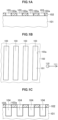
Fig. 1A is a sectional view showing a state of a standard sample in a midway step so as to explain the manufacturing method of the standard sample according to the embodiment of the present invention; -
Fig. 1B is a plan view showing a state of the standard sample in a midway step so as to explain the manufacturing method of the standard sample according to the embodiment of the present invention; -
Fig. 1C is a sectional view showing a state of the standard sample in a midway step so as to explain the manufacturing method of the standard sample according to the embodiment of the present invention; -
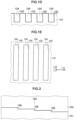
Fig. 1D is a sectional view showing a state of the standard sample in a midway step so as to explain the manufacturing method of the standard sample according to the embodiment of the present invention; -
Fig. 1E is a plan view showing a state of the standard sample in a midway step so as to explain the manufacturing method of the standard sample according to the embodiment of the present invention; and -
Fig. 2 is a plan view showing the structure of a part of the standard sample according to the embodiment of the present invention. - A manufacturing method of a standard sample according to the embodiment of the present invention will now be described with reference to
Figs. 1A to 1E . This manufacturing method is a manufacturing method of a standard sample used to evaluate a microscope capable of performing observation in a nanometer size (having a resolution in a nanometer size), including a scanning probe microscope. - First, as shown in
Figs. 1A and 1B , amask pattern 102 is formed on asubstrate 101 that is made of a crystal and includes a main surface that is the (110) plane (first step). Themask pattern 102 includes anopening 103 with a linear portion in a planar view. Thesubstrate 101 is made of, for example, a single crystal of silicon. Thesubstrate 101 can also be made of a crystal of GaAs or InP. The opening 103 has, for example, a rectangular shape in a planar view. For example, theopening 103 is formed such that aside surface 103a of a side in the longitudinal direction of a rectangle in a planar view becomes a surface parallel to the facet surface of thesubstrate 101 made of single crystal silicon, which is tilted by 1° from the (111) plane. For example, if the longitudinal direction of the above-described rectangle is set to extend in a direction rotated by 1° from the <111> direction, theside surface 103a can be the surface parallel to the facet surface tilted by 1° from the (111) plane. - A plurality of
openings 103 are formed. Themask pattern 102 is called a line-and-space pattern in which, for example, the plurality ofopenings 103 form a space pattern. For example, the line width can be 200 nm, and the space width can be 200 nm. For example, themask pattern 102 can be formed by a known lithography technique. - Next, as shown in
Fig. 1C , using themask pattern 102 as a mask, thesubstrate 101 is etched by etching processing with crystal anisotropy, thereby formingrecesses 104 from the main surface of thesubstrate 101 to the inside of the substrate 101 (second step). For example, for thesubstrate 101 made of single crystal silicon, etching processing with crystal anisotropy can be performed by wet etching using an alkaline solution as an etchant. As is well known, if single crystal silicon is etched using an alkaline solution, the (111) plane is hardly etched because the etching rate is lower by 1/1000 than on the (100) plane or (110) plane. - Hence, if the substrate is etched by an alkaline solution using the
mask pattern 102 as a mask, the (100) plane of thesubstrate 101, which is exposed to the bottom surface of eachopening 103, is etched, and the etching progresses in the thickness direction of thesubstrate 101. On the other hand,side surfaces 105 of therecesses 104, which are formed along with the progress of the etching and are parallel to theside surfaces 103a of theopenings 103, are almost (111) planes, and the etching hardly progresses. As a result, a cross section of therecess 104 perpendicular to the longitudinal direction has a rectangular shape. Note that since theopening 103 of themask pattern 102 has a rectangular shape in a planar view, the opening of therecess 104 has a rectangular shape in a planar view, and therecess 104 is formed into, for example, a rectangular parallelepiped shape. - Note that in the above-described etching using an alkaline solution, for example, an aqueous solution of potassium hydroxide with a concentration of 33 wt% is used as the alkaline solution, and the etching processing is performed for, for example, about 5 min. After the
recesses 104 are formed in this way, themask pattern 102 is removed. Then, as shown inFigs. 1D and 1E , a standard sample with therecesses 104 formed in thesubstrate 101 is obtained. Therecess 104 in this standard sample includes theside surface 105 that forms one plane perpendicular to the main surface of thesubstrate 101. Theside surface 105 is a facet surface and is a tilting surface tilted from the (111) plane (for example, tilted by 1°). - As described above, the
side surface 105 formed by anisotropic etching is a facet surface tilted from the (111) plane of the single crystal silicon. For this reason, the edge portion of therecess 104, which is formed by the main surface of thesubstrate 101 and theside surface 105, has a level difference by a step (atomic step) 106 of theside surface 105, as shown inFig. 2 . If theside surface 105 is tilted by 1° from the (111) plane, the above-described level difference has a size of about 2 nm and periodically occurs at an interval of 120 nm. Hence, a periodical level difference structure on a nanometer order is formed in the edge portion of therecess 104, which is formed by the main surface of thesubstrate 101 and theside surface 105. This standard sample can be used to calibrate a scanning probe microscope such as an AFM or an electron microscope such as a critical dimension-scanning electron microscope (CD-SEM). - Note that the size of the level difference by the
step 106 changes depending on the angle of tilt from the (111) plane. If the angle of tilt from the (111) plane becomes large, the level difference by thestep 106 also becomes large. Hence, the angle of tilt from the (111) plane can be adapted to the desired size of the level difference. - A case where the
substrate 101 is made of a single crystal of silicon has been described above. However, the present invention is not limited to this. Thesubstrate 101 can also be made of a crystal of InP or GaAs. In this case, theside surface 105 can be a tilting surface tilted from the (111)A plane. - For example, if the
substrate 101 is made of InP, an aqueous solution of bromine and hydrobromic acid or an aqueous solution of hydrochloric acid and phosphoric acid can be used as an etchant. In this wet etching, the (111)A plane of InP is difficult to etch as compared to other crystal surfaces. Hence, etching processing with crystal anisotropy as described above can be performed, and therecesses 104 can be formed using themask pattern 102. - Also, if the
substrate 101 is made of GaAs, a liquid mixture of an aqueous ammonia solution and a hydrogen peroxide solution can be used as an etchant. In this wet etching as well, the (111)A plane of GaAs is difficult to etch as compared to other crystal surfaces. Hence, etching processing with crystal anisotropy as described above can be performed, and therecesses 104 can be formed using themask pattern 102. - As described above, according to the present invention, a recess including a side surface that is a facet surface and is a tilting surface tilted from the (111) plane is formed in the substrate whose main surface is the (110) plane. It is therefore possible to provide a standard sample capable of evaluating a line edge roughness on the order of 1 nm.
- Note that the present invention is not limited to the above-described embodiment, and it is obvious that various modifications and combinations can be made by those having ordinary knowledge in the art within the technical concept of the present invention as in the appended claims.
- 101...substrate, 102...mask pattern, 103...opening, 103a...side surface, 104...recess, 105...side surface, 106...step (atomic step)
Claims (6)
- A standard sample used to evaluate a microscope capable of performing observation in a nanometer size, including a scanning probe microscope, comprising:a substrate (101) made of a crystal with a main surface that is a (110) plane; anda recess (104) formed from the main surface of the substrate (101) to an inside of the substrate (101),wherein the recess (104) includes a side surface (105) that forms one plane perpendicular to the main surface of the substrate (101), and an edge portion formed by the main surface of the substrate (101) and the side surface (105),characterized in thatthe side surface (105) is a facet surface and is a tilting surface tilted from a (111) plane, andthe edge portion includes a periodical level difference structure on a nanometer order.
- The standard sample according to claim 1, wherein the substrate (101) is made of a single crystal of silicon.
- The standard sample according to claim 1, wherein the substrate (101) is made of one of an InP crystal and a GaAs crystal.
- A manufacturing method of a standard sample used to evaluate a microscope capable of performing observation in a nanometer size, including a scanning probe microscope, comprising:a first step of forming a mask pattern (102) including an opening (103) with a linear portion in a planar view on a substrate (101) made of a crystal with a main surface that is a (110) plane; anda second step of etching the substrate (101) by etching processing with crystal anisotropy using the mask pattern (102) as a mask, thereby forming a recess (104) formed from the main surface of the substrate (101) to an inside of the substrate (101),wherein the recess (104) includes a side surface (105) that forms one plane perpendicular to the main surface of the substrate (101),characterized in thatthe second step includes a step of forming a periodical level difference structure on a nanometer order in an edge portion of the recess (104), the edge portion formed by the main surface of the substrate (101) and the side surface (105), the side surface (105) being a facet surface and being a tilting surface tilted from a (111) plane.
- The manufacturing method of the standard sample according to claim 4, wherein the substrate (101) is made of a single crystal of silicon.
- The manufacturing method of the standard sample according to claim 4, wherein the substrate (101) is made of one of an InP crystal and a GaAs crystal.
Applications Claiming Priority (1)
| Application Number | Priority Date | Filing Date | Title |
|---|---|---|---|
| PCT/JP2020/019260 WO2021229755A1 (en) | 2020-05-14 | 2020-05-14 | Standard sample and method for producing same |
Publications (4)
| Publication Number | Publication Date |
|---|---|
| EP4152011A1 EP4152011A1 (en) | 2023-03-22 |
| EP4152011A4 EP4152011A4 (en) | 2024-01-24 |
| EP4152011B1 true EP4152011B1 (en) | 2025-03-12 |
| EP4152011C0 EP4152011C0 (en) | 2025-03-12 |
Family
ID=78525546
Family Applications (1)
| Application Number | Title | Priority Date | Filing Date |
|---|---|---|---|
| EP20935239.2A Active EP4152011B1 (en) | 2020-05-14 | 2020-05-14 | Standard sample and method for producing same |
Country Status (7)
| Country | Link |
|---|---|
| US (1) | US12422453B2 (en) |
| EP (1) | EP4152011B1 (en) |
| JP (1) | JP7390481B2 (en) |
| KR (1) | KR102948728B1 (en) |
| CN (1) | CN115552254A (en) |
| TW (1) | TWI863998B (en) |
| WO (1) | WO2021229755A1 (en) |
Family Cites Families (23)
| Publication number | Priority date | Publication date | Assignee | Title |
|---|---|---|---|---|
| JP2649475B2 (en) * | 1993-04-30 | 1997-09-03 | 住友シチックス株式会社 | Standard sample for calibration of measurement accuracy and its manufacturing method |
| EP0676614B1 (en) * | 1994-04-11 | 2001-06-20 | International Business Machines Corporation | Calibration standards for profilometers and methods of producing them |
| US5741614A (en) * | 1995-10-16 | 1998-04-21 | Nikon Corporation | Atomic force microscope measurement process for dense photoresist patterns |
| KR100300002B1 (en) | 1998-04-01 | 2001-11-22 | 조동일 | Micromachining method using single crystal silicon |
| JP2004014856A (en) | 2002-06-07 | 2004-01-15 | Sharp Corp | Method for manufacturing semiconductor substrate and method for manufacturing semiconductor device |
| US6869480B1 (en) * | 2002-07-17 | 2005-03-22 | The United States Of America As Represented By The United States National Aeronautics And Space Administration | Method for the production of nanometer scale step height reference specimens |
| JP4287671B2 (en) * | 2003-02-19 | 2009-07-01 | 株式会社日立ハイテクノロジーズ | Standard member for length measurement, method for producing the same, and electron beam length measuring device using the same |
| US20050116290A1 (en) | 2003-12-02 | 2005-06-02 | De Souza Joel P. | Planar substrate with selected semiconductor crystal orientations formed by localized amorphization and recrystallization of stacked template layers |
| JP2005291859A (en) | 2004-03-31 | 2005-10-20 | Nec Compound Semiconductor Devices Ltd | Fine structure measurement method, fine structure measurement apparatus, and fine structure analysis system |
| KR100849177B1 (en) | 2005-01-04 | 2008-07-30 | 삼성전자주식회사 | Semiconductor integrated circuit elements employing MOS transistors with facet channels and methods of manufacturing the same |
| JP2006220517A (en) * | 2005-02-10 | 2006-08-24 | National Institute For Materials Science | Calibration sample preparation method |
| JP4803440B2 (en) | 2005-08-16 | 2011-10-26 | 独立行政法人産業技術総合研究所 | Standard sample for probe shape evaluation |
| JP2008224258A (en) * | 2007-03-09 | 2008-09-25 | Hitachi High-Technologies Corp | Charged particle beam equipment |
| JP4287891B2 (en) | 2007-12-20 | 2009-07-01 | 株式会社日立ハイテクノロジーズ | Standard member for length measurement and electron beam length measuring device using the same |
| US8373113B2 (en) * | 2008-11-05 | 2013-02-12 | Hitachi High-Technologies Corporation | Calibration standard member, method for manufacturing the member and scanning electronic microscope using the member |
| JP5400474B2 (en) * | 2009-05-22 | 2014-01-29 | 株式会社日立ハイテクノロジーズ | Standard member for dimensional calibration of electron microscope apparatus, manufacturing method thereof, and calibration method of electron microscope apparatus using the same |
| US10012675B2 (en) * | 2011-11-11 | 2018-07-03 | Kwansei Gakuin Educational Foundation | Nanometer standard prototype and method for manufacturing nanometer standard prototype |
| JP5764046B2 (en) | 2011-11-21 | 2015-08-12 | 住友電気工業株式会社 | Method for manufacturing silicon carbide semiconductor device |
| TW201535720A (en) * | 2014-03-07 | 2015-09-16 | Visual Photonics Epitaxy Co Ltd | Heterojunction bipolar transistor structure with directional epitaxy |
| ITUA20163703A1 (en) * | 2016-05-23 | 2017-11-23 | Istituto Naz Di Ricerca Metrologica | REFERENCE SAMPLE DEVICE FOR CALIBRATION OF MEASUREMENTS OF LENGTH AND RELATIVE CALIBRATION PROCEDURE |
| DE112017007850T5 (en) * | 2017-09-27 | 2020-04-30 | Intel Corporation | Epitaxial oxide plugs for stretched transistors |
| JP2019078578A (en) | 2017-10-23 | 2019-05-23 | 株式会社日立ハイテクノロジーズ | Pattern measurement method, pattern measuring device, and computer program |
| JP7267882B2 (en) * | 2019-09-17 | 2023-05-02 | キオクシア株式会社 | Method for calibrating substrates, patterns, and metrology equipment |
-
2020
- 2020-05-14 EP EP20935239.2A patent/EP4152011B1/en active Active
- 2020-05-14 US US17/998,324 patent/US12422453B2/en active Active
- 2020-05-14 CN CN202080100681.2A patent/CN115552254A/en active Pending
- 2020-05-14 WO PCT/JP2020/019260 patent/WO2021229755A1/en not_active Ceased
- 2020-05-14 KR KR1020227039628A patent/KR102948728B1/en active Active
- 2020-05-14 JP JP2022522439A patent/JP7390481B2/en active Active
- 2020-05-21 TW TW109116928A patent/TWI863998B/en active
Also Published As
| Publication number | Publication date |
|---|---|
| EP4152011A1 (en) | 2023-03-22 |
| JPWO2021229755A1 (en) | 2021-11-18 |
| TWI863998B (en) | 2024-12-01 |
| WO2021229755A1 (en) | 2021-11-18 |
| EP4152011A4 (en) | 2024-01-24 |
| KR102948728B1 (en) | 2026-04-07 |
| CN115552254A (en) | 2022-12-30 |
| KR20230002694A (en) | 2023-01-05 |
| US20230228792A1 (en) | 2023-07-20 |
| US12422453B2 (en) | 2025-09-23 |
| EP4152011C0 (en) | 2025-03-12 |
| TW202142867A (en) | 2021-11-16 |
| JP7390481B2 (en) | 2023-12-01 |
Similar Documents
| Publication | Publication Date | Title |
|---|---|---|
| JP4971050B2 (en) | Semiconductor device dimension measuring device | |
| CN112949236B (en) | Method and system for calculating etching deviation | |
| CN101430502B (en) | Method of correcting mask pattern, method of manufacturing semiconductor device, and semiconductor device | |
| JP2019056726A (en) | Silicon carbide semiconductor substrate and method for manufacturing silicon carbide semiconductor using the same | |
| KR100367535B1 (en) | Integrated circuit manufacturing method | |
| US7210330B2 (en) | Methods of fabricating structures for characterizing tip shape of scanning probe microscope probes and structures fabricated thereby | |
| US10950439B2 (en) | Pattern forming method | |
| EP4152011B1 (en) | Standard sample and method for producing same | |
| Armstrong et al. | Fabrication of uniform, periodic arrays of exotic AlN nanoholes by combining dry etching and hot selective wet etching, accessing geometries unrealisable from wet etching of planar AlN | |
| HK40085427A (en) | Standard sample and manufacturing method thereof | |
| Foucher et al. | CD-AFM versus CD-SEM for resist LER and LWR measurements | |
| KR102731521B1 (en) | Standard materials for Si nanostructures of 5nm or less and their manufacturing methods | |
| JP7267882B2 (en) | Method for calibrating substrates, patterns, and metrology equipment | |
| McGray et al. | Robust auto-alignment technique for orientation-dependent etching of nanostructures | |
| JP2009076863A (en) | Manufacturing method of semiconductor device | |
| KR20080006911A (en) | Cantilever probe for atomic force microscopy and its manufacturing method | |
| JP5035797B2 (en) | Probe forming etching mask and probe manufacturing method using the same | |
| CN119008442B (en) | Measurement data model building method, measurement method and process control method | |
| Lagerquist et al. | Improving SEM linewidth metrology by two-dimensional scanning force microscopy | |
| JP3284514B2 (en) | Fine size standard structure and fine size standardization method | |
| US20230275033A1 (en) | Semiconductor substrate having an alignment structure | |
| US20250258441A1 (en) | Method and system for detecting and/or quantifying manufacturing inaccuracies | |
| JP4013727B2 (en) | Vernier pattern, mask alignment method using the same, and pattern length measurement method | |
| CN119937263A (en) | A method for manufacturing zero-layer photolithography alignment mark and semiconductor structure | |
| KR100316054B1 (en) | Method For Forming The Test Pattern For Measuring Isolation Layer |
Legal Events
| Date | Code | Title | Description |
|---|---|---|---|
| STAA | Information on the status of an ep patent application or granted ep patent |
Free format text: STATUS: THE INTERNATIONAL PUBLICATION HAS BEEN MADE |
|
| PUAI | Public reference made under article 153(3) epc to a published international application that has entered the european phase |
Free format text: ORIGINAL CODE: 0009012 |
|
| STAA | Information on the status of an ep patent application or granted ep patent |
Free format text: STATUS: REQUEST FOR EXAMINATION WAS MADE |
|
| 17P | Request for examination filed |
Effective date: 20221108 |
|
| AK | Designated contracting states |
Kind code of ref document: A1 Designated state(s): AL AT BE BG CH CY CZ DE DK EE ES FI FR GB GR HR HU IE IS IT LI LT LU LV MC MK MT NL NO PL PT RO RS SE SI SK SM TR |
|
| DAV | Request for validation of the european patent (deleted) | ||
| DAX | Request for extension of the european patent (deleted) | ||
| A4 | Supplementary search report drawn up and despatched |
Effective date: 20231222 |
|
| RIC1 | Information provided on ipc code assigned before grant |
Ipc: G01N 1/28 20060101ALI20231218BHEP Ipc: G01Q 40/02 20100101AFI20231218BHEP |
|
| GRAP | Despatch of communication of intention to grant a patent |
Free format text: ORIGINAL CODE: EPIDOSNIGR1 |
|
| STAA | Information on the status of an ep patent application or granted ep patent |
Free format text: STATUS: GRANT OF PATENT IS INTENDED |
|
| INTG | Intention to grant announced |
Effective date: 20241004 |
|
| GRAS | Grant fee paid |
Free format text: ORIGINAL CODE: EPIDOSNIGR3 |
|
| GRAA | (expected) grant |
Free format text: ORIGINAL CODE: 0009210 |
|
| STAA | Information on the status of an ep patent application or granted ep patent |
Free format text: STATUS: THE PATENT HAS BEEN GRANTED |
|
| AK | Designated contracting states |
Kind code of ref document: B1 Designated state(s): AL AT BE BG CH CY CZ DE DK EE ES FI FR GB GR HR HU IE IS IT LI LT LU LV MC MK MT NL NO PL PT RO RS SE SI SK SM TR |
|
| REG | Reference to a national code |
Ref country code: GB Ref legal event code: FG4D |
|
| REG | Reference to a national code |
Ref country code: CH Ref legal event code: EP |
|
| REG | Reference to a national code |
Ref country code: DE Ref legal event code: R096 Ref document number: 602020047778 Country of ref document: DE |
|
| REG | Reference to a national code |
Ref country code: IE Ref legal event code: FG4D |
|
| U01 | Request for unitary effect filed |
Effective date: 20250402 |
|
| U07 | Unitary effect registered |
Designated state(s): AT BE BG DE DK EE FI FR IT LT LU LV MT NL PT RO SE SI Effective date: 20250409 |
|
| U20 | Renewal fee for the european patent with unitary effect paid |
Year of fee payment: 6 Effective date: 20250520 |
|
| PG25 | Lapsed in a contracting state [announced via postgrant information from national office to epo] |
Ref country code: RS Free format text: LAPSE BECAUSE OF FAILURE TO SUBMIT A TRANSLATION OF THE DESCRIPTION OR TO PAY THE FEE WITHIN THE PRESCRIBED TIME-LIMIT Effective date: 20250612 |
|
| PG25 | Lapsed in a contracting state [announced via postgrant information from national office to epo] |
Ref country code: ES Free format text: LAPSE BECAUSE OF FAILURE TO SUBMIT A TRANSLATION OF THE DESCRIPTION OR TO PAY THE FEE WITHIN THE PRESCRIBED TIME-LIMIT Effective date: 20250312 |
|
| PGFP | Annual fee paid to national office [announced via postgrant information from national office to epo] |
Ref country code: GB Payment date: 20250602 Year of fee payment: 6 |
|
| PG25 | Lapsed in a contracting state [announced via postgrant information from national office to epo] |
Ref country code: NO Free format text: LAPSE BECAUSE OF FAILURE TO SUBMIT A TRANSLATION OF THE DESCRIPTION OR TO PAY THE FEE WITHIN THE PRESCRIBED TIME-LIMIT Effective date: 20250612 |
|
| PG25 | Lapsed in a contracting state [announced via postgrant information from national office to epo] |
Ref country code: HR Free format text: LAPSE BECAUSE OF FAILURE TO SUBMIT A TRANSLATION OF THE DESCRIPTION OR TO PAY THE FEE WITHIN THE PRESCRIBED TIME-LIMIT Effective date: 20250312 |
|
| PG25 | Lapsed in a contracting state [announced via postgrant information from national office to epo] |
Ref country code: GR Free format text: LAPSE BECAUSE OF FAILURE TO SUBMIT A TRANSLATION OF THE DESCRIPTION OR TO PAY THE FEE WITHIN THE PRESCRIBED TIME-LIMIT Effective date: 20250613 |
|
| PGFP | Annual fee paid to national office [announced via postgrant information from national office to epo] |
Ref country code: CH Payment date: 20250601 Year of fee payment: 6 |
|
| PG25 | Lapsed in a contracting state [announced via postgrant information from national office to epo] |
Ref country code: SM Free format text: LAPSE BECAUSE OF FAILURE TO SUBMIT A TRANSLATION OF THE DESCRIPTION OR TO PAY THE FEE WITHIN THE PRESCRIBED TIME-LIMIT Effective date: 20250312 |
|
| PG25 | Lapsed in a contracting state [announced via postgrant information from national office to epo] |
Ref country code: PL Free format text: LAPSE BECAUSE OF FAILURE TO SUBMIT A TRANSLATION OF THE DESCRIPTION OR TO PAY THE FEE WITHIN THE PRESCRIBED TIME-LIMIT Effective date: 20250312 |
|
| PG25 | Lapsed in a contracting state [announced via postgrant information from national office to epo] |
Ref country code: CZ Free format text: LAPSE BECAUSE OF FAILURE TO SUBMIT A TRANSLATION OF THE DESCRIPTION OR TO PAY THE FEE WITHIN THE PRESCRIBED TIME-LIMIT Effective date: 20250312 |
|
| PG25 | Lapsed in a contracting state [announced via postgrant information from national office to epo] |
Ref country code: SK Free format text: LAPSE BECAUSE OF FAILURE TO SUBMIT A TRANSLATION OF THE DESCRIPTION OR TO PAY THE FEE WITHIN THE PRESCRIBED TIME-LIMIT Effective date: 20250312 |
|
| PG25 | Lapsed in a contracting state [announced via postgrant information from national office to epo] |
Ref country code: IS Free format text: LAPSE BECAUSE OF FAILURE TO SUBMIT A TRANSLATION OF THE DESCRIPTION OR TO PAY THE FEE WITHIN THE PRESCRIBED TIME-LIMIT Effective date: 20250712 |
|
| PLBE | No opposition filed within time limit |
Free format text: ORIGINAL CODE: 0009261 |
|
| STAA | Information on the status of an ep patent application or granted ep patent |
Free format text: STATUS: NO OPPOSITION FILED WITHIN TIME LIMIT |
|
| REG | Reference to a national code |
Ref country code: CH Ref legal event code: L10 Free format text: ST27 STATUS EVENT CODE: U-0-0-L10-L00 (AS PROVIDED BY THE NATIONAL OFFICE) Effective date: 20260121 |
|
| PG25 | Lapsed in a contracting state [announced via postgrant information from national office to epo] |
Ref country code: MC Free format text: LAPSE BECAUSE OF FAILURE TO SUBMIT A TRANSLATION OF THE DESCRIPTION OR TO PAY THE FEE WITHIN THE PRESCRIBED TIME-LIMIT Effective date: 20250312 |
|
| 26N | No opposition filed |
Effective date: 20251215 |
|
| PG25 | Lapsed in a contracting state [announced via postgrant information from national office to epo] |
Ref country code: IE Free format text: LAPSE BECAUSE OF NON-PAYMENT OF DUE FEES Effective date: 20250514 |