JP7267882B2 - Method for calibrating substrates, patterns, and metrology equipment - Google Patents
Method for calibrating substrates, patterns, and metrology equipment Download PDFInfo
- Publication number
- JP7267882B2 JP7267882B2 JP2019168052A JP2019168052A JP7267882B2 JP 7267882 B2 JP7267882 B2 JP 7267882B2 JP 2019168052 A JP2019168052 A JP 2019168052A JP 2019168052 A JP2019168052 A JP 2019168052A JP 7267882 B2 JP7267882 B2 JP 7267882B2
- Authority
- JP
- Japan
- Prior art keywords
- line pattern
- line
- roughness
- pattern
- sample
- Prior art date
- Legal status (The legal status is an assumption and is not a legal conclusion. Google has not performed a legal analysis and makes no representation as to the accuracy of the status listed.)
- Active
Links
- 238000000034 method Methods 0.000 title claims description 55
- 239000000758 substrate Substances 0.000 title claims description 32
- 239000013078 crystal Substances 0.000 claims description 82
- 238000005259 measurement Methods 0.000 claims description 32
- 230000007547 defect Effects 0.000 claims description 30
- 239000000523 sample Substances 0.000 description 99
- 235000012431 wafers Nutrition 0.000 description 52
- 238000012986 modification Methods 0.000 description 30
- 230000004048 modification Effects 0.000 description 30
- 239000010410 layer Substances 0.000 description 23
- 238000001312 dry etching Methods 0.000 description 16
- XUIMIQQOPSSXEZ-UHFFFAOYSA-N Silicon Chemical compound [Si] XUIMIQQOPSSXEZ-UHFFFAOYSA-N 0.000 description 14
- 229910052710 silicon Inorganic materials 0.000 description 14
- 239000010703 silicon Substances 0.000 description 14
- 238000010894 electron beam technology Methods 0.000 description 12
- 238000010586 diagram Methods 0.000 description 11
- 238000001039 wet etching Methods 0.000 description 11
- 238000004519 manufacturing process Methods 0.000 description 9
- 239000002245 particle Substances 0.000 description 9
- 238000007689 inspection Methods 0.000 description 8
- 239000000463 material Substances 0.000 description 8
- VYPSYNLAJGMNEJ-UHFFFAOYSA-N silicon dioxide Inorganic materials O=[Si]=O VYPSYNLAJGMNEJ-UHFFFAOYSA-N 0.000 description 8
- 238000004380 ashing Methods 0.000 description 5
- 238000000609 electron-beam lithography Methods 0.000 description 5
- 238000005530 etching Methods 0.000 description 5
- WMFYOYKPJLRMJI-UHFFFAOYSA-N Lercanidipine hydrochloride Chemical compound Cl.COC(=O)C1=C(C)NC(C)=C(C(=O)OC(C)(C)CN(C)CCC(C=2C=CC=CC=2)C=2C=CC=CC=2)C1C1=CC=CC([N+]([O-])=O)=C1 WMFYOYKPJLRMJI-UHFFFAOYSA-N 0.000 description 4
- 238000005516 engineering process Methods 0.000 description 4
- 238000004943 liquid phase epitaxy Methods 0.000 description 4
- 238000001459 lithography Methods 0.000 description 4
- 238000000059 patterning Methods 0.000 description 4
- 238000012545 processing Methods 0.000 description 4
- 239000011241 protective layer Substances 0.000 description 4
- 229910052814 silicon oxide Inorganic materials 0.000 description 4
- 238000003860 storage Methods 0.000 description 4
- 239000007791 liquid phase Substances 0.000 description 3
- 238000000927 vapour-phase epitaxy Methods 0.000 description 3
- 229910001218 Gallium arsenide Inorganic materials 0.000 description 2
- 230000005540 biological transmission Effects 0.000 description 2
- 238000004364 calculation method Methods 0.000 description 2
- 230000000052 comparative effect Effects 0.000 description 2
- 238000004590 computer program Methods 0.000 description 2
- 230000007423 decrease Effects 0.000 description 2
- 238000011156 evaluation Methods 0.000 description 2
- 230000006870 function Effects 0.000 description 2
- 239000002184 metal Substances 0.000 description 2
- 229910052751 metal Inorganic materials 0.000 description 2
- 230000003287 optical effect Effects 0.000 description 2
- 230000000737 periodic effect Effects 0.000 description 2
- 238000000206 photolithography Methods 0.000 description 2
- 238000001020 plasma etching Methods 0.000 description 2
- 238000005498 polishing Methods 0.000 description 2
- 238000007788 roughening Methods 0.000 description 2
- 238000012546 transfer Methods 0.000 description 2
- 238000007740 vapor deposition Methods 0.000 description 2
- 229910005538 GaSn Inorganic materials 0.000 description 1
- UFHFLCQGNIYNRP-UHFFFAOYSA-N Hydrogen Chemical compound [H][H] UFHFLCQGNIYNRP-UHFFFAOYSA-N 0.000 description 1
- 229910004298 SiO 2 Inorganic materials 0.000 description 1
- 238000000137 annealing Methods 0.000 description 1
- 201000009310 astigmatism Diseases 0.000 description 1
- QVGXLLKOCUKJST-UHFFFAOYSA-N atomic oxygen Chemical compound [O] QVGXLLKOCUKJST-UHFFFAOYSA-N 0.000 description 1
- 238000003486 chemical etching Methods 0.000 description 1
- 238000006243 chemical reaction Methods 0.000 description 1
- 238000005229 chemical vapour deposition Methods 0.000 description 1
- 238000003776 cleavage reaction Methods 0.000 description 1
- 239000000470 constituent Substances 0.000 description 1
- 230000008602 contraction Effects 0.000 description 1
- 238000013500 data storage Methods 0.000 description 1
- 229910003460 diamond Inorganic materials 0.000 description 1
- 239000010432 diamond Substances 0.000 description 1
- 238000004090 dissolution Methods 0.000 description 1
- 238000009826 distribution Methods 0.000 description 1
- 239000001257 hydrogen Substances 0.000 description 1
- 229910052739 hydrogen Inorganic materials 0.000 description 1
- 238000002513 implantation Methods 0.000 description 1
- 239000012212 insulator Substances 0.000 description 1
- 239000004973 liquid crystal related substance Substances 0.000 description 1
- 230000008018 melting Effects 0.000 description 1
- 238000002844 melting Methods 0.000 description 1
- 238000001451 molecular beam epitaxy Methods 0.000 description 1
- 239000001301 oxygen Substances 0.000 description 1
- 229910052760 oxygen Inorganic materials 0.000 description 1
- 229920002120 photoresistant polymer Polymers 0.000 description 1
- 230000007261 regionalization Effects 0.000 description 1
- 230000007017 scission Effects 0.000 description 1
- 239000004065 semiconductor Substances 0.000 description 1
- 238000000926 separation method Methods 0.000 description 1
- 230000003595 spectral effect Effects 0.000 description 1
- 239000000126 substance Substances 0.000 description 1
- WGPCGCOKHWGKJJ-UHFFFAOYSA-N sulfanylidenezinc Chemical group [Zn]=S WGPCGCOKHWGKJJ-UHFFFAOYSA-N 0.000 description 1
Images


Classifications
-
- G—PHYSICS
- G03—PHOTOGRAPHY; CINEMATOGRAPHY; ANALOGOUS TECHNIQUES USING WAVES OTHER THAN OPTICAL WAVES; ELECTROGRAPHY; HOLOGRAPHY
- G03F—PHOTOMECHANICAL PRODUCTION OF TEXTURED OR PATTERNED SURFACES, e.g. FOR PRINTING, FOR PROCESSING OF SEMICONDUCTOR DEVICES; MATERIALS THEREFOR; ORIGINALS THEREFOR; APPARATUS SPECIALLY ADAPTED THEREFOR
- G03F7/00—Photomechanical, e.g. photolithographic, production of textured or patterned surfaces, e.g. printing surfaces; Materials therefor, e.g. comprising photoresists; Apparatus specially adapted therefor
- G03F7/70—Microphotolithographic exposure; Apparatus therefor
- G03F7/70483—Information management; Active and passive control; Testing; Wafer monitoring, e.g. pattern monitoring
- G03F7/70605—Workpiece metrology
- G03F7/70616—Monitoring the printed patterns
- G03F7/70625—Dimensions, e.g. line width, critical dimension [CD], profile, sidewall angle or edge roughness
-
- G—PHYSICS
- G01—MEASURING; TESTING
- G01B—MEASURING LENGTH, THICKNESS OR SIMILAR LINEAR DIMENSIONS; MEASURING ANGLES; MEASURING AREAS; MEASURING IRREGULARITIES OF SURFACES OR CONTOURS
- G01B15/00—Measuring arrangements characterised by the use of electromagnetic waves or particle radiation, e.g. by the use of microwaves, X-rays, gamma rays or electrons
- G01B15/08—Measuring arrangements characterised by the use of electromagnetic waves or particle radiation, e.g. by the use of microwaves, X-rays, gamma rays or electrons for measuring roughness or irregularity of surfaces
-
- H—ELECTRICITY
- H01—ELECTRIC ELEMENTS
- H01J—ELECTRIC DISCHARGE TUBES OR DISCHARGE LAMPS
- H01J37/00—Discharge tubes with provision for introducing objects or material to be exposed to the discharge, e.g. for the purpose of examination or processing thereof
- H01J37/26—Electron or ion microscopes; Electron or ion diffraction tubes
- H01J37/261—Details
- H01J37/263—Contrast, resolution or power of penetration
-
- H—ELECTRICITY
- H01—ELECTRIC ELEMENTS
- H01L—SEMICONDUCTOR DEVICES NOT COVERED BY CLASS H10
- H01L29/00—Semiconductor devices adapted for rectifying, amplifying, oscillating or switching, or capacitors or resistors with at least one potential-jump barrier or surface barrier, e.g. PN junction depletion layer or carrier concentration layer; Details of semiconductor bodies or of electrodes thereof ; Multistep manufacturing processes therefor
- H01L29/02—Semiconductor bodies ; Multistep manufacturing processes therefor
- H01L29/04—Semiconductor bodies ; Multistep manufacturing processes therefor characterised by their crystalline structure, e.g. polycrystalline, cubic or particular orientation of crystalline planes
- H01L29/045—Semiconductor bodies ; Multistep manufacturing processes therefor characterised by their crystalline structure, e.g. polycrystalline, cubic or particular orientation of crystalline planes by their particular orientation of crystalline planes
-
- G—PHYSICS
- G01—MEASURING; TESTING
- G01B—MEASURING LENGTH, THICKNESS OR SIMILAR LINEAR DIMENSIONS; MEASURING ANGLES; MEASURING AREAS; MEASURING IRREGULARITIES OF SURFACES OR CONTOURS
- G01B2210/00—Aspects not specifically covered by any group under G01B, e.g. of wheel alignment, caliper-like sensors
- G01B2210/56—Measuring geometric parameters of semiconductor structures, e.g. profile, critical dimensions or trench depth
-
- H—ELECTRICITY
- H01—ELECTRIC ELEMENTS
- H01J—ELECTRIC DISCHARGE TUBES OR DISCHARGE LAMPS
- H01J2237/00—Discharge tubes exposing object to beam, e.g. for analysis treatment, etching, imaging
- H01J2237/26—Electron or ion microscopes
- H01J2237/28—Scanning microscopes
- H01J2237/2813—Scanning microscopes characterised by the application
- H01J2237/2814—Measurement of surface topography
- H01J2237/2816—Length
-
- H—ELECTRICITY
- H01—ELECTRIC ELEMENTS
- H01J—ELECTRIC DISCHARGE TUBES OR DISCHARGE LAMPS
- H01J2237/00—Discharge tubes exposing object to beam, e.g. for analysis treatment, etching, imaging
- H01J2237/26—Electron or ion microscopes
- H01J2237/282—Determination of microscope properties
- H01J2237/2826—Calibration
Description
本発明の実施形態は、基板、パターン、及び計測装置の較正方法に関する。 Embodiments of the present invention relate to substrates, patterns, and methods for calibrating metrology devices.
パターンの延伸方向の粗度であるLER(Line Edge Roughness)は半導体装置の特性に大きく影響する。測長SEM等の計測装置による計測に基づいてLERを算出する場合、較正により計測装置のノイズを差し引く必要がある。 LER (Line Edge Roughness), which is roughness in the extending direction of the pattern, greatly affects the characteristics of the semiconductor device. When calculating the LER based on the measurement by a measurement device such as a critical dimension SEM, it is necessary to subtract the noise of the measurement device by calibration.
1つの実施形態は、計測装置の較正の精度を向上させることができる基板、パターン、及び計測装置の較正方法を提供することを目的とする。 An object of one embodiment is to provide a substrate, a pattern, and a method of calibrating a metrology device that can improve the accuracy of calibration of the metrology device.
実施形態のパターンは、<111>方向に交わる方向に延び、延伸方向の側面が少なくとも1つの{111}結晶面を有する第1および第2のラインパターンを備え、前記第1のラインパターンの前記側面が有する第1のラフネスは所定値未満であり、前記第2のラインパターンの前記側面は、前記第1のラフネスよりも大きい第2のラフネスを有し、前記第1のラインパターンは、前記第2のラインパターンよりも、<111>方向に直交する方向に近い第1の方向に延伸し、前記第2のラインパターンは、前記第1のラインパターンの前記延伸方向に対して斜交する第2の方向に延伸し、前記第2のラインパターンの前記側面は第1の周期で現れる原子ステップを有する。 The pattern of the embodiment comprises first and second line patterns extending in a direction crossing the <111> direction and having at least one {111} crystal plane on a side surface in the extending direction, wherein the A first roughness of a side surface is less than a predetermined value, the side surface of the second line pattern has a second roughness greater than the first roughness, and the first line pattern has a second roughness greater than the first roughness. The second line pattern extends in a first direction closer to a direction orthogonal to the <111> direction than the second line pattern, and the second line pattern obliquely crosses the extending direction of the first line pattern. Extending in a second direction, the side surface of the second line pattern has atomic steps occurring at a first period .
以下に、本発明につき図面を参照しつつ詳細に説明する。なお、下記の実施形態により、本発明が限定されるものではない。また、下記実施形態における構成要素には、当業者が容易に想定できるものあるいは実質的に同一のものが含まれる。 BEST MODE FOR CARRYING OUT THE INVENTION The present invention will be described in detail below with reference to the drawings. In addition, the present invention is not limited by the following embodiments. In addition, components in the following embodiments include those that can be easily assumed by those skilled in the art or substantially the same components.
なお、本明細書において、(hkl)は特定の結晶面を示し、{hkl}は等価な結晶面を示し、<hkl>は等価な方向を示す。 In this specification, (hkl) indicates a specific crystal plane, {hkl} indicates an equivalent crystal plane, and <hkl> indicates an equivalent direction.
[実施形態1]
以下、図面を参照して、実施形態1について詳細に説明する。
[Embodiment 1]
(試料の構成例)
図1は、実施形態1にかかる試料1の構成の一例を模式的に示す平面図である。試料1は、例えば測長SEM(CD-SEM:Critical Dimension Scanning Electron Microscope)等の計測装置の較正用試料として用いられる。
(Sample configuration example)
FIG. 1 is a plan view schematically showing an example of the configuration of a
図1に示すように、試料1は例えば矩形状の平板である。試料1の主面にはパターン10が配置されている。パターン10は、第1のラインパターンとしてのラインパターン11、第2のラインパターンとしてのラインパターン12、及び第3のラインパターンとしてのラインパターン13を含む。これらの詳細については後述する。
As shown in FIG. 1, the
試料1は、例えば(110)面を主面とするシリコン製の150mm基板または200mm基板からチップ状に切り出されたものである。よって、試料1の主面は(110)面となっている。また、試料1の主面に沿う方向は<111>方向であり、主面と直交する方向が<110>方向である。
The
試料1は、例えばザグリ1cを有する150mm基板、200mm基板、または300mm基板等のウェハWにはめ込まれて用いられる。これにより、それぞれ150mm基板用、200mm基板用、300mm基板用等の異なる搬送系を有する種々の計測装置において試料1を用いることができる。
The
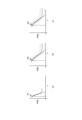
図2は、実施形態1にかかる試料1が有するパターン10の構成を模式的に示す図である。図2(a)~(c)はパターン10の平面図であり、図2(d)~(f)はパターン10の斜視図である。
FIG. 2 is a diagram schematically showing the structure of the
図2に示すように、パターン10が有するラインパターン11~13は、それぞれ複数のラインを備えるラインアンドスペース(LS)パターンである。複数のラインは、シリコンが有するダイアモンド構造の結晶方位である<111>方向と交わる方向に延びる。<111>方向と交わる方向とは、例えば<111>方向と直交する方向である。また例えば、<111>方向と交わる方向は、<111>方向と完全に直交していなくともよい。
As shown in FIG. 2,
より具体的には、ラインパターン11は、ラインパターン11~13のうち、<111>方向に直交する方向に最も近い方向に延伸している。ラインパターン12は、ラインパターン11に対して例えば時計回りに0.2°回転している。ラインパターン13は、ラインパターン11に対して例えば時計回りに0.4°回転している。
More specifically, the
複数のラインの上面11t~13tは、試料1の主面である(110)面から構成される。複数のラインの延伸方向の側面11s~13sは、少なくとも1つの{111}結晶面を有する。ラインパターン11は、<111>方向に略直交しており、その側面11sは略単一の1つの{111}結晶面から構成される。そして、ラインパターン11の側面11sの粗度、つまり、LER(Line Edge Roughness)は略ゼロである。
The
ラインパターン12は、<111>方向に直交する方向から若干回転している。この場合、ラインパターン12の側面12sには、結晶学的な周期を持って原子ステップ12aが現れる。
The
ここで、原子ステップとは、結晶表面上に現れる1原子~数原子で構成される原子層の段差のことである。原子ステップの大きさは結晶面によって決まっている。シリコンの{111}面の場合、1原子で構成される原子ステップは3.14Å(約0.3nm)である。原子ステップの周期は、すなわち原子ステップの間隔のことであり、ラインパターンの延伸方向と結晶方位とのずれ量によって異なる。ずれ量が大きいと原子ステップの間隔は狭くなり、ずれ量が小さいと原子ステップの間隔は広くなる。 Here, the atomic step is a step of an atomic layer composed of one to several atoms appearing on the crystal surface. The size of the atomic step is determined by the crystal plane. In the case of the {111} plane of silicon, the atomic step composed of one atom is 3.14 Å (approximately 0.3 nm). The period of atomic steps is the interval between atomic steps, and varies depending on the amount of deviation between the extending direction of the line pattern and the crystal orientation. If the shift amount is large, the atomic step interval will be narrow, and if the shift amount is small, the atomic step interval will be wide.
側面12sの周期的な原子ステップ12aによって、ラインパターン12は所定のLERを有する。例えば原子ステップ12aが1原子で構成されている場合には、ラインパターン12のLERは0.3nm、3σでは0.9nmである。
Due to the periodic
ラインパターン13は、<111>方向に直交する方向からラインパターン12よりも更に回転している。このため、ラインパターン13の側面13sには、ラインパターン12よりも短い周期で原子ステップ13aが現れる。ラインパターン13は、例えばラインパターン12と同じLERを有する。
The
(試料の製造方法)
次に、図3を用いて、実施形態1の試料1の製造方法について説明する。図3は、実施形態1にかかる試料1の製造方法の手順の一例を示す模式図である。
(Sample manufacturing method)
Next, a method for manufacturing
図3(a)に示すように、(110)面を主面とするシリコン製のウェハ1wに、条件出し用のラインLa~Leを形成する。ラインLa~Leは、アライメントマークMKsを基準にして、時計回りに例えば0.1°ずつ回転している。それぞれのラインLa~LeにもアライメントマークMKa~MKeが設けられる。
As shown in FIG. 3A, lines La to Le for setting conditions are formed on a
このようなラインLa~Le及びアライメントマークMKa~MKe,MKsは、例えば電子線描画等によりレジストパターンを形成し、このレジストパターンをマスクに、KOH溶液等のアルカリ性エッチング溶液で、ウェハ1wを所定深さまでウェットエッチングすることで得られる。 Such lines La to Le and alignment marks MKa to MKe and MKs are formed by forming a resist pattern by, for example, electron beam drawing. obtained by wet etching up to
KOH溶液等を用いたウェットエッチングでは、結晶面によってウェットエッチング速度が異なる。それぞれのラインLa~Leの側面にはウェットエッチング速度が最も遅い{111}結晶面が現れる。原子ステップは、ラインLa~Leの延伸方向が完璧な結晶面方位から若干ずれることで生じる。 In wet etching using a KOH solution or the like, the wet etching rate differs depending on the crystal plane. A {111} crystal plane having the slowest wet etching rate appears on the side surface of each of the lines La to Le. Atomic steps occur when the extending directions of the lines La to Le deviate slightly from the perfect crystal plane orientation.
このように得られたラインLa~Leのうち、どのラインLa~Leが<111>方向と直交する方向に最も近い延伸方向を有するかを確認する。つまり、原子ステップが生じていないもの、あるいは、ラインLa~Leのうち原子ステップが最も少ないものを選べばよい。ここでは、ラインLbがそれに該当するものとする。この場合、ラインLbと同じ回転角度となるようラインパターン11を形成する。
Among the lines La to Le thus obtained, it is confirmed which of the lines La to Le has the drawing direction closest to the direction perpendicular to the <111> direction. In other words, the line in which no atomic steps are generated or the line in which the atomic steps are the least among the lines La to Le should be selected. Here, the line Lb shall correspond to it. In this case, the
図3(b)に示すように、ラインパターン11を形成する際には、ラインLbに設けられたアライメントマークMKbと、基準となるアライメントマークMKsとに合わせてレジストパターンを形成し、ウェハ1wをウェットエッチングする。
As shown in FIG. 3B, when forming the
ラインパターン12を形成する際には、ラインLbから0.2°回転しているラインLdのアライメントマークMKdと、アライメントマークMKsとに合わせてレジストパターンを形成し、ウェハ1wをウェットエッチングする。
When forming the
ラインパターン13を形成する際には、ラインLdから更に0.2°回転しているラインのアライメントマークと、アライメントマークMKsとに合わせてレジストパターンを形成し、ウェハ1wをウェットエッチングする。
When forming the
これにより、各ラインパターン11~13の側面には{111}結晶面が現れる。また、<111>と直交する方向からの回転角度に応じて、側面に原子ステップが形成されていく。 As a result, {111} crystal planes appear on the side surfaces of the line patterns 11-13. Further, atomic steps are formed on the side surface according to the rotation angle from the direction orthogonal to <111>.
以上により、実施形態1の試料1が製造される。
As described above, the
(計測装置の構成例)
次に、図4及び図5を用いて、試料1を用いた較正が行われる計測装置200の構成例について説明する。図4は、実施形態1にかかる計測装置200の構成の一例を示す模式図である。計測装置200は、例えばパターンの寸法変換差やLER等を計測する測長SEMとして構成されている。
(Configuration example of measuring device)
Next, a configuration example of the
図4に示すように、計測装置200は、電子ビームEBの照射源としての電子銃221が設置された鏡筒211と、ウェハWが配置される試料室212と、計測装置200の各部を制御する制御部270と、を備える。
As shown in FIG. 4, the
鏡筒211は、閉塞された上端部と、電子ビームEBを通過させるために開放された下端部と、を備える筒状である。試料室212は、ウェハWを収容可能に構成される。鏡筒211と試料室212とは気密に封止された状態で組み合わされている。鏡筒211内および試料室212内は、図示しないポンプ等により減圧に保持することが可能なように構成される。
The
鏡筒211内には、上端部近傍から順に、電子銃221、集束レンズ231a,231b、コイル241a,241b,242a,242b、対物レンズ232、及び検出器251が設置される。
Inside the
電子銃221は、鏡筒211内下方に向かって電子ビームEBを照射する。電子銃221から照射された電子ビームEBは、鏡筒211の長軸方向に沿うように進行する。
The
集束レンズ231a,231bは、鏡筒211の光軸を中心として同心円状に巻かれた電磁コイルであって、磁界により電子ビームEBを集束させる。
The focusing
コイル241a,241b,242a,242bは、電子ビームEBを偏向させるため、または非点収差補正をするため、2つで1組になった電磁コイルであって、鏡筒211の光軸に対して互いに対称に配置される。
The
対物レンズ232は、鏡筒211の光軸を中心として同心円状に巻かれた電磁コイルであって、磁界によりウェハWへ向かって出射した電子ビームEBを集束させる。
The
検出器251は、電子ビームEBが入射されたウェハWから発生した二次電子を検出する。
The
試料室212内には、ウェハWが載置されるウェハステージ261が設置されている。ウェハステージ261にはアクチュエータ262が取り付けられ、ウェハステージ261を前後左右に駆動可能に構成される。ウェハステージ261が駆動することで、ウェハW上の所定のポイントに電子ビームEBを照射して、ウェハWに入射させることができる。
A
制御部270は、CPU(Central Processing Unit)、RAM(Random Access Memory)、記憶装置、及びI/Oポート等を備えたコンピュータとして構成されている。
The
図5は、実施形態1にかかる計測装置200の制御部270が備えるハードウェア構成の一例を示すブロック図である。
FIG. 5 is a block diagram showing an example of a hardware configuration included in the
図1に示すように、計測装置200の制御部270は、CPU201、記憶装置としてのROM(Read Only Memory)202、RAM203、表示部204、入力部205、及びIOポート206を有している。制御部270では、これらのCPU201、ROM202、RAM203、表示部204、入力部205、及びIOポート206がバスラインを介して接続されている。
As shown in FIG. 1 , the
CPU201は、各種制御プログラムを用いて計測装置200により計測を行う。また、CPU201は、コンピュータプログラムである較正プログラム207を用いて計測装置200の較正を行う。較正プログラム207は、コンピュータで実行可能な、較正を行うための複数の命令を含むコンピュータ読取り可能な記録媒体を有するコンピュータプログラムプロダクトである。較正プログラム207では、これらの複数の命令が、計測装置200の較正処理をコンピュータに実行させる。
The
表示部204は、液晶モニタなどの表示装置であり、CPU201からの指示に基づいて、計測装置200による計測結果や較正パラメータなどを表示する。入力部205は、マウスやキーボードを備えて構成され、使用者から外部入力される計測や較正に必要なパラメータ等の指示情報を入力する。入力部205へ入力された指示情報は、CPU201へ送られる。
A
IOポート206は、電子銃221、集束レンズ231a,231b、コイル241a,241b,242a,242b、対物レンズ232、検出器251、及びウェハステージ261のアクチュエータ262等に接続されている。
The
CPU201は、ROM202等から読み出した制御プログラムの内容に沿うように、IOポート206を介して、電子銃221、集束レンズ231a,231b、コイル241a,241b,242a,242b、対物レンズ232、検出器251、及びウェハステージ261のアクチュエータ262等を制御する。
The
較正プログラム207は、較正パラメータ等と共にROM202内に格納されており、バスラインを介してRAM203へロードされる。図5では、較正プログラム207がRAM203へロードされた状態を示している。
A
CPU201はRAM203内にロードされた較正プログラム207を実行する。具体的には、制御部270では、使用者による入力部205からの指示入力に従って、CPU201がROM202内から較正プログラム207を読み出してRAM203内のプログラム格納領域に展開して各種較正処理を実行する。CPU201は、この各種較正処理に際して生じる各種データをRAM203内に形成されるデータ格納領域に一時的に記憶させておく。較正処理が終了すると較正パラメータは更新される。
制御部270で実行される較正プログラム207はモジュール構成となっており、これらが主記憶装置上にロードされ、主記憶装置上に生成される。
The
(計測装置の較正方法)
次に、図6~図9を用いて、実施形態1の試料1を用いて実施される計測装置200の較正方法について説明する。
(Method for calibrating measuring device)
Next, a method for calibrating the
計測装置200の較正は、例えばパターンのLER及び自己相関長(Correlation Length)ξに対して行われる。自己相関長ξは、同じ周期構造がどれくらいの間隔で繰り返されるかの指標である。試料1が有するパターン10のLERに関して言えば、自己相関長ξは原子ステップが現れる間隔に相当する。試料1と異なり、ランダムなLERを有する実パターンの計測において、LERの値そのものに加え、自己相関長ξは重要なパラメータの1つであり、これを正確に較正することも非常に重要である。
Calibration of
試料1は、所定の結晶面と、その結晶面に現れる原子ステップを利用した既知のLER及び自己相関長ξを有する較正用試料である。また、試料1の有するLERは非常に小さい。このような試料1を用いることで、計測装置200を精度よく較正することができる。
A
図6は、実施形態1にかかる試料1のパターン10が示すLERのパワースペクトル密度関数(PSD:Power Spectral Density Function)を模式的に示すグラフである。PSDは、連続信号が周波数帯域ごとに持つパワー分布を表す。
FIG. 6 is a graph schematically showing the LER power spectral density function (PSD) indicated by the
図6のグラフの横軸は周波数(f)であり、縦軸はPSDである。また、グラフの実線は計測装置200によるパターン10の実測値であり、破線は実測値の正確度の許容範囲を示す。また、グラフの一点鎖線は、計測装置200で得られる画像のノイズ成分を除去した値をプロットしたものである。
The horizontal axis of the graph in FIG. 6 is frequency (f), and the vertical axis is PSD. Also, the solid line in the graph is the measured value of the
パターン10が有するLERの自己相関長ξは、例えばグラフの低周波の平坦領域の値から1/e下がったポイントP1~P3における周波数の逆数として求めることができる。ここで、「e」は自然対数の底である。
The LER autocorrelation length ξ of the
図6(a)に示すように、LERがゼロと見做せ、自己相関長ξが無限大となるラインパターン11のPSDは、理想的にはデルタ関数となる。ただし、計測装置200の画像に起因するノイズ成分が現れるため、実線で示す値が実測値として得られる。グラフのポイントP1から求められる自己相関長ξも無限大とはならない。
As shown in FIG. 6(a), the PSD of the
図6(b)に示すように、所定周期の原子ステップを有するラインパターン12のPSDは、ラインパターン11のPSDよりも緩やかな傾きを示し、ポイントP2から求められる自己相関長ξはラインパターン11よりも小さくなる。
As shown in FIG. 6B, the PSD of the
図6(c)に示すように、更に小さな周期の原子ステップを有するラインパターン13のPSDは、ラインパターン12のPSDよりも緩やかな傾きを示し、ポイントP3から求められる自己相関長ξはラインパターン12よりも小さくなる。
As shown in FIG. 6(c), the PSD of the
図7は、実施形態1にかかる試料1および任意のサンプルのラインパターン11~13,A~Cが示すLER及び自己相関長ξの実測値の一例を示すグラフである。
FIG. 7 is a graph showing an example of measured values of the LER and the autocorrelation length ξ indicated by the
図7(a)はラインパターン11~13のLERのグラフであり、実線が実測値を示し、破線が実測値の正確度の許容範囲を示す。グラフの横軸は各ラインパターン11~13を示し、グラフの縦軸はLERである。図7(b)はラインパターン11~13自己相関長ξのグラフであり、実線が実測値を示し、破線が実測値の正確度の許容範囲を示す。グラフの横軸は各ラインパターン11~13を示し、グラフの縦軸は自己相関長ξである。図7(c)は任意のサンプルのラインパターンA~CのLERのグラフであり、実線が実測値を示し、破線が実測値の正確度の許容範囲を示す。グラフの横軸は各ラインパターンA~Cを示し、グラフの縦軸はLERである。
FIG. 7(a) is a graph of LER for
図7(a)(b)の例では、ラインパターン12,13のLER及び自己相関長ξの実測値は許容範囲内に入っている。しかし、ラインパターン11のLER及び自己相関長ξの実測値は共に許容範囲から外れている。つまり図7(a)(b)の例では、計測装置200は、LERが無限小、つまり略ゼロの場合の計測値の補正が必要であることが判る。
In the examples of FIGS. 7A and 7B, the measured values of the LER and the autocorrelation length ξ of the
このような状態で、任意のサンプルである実サンプルのラインパターンA~CのLERを計測すると、図7(c)に示すように、やはり、LERが小さい側のラインパターンAの実測値が許容範囲からはずれてしまう。 In this state, when the LER of line patterns A to C of real samples, which are arbitrary samples, is measured, as shown in FIG. It goes out of range.
図8は、実施形態1にかかる試料1および任意のサンプルのラインパターン11~13,A~Cが示すLER及び自己相関長ξの較正後の実測値の一例を示すグラフである。
FIG. 8 is a graph showing an example of measured values after calibration of the LER and the autocorrelation length ξ indicated by the
図8(a)ラインパターン11~13LERのグラフであり、実線が計測装置200の較正後の実測値を示し、破線が実測値の正確度の許容範囲を示す。グラフの横軸は各ラインパターン11~13を示し、グラフの縦軸はLERである。図8(b)はラインパターン11~13自己相関長ξのグラフであり、実線が計測装置200の較正後の実測値を示し、破線が実測値の正確度の許容範囲を示す。グラフの横軸は各ラインパターン11~13を示し、グラフの縦軸は自己相関長ξである。図8(c)は任意のサンプルのラインパターンA~CのLERのグラフであり、実線が実測値を示し、破線が実測値の正確度の許容範囲を示す。グラフの横軸は各ラインパターンA~Cを示し、グラフの縦軸はLERである。
FIG. 8(a) is a graph of
図8(a)(b)に示すように、ラインパターン11~13の全てのプロットが許容範囲内に入っている。既知のLER及び自己相関長ξを有する試料1を用いた較正により、計測装置200において、図8(c)に示すように、その後の未知でランダムなLER及び自己相関長ξを有するサンプルの精度の高い計測が可能となる。
As shown in FIGS. 8(a) and 8(b), all plots of line patterns 11-13 are within the allowable range. By
なお、図7では、LERが小さくなり、また、自己相関長ξが大きくなるほど計測装置200による実測値がずれていく例について示したが、試料1で特定できる計測装置の実測値のずれの傾向はこれに限られない。計測装置によっては、LERが大きくなり、または、自己相関長ξが小さくなるほど実測値がずれる場合や、特定のLER及び自己相関長ξにおいて実測値がずれる場合等があり、試料1を用いればこれらの傾向を把握することができる。
FIG. 7 shows an example in which the values measured by the measuring
図9は、実施形態1にかかる試料1を用いた計測装置200の較正方法の手順の一例を示すフロー図である。
FIG. 9 is a flow diagram showing an example of a procedure of a method for calibrating the measuring
図9に示すように、計測装置200により、試料1の各ラインパターン11~13を計測し、LER及び自己相関長ξの実測値を取得する(ステップS101)。
As shown in FIG. 9, the
得られた実測値の正確度が許容範囲内か否かを判定する(ステップS102)。 It is determined whether or not the accuracy of the obtained measured value is within the allowable range (step S102).
実測値の正確度が許容範囲内でない場合には(ステップS102:No)、計測装置200の較正を行う(ステップS103)。
If the accuracy of the measured value is not within the allowable range (step S102: No), the measuring
計測装置200の較正後、改めて、試料1の各ラインパターン11~13を計測し、LER及び自己相関長ξの実測値を取得する(ステップS104)。
After calibrating the
得られた実測値の正確度が許容範囲内か否かを判定する(ステップS102)。実測値の正確度が許容範囲内である場合には(ステップS102:Yes)、処理を終了する。 It is determined whether or not the accuracy of the obtained measured value is within the allowable range (step S102). If the accuracy of the measured values is within the allowable range (step S102: Yes), the process is terminated.
以上により、実施形態1の試料1を用いた計測装置200の較正が終了する。
As described above, the calibration of the measuring
(比較例)
測長SEM等の計測装置で計測されたLERはノイズの影響で大きく見積もられる傾向にある。そこで、比較例の構成として、計測装置の較正によりノイズ成分をソフトウェア上で差し引く計算手法が提案されている。
(Comparative example)
The LER measured by a measurement device such as a critical dimension SEM tends to be overestimated due to the influence of noise. Therefore, as a configuration of a comparative example, a calculation method is proposed in which noise components are subtracted on software by calibrating a measuring device.
しかしながら、計算方法が定まっておらず、同じサンプルを用いて計測したLER及び自己相関長ξの値が異なってしまう。また、既知のLER及び自己相関長ξを有する標準試料が存在せず、得られたLER及び自己相関長ξの正確度を検証することができないという種々の課題がある。標準試料に関して言えば、将来的に求められる2nm以下のLER計測を可能とするような試料が必要となってくると考えられる。 However, the calculation method is not fixed, and the values of LER and autocorrelation length ξ measured using the same sample are different. In addition, there are various problems in that there is no standard sample with known LER and autocorrelation length ξ, and the accuracy of the obtained LER and autocorrelation length ξ cannot be verified. As for the standard sample, it is considered that a sample that enables LER measurement of 2 nm or less, which is required in the future, will be required.
しかしながら、光リソグラフィや電子線リソグラフィを用いた微細加工では、2nm以下のLERを有する標準試料を意図的に作製することは非常に困難である。 However, in microfabrication using optical lithography or electron beam lithography, it is very difficult to intentionally prepare a standard sample having an LER of 2 nm or less.
実施形態1の試料1によれば、<111>方向に交わる方向に延び、延伸方向の側面が少なくとも1つの{111}結晶面を有するラインパターン11~13を備える。これにより、既知のLER及び自己相関長ξを有する試料1が得られる。原子ステップに起因するLERは非常に微小であるので、試料1は例えば1nm前後のLERに基づき、計測装置200を較正することが可能となる。
According to the
実施形態1の試料1によれば、試料1は種々の大きさのウェハWにはめ込まれて用いられる。これにより、様々な計測装置200に共通して試料1を用いることができる。よって、様々な計測装置200のいずれにおいても、同じサンプルに対して同一の計測結果が得られるよう、これらの計測装置200を較正することができる。
According to the
なお、実施形態1の試料1は、チップ状であり、ウェハWにはめ込まれて用いられることとしたが、これに限られない。ウェハ1wにパターン10を形成した後、チップに切り出すことなく、そのまま計測装置200での計測および較正に用いられてもよい。
Note that the
また、上述のように原子ステップは1原子~数原子で構成することが可能であり、原子ステップを構成する原子数を調整することで、種々のLERに対応することができる。上述のように、原子ステップの構成原子が1原子である場合には、LERは0.3nm(3σで0.9nm)である。原子ステップの構成原子が2原子である場合には、原子ステップの段差は6.28Åであり、LERは0.6nm(3σで1.8nm)となる。 Further, as described above, the atomic step can be composed of one to several atoms, and by adjusting the number of atoms constituting the atomic step, it is possible to deal with various LERs. As described above, when the atomic step consists of one atom, the LER is 0.3 nm (0.9 nm at 3σ). When the atomic step consists of two atoms, the step height of the atomic step is 6.28 Å and the LER is 0.6 nm (1.8 nm at 3σ).
原子ステップの構成原子数は、ラインパターンの回転角度を大きくすることで増加させることができる。つまり、<111>方向の直交方向からのずれが大きくなるほど、段差の大きな原子ステップが現れやすい。これにより、原子ステップの間隔、つまり、自己相関長ξも縮小方向に調整することができる。 The number of constituent atoms of the atomic step can be increased by increasing the rotation angle of the line pattern. In other words, the larger the deviation from the orthogonal direction to the <111> direction, the more likely atomic steps with large steps appear. As a result, the interval between atomic steps, that is, the autocorrelation length ξ can also be adjusted in the contraction direction.
原子ステップの段差や間隔は、エッチング液やウェットエッチングの条件等によってもコントロールすることが可能である。 The steps and intervals of the atomic steps can also be controlled by the etchant, wet etching conditions, and the like.
また、試料の材料となる(110)面を主面とするウェハは、シリコンだけでなく、GaAsまたはGaSn等の閃亜鉛(Zincblende)構造結晶の多元結晶を有するウェハであってもよい。例えば、GaAsの場合、格子間隔がシリコンとは若干異なり、GaAsの{111}結晶面の面間隔は3.26Åと、シリコンより若干大きい。このように、ウェハの材料を様々に選定することによっても、LERの大きさを制御することができる。 Moreover, the wafer having the (110) plane as the main surface, which is the material of the sample, may be a wafer having a multi-element crystal of a zinc blende structure crystal such as GaAs or GaSn, as well as silicon. For example, in the case of GaAs, the lattice spacing is slightly different from that of silicon. Thus, the magnitude of the LER can also be controlled by variously selecting the wafer material.
(変形例1)
次に、図10を用いて、実施形態1の変形例1の試料2について説明する。図10は、実施形態1の変形例1にかかる試料2が有するパターン20の構成を模式的に示す平面図である。変形例1の試料2はLERの周期がランダムである点が、上述の実施形態1の試料1とは異なる。
(Modification 1)
Next, Sample 2 of
図10に示すように、試料2の(110)面である主面にはパターン20が配置されている。パターン20は、第1のラインパターンとしてのラインパターン21、第2のラインパターンとしてのラインパターン22、及び第3のラインパターンとしてのラインパターン23を含む。
As shown in FIG. 10, a pattern 20 is arranged on the main surface of the sample 2, which is the (110) plane. The pattern 20 includes a
ラインパターン21~23は、<111>方向に略直交する方向に延伸している。つまり、ラインパターン21~23のベースとなるパターンは、上述の実施形態1のラインパターン11と同様に構成されており、LERが略ゼロであり、自己相関長ξは原理的には無限大である。
The
このようなラインパターンをベースとして、ラインパターン22,23にはランダムな周期を有するLERが導入されている。このようなラインパターン22,23は、例えばアッシングまたはドライエッチング等により、ラインパターン22,23の側面を荒らして微小な凹凸22c,23cを設けることで形成することができる。
Based on such line patterns, LERs having random periods are introduced into the
また、ラインパターン23は、ラインパターン22よりも大きなLERを有する。LERは、アッシングやドライエッチングの条件を異ならせることで調整することができる。例えば、アッシングであれば、プラズマ生成用電圧を高めたり、処理時間を長くしたりすることで、より大きなLERが得られる。ドライエッチングであれば、上記手法の他、所定のLERを有するレジストパターンをマスクに、選択的にエッチングを行うことで異なるLERが得られる。
ラインパターン22,23のLER及び自己相関長ξを既知のものとするには、例えば、予め、使用するアッシングやドライエッチンの条件ごとに、これらの条件により作成されたダミーパターン等を、透過型電子顕微鏡(TEM:Transmission Electron Microscope)等により観測し、LER及び自己相関長ξの値を取得しておけばよい。
In order to make the LER and the autocorrelation length ξ of the
なお、ラインパターン21には、アッシングやドライエッチング等は行わず、初期状態のままのミラー面とする。
The
(変形例2)
次に、図11を用いて、実施形態1の変形例2の試料3について説明する。図11は、実施形態1の変形例2にかかる試料3が有するパターン30の構成を模式的に示す平面図である。変形例2の試料3はLERの導入手法が、上述の変形例1の試料2とは異なる。
(Modification 2)
Next,
図11に示すように、試料3の(110)面である主面にはパターン30が配置されている。パターン30は、第1のラインパターンとしてのラインパターン31、第2のラインパターンとしてのラインパターン32、及び第3のラインパターンとしてのラインパターン33を含む。
As shown in FIG. 11, a
ラインパターン31~33は、<111>方向に略直交する方向に延伸している。つまり、ラインパターン31~33のベースとなるパターンは、上述の実施形態1のラインパターン11と同様に構成されており、LERが略ゼロであり、自己相関長ξは原理的には無限大である。
The
このようなラインパターンをベースとして、ラインパターン32,33には、パーティクル32p,33pを利用して、ランダムな周期を有するLERが導入されている。つまり、粒子サイズが既知のパーティクル32p,33pをそれぞれのラインパターン32,33に付着させる。ラインパターン33に付着させるパーティクル33pは、ラインパターン32に付着させるパーティクル32pよりも粒子サイズの大きなものとする。
Based on such line patterns, LER having a random period is introduced into
なお、ラインパターン31には、パーティクルを付着させることなく、初期状態のままのミラー面とする。
Note that the
[実施形態2]
以下、図面を参照して、実施形態2について詳細に説明する。実施形態2では、試料の材料となる基板としてSOI(Silicon On Insulator)ウェハを用いる点が、上述の実施形態1の構成とは異なる。
[Embodiment 2]
The second embodiment will be described in detail below with reference to the drawings. Embodiment 2 differs from the configuration of
図12は、或るラインパターン40が有する各種結晶面を示す模式図である。ラインパターン40は、(110)面を主面とする基板に<111>方向と略直交する方向に延びるラインを有する。
FIG. 12 is a schematic diagram showing various crystal planes of a
図12に示すように、ラインパターン40は、(110)面である上面41に対して略垂直な{111}結晶面である側面42と、(110)面である底面43との接合部分に裾部44を有する。裾部44は、ラインパターン40の形成時に出現した他の{111}結晶面である(参考文献:Micro and Nano Engineering3(2019)44-49)。裾部44の{111}結晶面は、側面42の{111}結晶面とは異なる角度を有している。
As shown in FIG. 12, the
例えば計測装置200等による計測時、顕微鏡の焦点深度が深い場合等において、上記の裾部44のような斜めの{111}結晶面が画像に写り込み、ラインパターン40の輪郭が不鮮明になる場合がある。
For example, when measuring with the measuring
以下に述べる実施形態2の構成は、斜めの{111}結晶面が形成されてしまうのを抑制する。 The configuration of Embodiment 2 described below suppresses the oblique {111} crystal planes from being formed.
(試料の製造方法)
図13は、実施形態2にかかる試料の材料となるSOIウェハ5wと、試料が有するラインパターン51とを模式的に示す断面図である。
(Sample manufacturing method)
FIG. 13 is a cross-sectional view schematically showing an
図13(a)に示すように、SOIウェハ5wは、シリコン等から構成される基板50sb、シリコン酸化層等の絶縁層から構成されるボックス層50bx、及びシリコン層等から構成される活性層50acを備える。
As shown in FIG. 13A, the
活性層50acは、(110)面を主面とする結晶構造を有する。SOIウェハ5wが、例えばSIMOX(Separation by IMplantation of OXygen)方式で作製されている場合には、基板50sbも(110)結晶となる。基板50sbが(110)結晶であると、劈開等の加工が容易であるなどの利点がある。
The active layer 50ac has a crystal structure with the (110) plane as the main surface. If the
ただし、基板50sbは必ずしも(110)結晶構造を有する必要はない。例えば、SOIウェハを貼り合わせ方式で作製した場合には、基板が(110)結晶以外の結晶構造を有することもある。 However, the substrate 50sb does not necessarily have a (110) crystal structure. For example, when an SOI wafer is produced by a bonding method, the substrate may have a crystal structure other than the (110) crystal.
SOIウェハ5wを用いて、SOIウェハ5wの活性層50acにラインを形成することで、ラインパターン51を得ることができる。
A
図13(b)に示すように、第1のラインパターンとしてのラインパターン51は、底面51bがボックス層50bxに達するラインアンドスペースパターンとなっている。ラインパターン51は、例えば活性層50acの結晶方位である<110>方向に略直交する方向に延びる。
As shown in FIG. 13B, the
KOH溶液等によるウェットエッチングでは、シリコン等である活性層50acに対し、シリコン酸化層等であるボックス層50bxは殆どエッチングされず、高い選択比を有する。この高選択比を利用して、図12に示した裾部44の{111}結晶面のような傾斜面が消失するまでウェットエッチングを継続することにより、傾斜面の無いラインパターン51が得られる。
In wet etching with a KOH solution or the like, the box layer 50bx, which is a silicon oxide layer or the like, is hardly etched with respect to the active layer 50ac, which is silicon or the like, and has a high selection ratio. Utilizing this high selectivity, wet etching is continued until the inclined plane such as the {111} crystal plane of the
このようなSOIウェハ5wを用いた試料に対しては、上述の実施形態1及びその変形例1,2の構成を適用することが可能である。つまり、ラインパターン51をベースに、<110>方向の直交方向から意図的にずらして延伸させた第2及び第3のラインパターンを形成することで、上述の実施形態1に相当する試料が得られる。また、ラインパターン51をベースに、ドライエッチング等により側面を荒らした第2及び第3のラインパターンを形成することで、上述の実施形態1の変形例1に相当する試料が得られる。また、ラインパターン51をベースに、粒子サイズが既知であるパーティクルを付着させた第2及び第3のラインパターンを形成することで、上述の実施形態1の変形例2に相当する試料が得られる。
The configurations of
なお、SOIウェハの作製条件や、作製後の研磨処理等により、活性層の厚さは種々に調整可能である。厚膜の活性層を有するSOIウェハを使って、ドライエッチングとウェットエッチングとの複合処理によりラインパターンを形成してもよい。 Note that the thickness of the active layer can be variously adjusted depending on the manufacturing conditions of the SOI wafer, the polishing treatment after manufacturing, and the like. A line pattern may be formed by a combination of dry etching and wet etching using an SOI wafer having a thick active layer.
ドライエッチングは垂直性の高い深溝の形成に優れる。ただし、ドライエッチングによる加工面に完全な結晶面が現れるわけではない。一方、KOH溶液等を用いたウェットエッチングでは、加工面は略完全な結晶面となるが、ウェットエッチングは等方的にエッチングが進行することから狭ピッチのパターン形成には不向きである。 Dry etching is excellent in forming deep grooves with high verticality. However, a complete crystal plane does not appear on the surface processed by dry etching. On the other hand, in wet etching using a KOH solution or the like, the processed surface becomes a substantially perfect crystal plane, but wet etching progresses isotropically and is therefore unsuitable for narrow-pitch pattern formation.
そこで、ドライエッチングにより厚膜の活性層をボックス層に達するまで深掘りし、その後、KOH溶液等を用いたウェットエッチングを行うことで、ウェットエッチングの処理時間を短縮することができ、ラインパターンのピッチが広がってしまうことを抑制できる。これにより、側面に{111}結晶面を有する狭ピッチのラインパターンを形成することができる。 Therefore, dry etching is performed to deepen the thick active layer until it reaches the box layer, and then wet etching is performed using a KOH solution or the like. It is possible to suppress the spread of the pitch. As a result, a narrow-pitch line pattern having {111} crystal planes on the side surfaces can be formed.
狭ピッチのラインパターンを形成する際、金属触媒エッチング(MacEtch:Metal-Assisted Chemical Etching)等の、より高アスペクト比のパターンの加工性に優れる手法を用いてもよい。 When forming a narrow-pitch line pattern, a method such as metal-assisted chemical etching (MacEtch), which is excellent in workability of a pattern with a higher aspect ratio, may be used.
(変形例1)
次に、図14及び図15を用いて、実施形態2の変形例1の試料6について説明する。変形例1の試料6は、電気的な状態の異なるラインパターン61a~63a,61f~63fを備える点が、上述の実施形態2とは異なる。
(Modification 1)
Next, the
図14は、実施形態2の変形例1にかかる試料6の構成の一例を模式的に示す平面図である。図14に示すように、変形例1の試料6もSOIウェハから構成され、ボックス層60bx上に配置されたパターン60を備える。パターン60は、ラインパターン61a~63a,61f~63fを含む。
FIG. 14 is a plan view schematically showing an example of the configuration of the
第1のラインパターンとしてのラインパターン61a,61fは、<110>方向と略直交する方向に延び、実質的にゼロと見做せるLER、及び実質的に無限大の自己相関長ξを有する。第2のラインパターンとしてのラインパターン62a,62f、及び第3のラインパターンとしてのラインパターン63a,63fには、上述の実施形態1及びその変形例1,2の少なくともいずれかの手法により、所定の自己相関長ξを有するLERが導入されている。
The
また、ラインパターン61f~63fは、絶縁層であるボックス層60bx上に配置されていることからフローティング状態となっている。ラインパターン61a~63aは、接地線64に接続されてアース状態となっている。これにより、計測装置の電子ビームによる帯電が計測制度に与える影響を調べることができる。
Further, the
ただし、ラインパターン61a~63aは、これ以外の手法でアース状態とされていてもよい。例えば、SOIウェハの基板と物理的に接触させることで、ラインパターン61a~63aをアース状態にすることができる。また、ラインパターン61a~63aの体積が充分に大きければ電気的な容量も大きくなり、帯電の影響を無視することができる。
However, the
図15は、実施形態2の変形例1にかかるラインパターン61a,61fから得られる画像の信号強度プロファイルを示すグラフである。グラフの横軸は、ラインパターン61a,61fの延伸方向と直交する方向の断面における計測位置であり、グラフの縦軸は信号強度である。
FIG. 15 is a graph showing signal intensity profiles of images obtained from the
図15に示すように、フローティング状態で帯電されたラインパターン61fの線幅は、アース状態のラインパターン61aの線幅よりも太く計測される(参考文献:Journal of Vacuum Science&Technology B36,06J502(2018))。帯電されていない状態でラインパターン61a,61fを計測すると、これらの信号強度プロファイルはほぼ一致し、これらが等しい線幅であることが判っている。したがって、図15のグラフの信号強度プロファイルの違いは帯電の影響によるものであることが判る。
As shown in FIG. 15, the line width of the
実施形態2の変形例1の試料6によれば、帯電の影響下にあるパターンの計測結果の確度および精度を知ることができ、計測装置における帯電対策技術の評価も可能となる。
According to the
(変形例2)
上述の実施形態2及びその変形例1の構成を欠陥検査装置の較正用の試料に転用することも可能である。計測装置としての欠陥検査装置は、例えば隣り合うダイ同士のパターンを比較することにより、ピンドット欠陥やピンホール欠陥等の欠陥を検出する装置である。
(Modification 2)
It is also possible to divert the configurations of the second embodiment and its first modified example described above to a sample for calibration of a defect inspection apparatus. A defect inspection device as a measurement device is a device that detects defects such as pin dot defects and pinhole defects by comparing patterns of adjacent dies, for example.
欠陥検査装置においては、欠陥検査装置の検出対象となるピンドット欠陥やピンホール欠陥等のサイズを意図的に変化させたプログラム欠陥と呼ばれる欠陥を導入したパターンを評価することで、所定サイズの欠陥を正しく検出できるか否かを判定することがある。判定結果は欠陥検査装置の較正に用いられる。 In the defect inspection system, defects of a predetermined size are detected by evaluating a pattern that introduces a defect called a program defect, which intentionally changes the size of a pin dot defect, a pinhole defect, etc. can be detected correctly. The judgment result is used for calibrating the defect inspection device.
しかしながら、判定に用いるパターンが所定の大きさ以上のLERを有していると、欠陥検査装置における評価を攪乱させる要因となってしまう。 However, if the pattern used for determination has an LER greater than or equal to a predetermined size, it becomes a factor that disturbs the evaluation in the defect inspection apparatus.
そこで、図16に示すように、実施形態2のラインパターン51をベースに、プログラム欠陥の無いラインパターン61ieと、プログラム欠陥65pを導入したラインパターン65ieとを形成することで、攪乱要因となるLERが実質的にゼロであるような状態で、欠陥検査装置の評価を行うことができる。また、プログラム欠陥65pの導入に際しては、LERの影響を考慮しなくともよく、プログラム欠陥65pを例えば約2nm以下の微小サイズとすることも可能である。
Therefore, as shown in FIG. 16, based on the
また、上述の変形例1のラインパターン61a,61fをベースに、プログラム欠陥の無いラインパターンと、プログラム欠陥を導入したラインパターンとを形成することで、帯電の影響が欠陥検査装置に与える影響をも調べることが可能となる。
Further, by forming a line pattern without programming defects and a line pattern with programming defects based on the
[実施形態3]
以下、図面を参照して、実施形態3について詳細に説明する。実施形態3の構成では、結晶成長により所定の結晶面を側壁に有するラインパターンを形成する点が、上述の実施形態1,2とは異なる。
[Embodiment 3]
The third embodiment will be described in detail below with reference to the drawings. The configuration of
(試料の製造方法)
図17は、実施形態3にかかるラインパターン71の形成方法の手順の一例を示す平面図である。
(Sample manufacturing method)
FIG. 17 is a plan view showing an example of the procedure of the method for forming the
図17(a)は、光リソグラフィや電子線リソグラフィ等のリソグラフィ技術と、反応性イオンエッチング(RIE:Reactive Ion Etching)等のドライエッチング技術とによって形成したラインパターン71pである。ラインパターン71pは、<110>方向と略直交する方向に延びる。
FIG. 17A shows a
図17(a)に示すように、リソグラフィとドライエッチングにより形成されたラインパターン71pは、例えばレジストパターンが有していたLERが転写されたり、ドライエッチングにより側壁荒れが起きたりすることによって側面に凹凸71cが形成されて、ラインパターン71pのLERが大きくなることがある。
As shown in FIG. 17(a), the
次に、ラインパターン71pの上面に絶縁層等による保護層(不図示)を形成する。ラインパターン71pの形成時、レジストパターン等の補助のためにハードマスクを形成しておき、それを保護層として転用してもよい。
Next, a protective layer (not shown) made of an insulating layer or the like is formed on the upper surface of the
次に、液相成長技術等を用いてラインパターン71pに対して結晶成長を行う。液相成長技術では、平衡状態に近い状態で結晶成長が進行するため、最安定面である{111}結晶面が容易に形成される。ラインパターン71p上面は保護層の存在により、結晶成長は殆ど行われない。
Next, crystal growth is performed on the
また、溶液または融液の温度を調整することで、溶解または融解等のエッチングと、結晶成長との両方が並行して行われる。これにより、ラインパターン71pの線幅の太りを抑制しつつ、主にラインパターン71p側面での結晶成長を行うことができる。
Also, by adjusting the temperature of the solution or melt, both etching such as dissolution or melting and crystal growth are performed in parallel. As a result, crystal growth can be performed mainly on the side surfaces of the
具体的には、溶液または融液の温度を平衡温度よりも若干高くすることで、まずはエッチングを進行させる。その際、ラインパターン71p側面の凹凸71cのような曲率半径が小さい部分が優先的にエッチングされる。その後、線幅が細りすぎないよう、溶液または融液の温度を下げて結晶成長を進行させる。
Specifically, etching proceeds by raising the temperature of the solution or melt slightly higher than the equilibrium temperature. At that time, portions with a small radius of curvature such as the
ラインパターン71pの側面が略完全な{111}結晶面で覆われたところで、液相成長を終了する。その後、ラインパターン71pの上面から図示しない保護層を除去する。
Liquid phase growth ends when the side surfaces of the
図17(b)は、以上により得られた第1のラインパターンとしてのラインパターン71である。ラインパターン71は、{111}結晶面である側面71sを有し、実質的にゼロと見做せるLER、及び実質的に無限大の自己相関長ξを有する。
FIG. 17B shows the
ラインパターン71をベースに、上述の実施形態1及びその変形例1,2の少なくともいずれかの手法により、所定の自己相関長ξを有するLERが導入された第2及び第3のラインパターンを形成することで、実施形態3の試料が得られる。
Based on the
なお、リソグラフィ技術とドライエッチング技術とを用いた加工においては、例えばハーフピッチが20nm以下の微細パターンを作製することも可能である。それには、例えば電子線リソグラフィ技術やダブルパターニング技術を用いればよい。ダブルパターニング技術は、二重露光により、1回の露光で形成したレジストパターンの間に、もう1回の露光で新たなレジストパターンを形成する技術である。 In processing using lithography technology and dry etching technology, it is also possible to fabricate a fine pattern with a half pitch of 20 nm or less, for example. For that purpose, for example, an electron beam lithography technique or a double patterning technique may be used. The double patterning technique is a technique of forming a new resist pattern by another exposure between the resist patterns formed by one exposure by double exposure.
実施形態3の試料によれば、例えばハーフピッチが20nm以下の微細なラインパターン71における計測結果の確度および精度を知ることができる。これを計測装置の較正に活かすことで、微細パターンにおける計測の精度を向上させることができる。
According to the sample of
なお、実施形態3の試料の材料としては、シリコンウェハ及びSOIウェハのいずれも用いることができる。 As the material of the sample of the third embodiment, both a silicon wafer and an SOI wafer can be used.
(変形例)
実施形態3における液相成長技術に替えて、変形例として、分子線エピタキシ(MBE:Molecular Beam Epitaxy)技術や有機金属気相成長(MOCVD:Metal Organic Chemical Vapor Deposition)技術等の気相成長技術を用いることも可能である。
(Modification)
Instead of the liquid phase epitaxy technique in
気相成長技術では、結晶成長の速度が液相成長技術に比べて遅く、線幅の制御が容易である。また、結晶成長の条件によって最安定面である{111}結晶面のみならず、{110}結晶面や{100}結晶面のような準安定面も形成可能である。得られる結晶面は、結晶成長の下地の結晶方位にも大きく依存する。これを利用して、例えば、ドライエッチング後にラインパターンの上面である(110)面を露出させておくことで、上面には(110)面が成長しやすく、側面には{111}結晶面が成長しやすい状態を作ることができる。 In the vapor phase epitaxy, the crystal growth rate is slower than in the liquid phase epitaxy, and the line width can be easily controlled. Further, depending on the crystal growth conditions, not only the {111} crystal plane, which is the most stable plane, but also metastable planes such as the {110} crystal plane and the {100} crystal plane can be formed. The obtained crystal plane greatly depends on the crystal orientation of the base for crystal growth. Using this, for example, by exposing the (110) plane, which is the upper surface of the line pattern after dry etching, the (110) plane easily grows on the upper surface and the {111} crystal plane is formed on the side surface. You can create conditions for growth.
なお、気相成長技術を用いる場合には、予め、ドライエッチング後のラインパターンの線幅を狭くしておくことが好ましい。電子線リソグラフィや極端紫外線(EUV:Extreme Ultraviolet)を用いたリソグラフィでは、ネガレジストが多用される。この場合、スペース幅に比べてライン幅(線幅)を狭くすることが容易である。これにより、気相成長により線幅が太っても所望の線幅のラインパターンが得られる。 It should be noted that when the vapor deposition technique is used, it is preferable to narrow the line width of the line pattern after dry etching in advance. Negative resists are often used in electron beam lithography and lithography using extreme ultraviolet (EUV). In this case, it is easy to make the line width (line width) narrower than the space width. As a result, a line pattern with a desired line width can be obtained even if the line width is thickened by vapor deposition.
変形例の試料の材料としても、シリコンウェハ及びSOIウェハのいずれも用いることができる。 Both a silicon wafer and an SOI wafer can be used as the material of the sample of the modified example.
[実施形態4]
以下、図面を参照して、実施形態4について詳細に説明する。実施形態4の構成では、ラインパターンが更に微細化されている点が、上述の実施形態1~3とは異なる。
[Embodiment 4]
The fourth embodiment will be described in detail below with reference to the drawings. The configuration of
(試料の製造方法)
図18は、実施形態4にかかるラインパターン81の形成方法の手順の一例を示す断面図である。
(Sample manufacturing method)
FIG. 18 is a cross-sectional view showing an example of the procedure of the method for forming the
図18(a)に示すように、例えば(110)面を主面とするウェハ8w上に、シリコン酸化層等のマスクパターン80oxを形成する。マスクパターン80oxは、ウェハ8wの<110>方向に略直交する方向に延びるよう形成される。
As shown in FIG. 18A, a mask pattern 80ox such as a silicon oxide layer is formed on a
マスクパターン80oxの形成には、例えば、ネガ型電子ビームレジストであるHSQ(Hydrogen Silsesquixane)レジストを用いることができる。HSQレジストは現在最も微細加工性に優れる材料と言われ、ハーフピッチが10nm前後、あるいは、孤立パターンであれば線幅数nmが実現されたという報告もある。 HSQ (Hydrogen Silsesquixane) resist, which is a negative type electron beam resist, can be used to form the mask pattern 80ox, for example. HSQ resist is currently said to be the most excellent material for microfabrication, and there is a report that a half pitch of about 10 nm or a line width of several nm in the case of an isolated pattern has been achieved.
HSQレジストはシリコン系のレジストであり、パターニング後にアニール処理を行うことでSiO2化する。HSQレジストのパターニングは、例えば電子線リソグラフィ等により行う。HSQレジストを用いることで、比較的容易に、シリコン酸化層等の微細なマスクパターン80oxを得ることができる。 The HSQ resist is a silicon-based resist, and is converted to SiO 2 by annealing after patterning. The patterning of the HSQ resist is performed, for example, by electron beam lithography. By using the HSQ resist, a fine mask pattern 80ox such as a silicon oxide layer can be obtained relatively easily.
次に、マスクパターン80oxが形成されたウェハ8wに対して、液相成長技術または気相成長技術を用いて結晶成長を行う。結晶は、マスクパターン80oxから露出したウェハ8wの(110)面上に選択的に成長する。結晶の上面がマスクパターン80oxの高さを超えると、結晶は若干横方向にも広がる。このとき、結晶の上面は、下地であるウェハ8wの主面と同じ(110)面となる。結晶の側面は、最安定面である{111}結晶面となる。なお、液相成長技術を用いた場合、結晶上面に{111}結晶面が形成される場合もある。その場合には、化学機械研磨(CMP:Chemical Mechanical Polishing)技術により、結晶上面を平坦化する。
Next, crystal growth is performed on the
図18(b)は、以上により得られた第1のラインパターンとしてのラインパターン81である。ラインパターン81は、結晶成長により得られた結晶80grから構成され、{111}結晶面である側面81sを有し、実質的にゼロと見做せるLER、及び実質的に無限大の自己相関長ξを有する。
FIG. 18B shows a
ラインパターン81をベースに、上述の実施形態1及びその変形例1,2の少なくともいずれかの手法により、所定の自己相関長ξを有するLERが導入された第2及び第3のラインパターンを形成することで、実施形態4の試料が得られる。
Based on the
上記において、ラインパターン81をベースに、<110>方向の直交方向から意図的にずらして延伸させた第2及び第3のラインパターンを形成した場合には、ウェハ8w主面の(110)面が種結晶となる。したがって、そこから成長する結晶の側面は{111}結晶面となり、結晶学的な周期を持った原子ステップが形成される。
In the above, when the
なお、実施形態4の試料の材料としては、シリコンウェハ及びSOIウェハのいずれも用いることができる。 As the material of the sample of the fourth embodiment, both a silicon wafer and an SOI wafer can be used.
ところで、上述の実施形態3,4のように、結晶成長を用いたラインパターン71,81等にプログラム欠陥を導入し、欠陥検査装置の較正用の試料とすることもできる。プログラム欠陥を例えばエッチングのみにより形成する場合には、プログラム欠陥の側面には高指数面が現れるため、エッチング速度が大きく、プログラム欠陥の大きさの制御が困難である。上述のように、結晶成長を用いれば、プログラム欠陥の側面に{111}結晶面を形成することが可能となり、プログラム欠陥の大きさの制御が容易になる。
By the way, as in the third and fourth embodiments described above, it is also possible to introduce programmed defects into the
本発明のいくつかの実施形態を説明したが、これらの実施形態は、例として提示したものであり、発明の範囲を限定することは意図していない。これら新規な実施形態は、その他の様々な形態で実施されることが可能であり、発明の要旨を逸脱しない範囲で、種々の省略、置き換え、変更を行うことができる。これら実施形態やその変形は、発明の範囲や要旨に含まれるとともに、特許請求の範囲に記載された発明とその均等の範囲に含まれる。 While several embodiments of the invention have been described, these embodiments have been presented by way of example and are not intended to limit the scope of the invention. These novel embodiments can be implemented in various other forms, and various omissions, replacements, and modifications can be made without departing from the scope of the invention. These embodiments and modifications thereof are included in the scope and gist of the invention, and are included in the scope of the invention described in the claims and equivalents thereof.
1,2,3,6…試料、1w,8w…ウェハ、5w…SOIウェハ、10,20,30,60…パターン、11~13,21~23,31~33,51,61a~63a,61f~63f,71,81…ラインパターン、12a,13a…原子ステップ、11s~13s,71s,81s…側面、200…計測装置、207…較正プログラム。 1, 2, 3, 6 ... sample, 1w, 8w ... wafer, 5w ... SOI wafer, 10, 20, 30, 60 ... pattern, 11 to 13, 21 to 23, 31 to 33, 51, 61a to 63a, 61f 63f, 71, 81... line pattern, 12a, 13a... atomic step, 11s to 13s, 71s, 81s... side surface, 200... measuring device, 207... calibration program.
Claims (11)
前記第1のラインパターンの前記側面が有する第1のラフネスは所定値未満であり、
前記第2のラインパターンの前記側面は、前記第1のラフネスよりも大きい第2のラフネスを有し、
前記第1のラインパターンは、前記第2のラインパターンよりも、<111>方向に直交する方向に近い第1の方向に延伸し、
前記第2のラインパターンは、前記第1のラインパターンの前記延伸方向に対して斜交する第2の方向に延伸し、前記第2のラインパターンの前記側面は第1の周期で現れる原子ステップを有する、
基板。 comprising first and second line patterns extending in a direction crossing the <111> direction and having at least one {111} crystal plane on a side surface in the extending direction;
A first roughness of the side surface of the first line pattern is less than a predetermined value;
the side surface of the second line pattern has a second roughness greater than the first roughness;
The first line pattern extends in a first direction closer to a direction perpendicular to the <111> direction than the second line pattern,
The second line pattern extends in a second direction oblique to the extending direction of the first line pattern, and the side surface of the second line pattern has atomic steps appearing in a first period. having
substrate.
前記第1のラインパターンの前記側面が有する第1のラフネスは所定値未満であり、
前記第2のラインパターンの前記側面は、前記第1のラフネスよりも大きい第2のラフネスを有し、
前記第1のラインパターンの前記側面はミラー面となっており、
前記第2のラインパターンの前記側面はランダムな凹凸を有する、
基板。 comprising first and second line patterns extending in a direction crossing the <111> direction and having at least one {111} crystal plane on a side surface in the extending direction;
A first roughness of the side surface of the first line pattern is less than a predetermined value;
the side surface of the second line pattern has a second roughness greater than the first roughness;
The side surface of the first line pattern is a mirror surface,
The side surface of the second line pattern has random unevenness ,
substrate .
前記第1および第2のラインパターンの上面は前記基板の前記主面から構成される、
請求項1または請求項2に記載の基板。 the first and second line patterns are arranged on a substrate having a (110) plane as a main surface,
upper surfaces of the first and second line patterns are composed of the main surface of the substrate;
3. A substrate according to claim 1 or claim 2 .
前記第1および第2のラインパターンの下面は前記基板の前記主面と接している、
請求項1または請求項2に記載の基板。 The first and second line patterns are arranged on a substrate having a (110) plane as a main surface,
lower surfaces of the first and second line patterns are in contact with the main surface of the substrate;
3. A substrate according to claim 1 or claim 2 .
前記第1および第2のラインパターンは、前記絶縁層から露出した前記基板上に配置されている、
請求項4に記載の基板。 an insulating layer is disposed on the substrate to cover a portion of the substrate;
The first and second line patterns are arranged on the substrate exposed from the insulating layer.
A substrate according to claim 4 .
請求項1または請求項2に記載の基板。 the first and second line patterns are disposed on an insulating layer;
3. A substrate according to claim 1 or claim 2 .
それぞれの前記第1および第2のラインパターンの他の一部はアース状態となっている、
請求項6に記載の基板。 A portion of each of the first and second line patterns is in a floating state,
another part of each of the first and second line patterns is grounded;
A substrate according to claim 6 .
前記第1のラインパターンの前記側面が有する第1のラフネスは所定値未満であり、
前記第2のラインパターンの前記側面は、前記第1のラフネスよりも大きい第2のラフネスを有し、
前記第1のラインパターンは、前記第2のラインパターンよりも、<111>方向に直交する方向に近い第1の方向に延伸し、
前記第2のラインパターンは、前記第1のラインパターンの前記延伸方向に対して斜交する第2の方向に延伸し、前記第2のラインパターンの前記側面は第1の周期で現れる原子ステップを有する、
パターン。 comprising first and second line patterns extending in a direction crossing the <111> direction and having at least one {111} crystal plane on a side surface in the extending direction;
A first roughness of the side surface of the first line pattern is less than a predetermined value;
the side surface of the second line pattern has a second roughness greater than the first roughness;
The first line pattern extends in a first direction closer to a direction perpendicular to the <111> direction than the second line pattern,
The second line pattern extends in a second direction oblique to the extending direction of the first line pattern, and the side surface of the second line pattern has atomic steps appearing in a first period. having
pattern.
前記第1のラインパターンの前記側面が有する第1のラフネスは所定値未満であり、A first roughness of the side surface of the first line pattern is less than a predetermined value;
前記第2のラインパターンの前記側面は、前記第1のラフネスよりも大きい第2のラフネスを有し、the side surface of the second line pattern has a second roughness greater than the first roughness;
前記第1のラインパターンの前記側面はミラー面となっており、The side surface of the first line pattern is a mirror surface,
前記第2のラインパターンの前記側面はランダムな凹凸を有する、The side surface of the second line pattern has random unevenness,
パターン。pattern.
前記第1のラインパターンの前記側面が有する第1のラフネスは所定値未満であり、
前記第2のラインパターンの前記側面は、前記第1のラフネスよりも大きい第2のラフネスを有し、または、前記第1のラフネスを有する側面にプログラム欠陥が導入されたものである試料をそれぞれ計測装置で計測し、
計測結果に基づき前記計測装置の較正を行い、
前記第1のラインパターンは、前記第2のラフネスを有する前記第2のラインパターンよりも、<111>方向に直交する方向に近い第1の方向に延伸し、
前記第2のラフネスを有する前記第2のラインパターンは、前記第1のラインパターンの前記延伸方向に対して斜交する第2の方向に延伸し、前記第2のラインパターンの前記側面は第1の周期で現れる原子ステップを有し、
前記第1のラフネスを有する前記第2のラインパターンは前記第1の方向に延伸している、
計測装置の較正方法。 comprising first and second line patterns extending in a direction crossing the <111> direction and having at least one {111} crystal plane on a side surface in the extending direction;
A first roughness of the side surface of the first line pattern is less than a predetermined value;
The side surface of the second line pattern has a second roughness larger than the first roughness, or the side surface having the first roughness has a program defect introduced therein. Measured with a measuring device,
Calibrating the measuring device based on the measurement results ,
the first line pattern extends in a first direction closer to a direction perpendicular to the <111> direction than the second line pattern having the second roughness;
The second line pattern having the second roughness extends in a second direction oblique to the extending direction of the first line pattern, and the side surface of the second line pattern extends in the second direction. having atomic steps appearing with a period of 1,
the second line pattern having the first roughness extends in the first direction;
A method of calibrating a measuring device.
前記第1のラインパターンの前記側面が有する第1のラフネスは所定値未満であり、A first roughness of the side surface of the first line pattern is less than a predetermined value;
前記第2のラインパターンの前記側面は、前記第1のラフネスよりも大きい第2のラフネスを有し、または、前記第1のラフネスを有する側面にプログラム欠陥が導入されたものである試料をそれぞれ計測装置で計測し、The side surface of the second line pattern has a second roughness larger than the first roughness, or the side surface having the first roughness has a program defect introduced therein. Measured with a measuring device,
計測結果に基づき前記計測装置の較正を行い、Calibrating the measuring device based on the measurement results,
前記第1のラインパターンの前記側面はミラー面となっており、The side surface of the first line pattern is a mirror surface,
前記第2のラフネスを有する前記第2のラインパターンの前記側面はランダムな凹凸を有し、The side surface of the second line pattern having the second roughness has random unevenness,
前記第1のラフネスを有する前記第2のラインパターンの前記側面はミラー面となっている、The side surface of the second line pattern having the first roughness is a mirror surface,
計測装置の較正方法。A method of calibrating a measuring device.
Priority Applications (5)
| Application Number | Priority Date | Filing Date | Title |
|---|---|---|---|
| JP2019168052A JP7267882B2 (en) | 2019-09-17 | 2019-09-17 | Method for calibrating substrates, patterns, and metrology equipment |
| TW109103027A TWI742525B (en) | 2019-09-17 | 2020-01-31 | Correction method of substrate, pattern, and measuring device |
| CN202010102055.9A CN112525116B (en) | 2019-09-17 | 2020-02-19 | Substrate, pattern, and method for correcting measuring device |
| BE20205155A BE1027584B1 (en) | 2019-09-17 | 2020-03-06 | SUBSTRATE AND METHOD FOR CALIBRATING MEASURING DEVICES |
| US16/812,521 US11549807B2 (en) | 2019-09-17 | 2020-03-09 | Substrate and method for calibration of measurement apparatus |
Applications Claiming Priority (1)
| Application Number | Priority Date | Filing Date | Title |
|---|---|---|---|
| JP2019168052A JP7267882B2 (en) | 2019-09-17 | 2019-09-17 | Method for calibrating substrates, patterns, and metrology equipment |
Publications (2)
| Publication Number | Publication Date |
|---|---|
| JP2021048156A JP2021048156A (en) | 2021-03-25 |
| JP7267882B2 true JP7267882B2 (en) | 2023-05-02 |
Family
ID=69960170
Family Applications (1)
| Application Number | Title | Priority Date | Filing Date |
|---|---|---|---|
| JP2019168052A Active JP7267882B2 (en) | 2019-09-17 | 2019-09-17 | Method for calibrating substrates, patterns, and metrology equipment |
Country Status (5)
| Country | Link |
|---|---|
| US (1) | US11549807B2 (en) |
| JP (1) | JP7267882B2 (en) |
| CN (1) | CN112525116B (en) |
| BE (1) | BE1027584B1 (en) |
| TW (1) | TWI742525B (en) |
Citations (4)
| Publication number | Priority date | Publication date | Assignee | Title |
|---|---|---|---|---|
| JP2003262947A (en) | 2002-03-08 | 2003-09-19 | Semiconductor Leading Edge Technologies Inc | Reticle for analyzing edge roughness and method for analyzing edge roughness using the same |
| JP2008171911A (en) | 2007-01-10 | 2008-07-24 | Tokyo Electron Ltd | Method and system for evaluating roughness |
| JP2008288272A (en) | 2007-05-15 | 2008-11-27 | Toshiba Corp | Semiconductor device |
| JP2008311439A (en) | 2007-06-14 | 2008-12-25 | Fujitsu Microelectronics Ltd | Semiconductor device, and connection inspection method of conductive wiring of same |
Family Cites Families (19)
| Publication number | Priority date | Publication date | Assignee | Title |
|---|---|---|---|---|
| JP2797732B2 (en) | 1991-03-01 | 1998-09-17 | 日立電線株式会社 | IC package |
| JP2705338B2 (en) * | 1991-03-18 | 1998-01-28 | 富士通株式会社 | Manufacturing method of reference sample for length measuring SEM |
| JP2649475B2 (en) | 1993-04-30 | 1997-09-03 | 住友シチックス株式会社 | Standard sample for calibration of measurement accuracy and its manufacturing method |
| JP3724949B2 (en) | 1998-05-15 | 2005-12-07 | 株式会社東芝 | Substrate inspection apparatus, substrate inspection system including the same, and substrate inspection method |
| JP4287671B2 (en) | 2003-02-19 | 2009-07-01 | 株式会社日立ハイテクノロジーズ | Standard member for length measurement, method for producing the same, and electron beam length measuring device using the same |
| TWI412138B (en) * | 2005-01-28 | 2013-10-11 | Semiconductor Energy Lab | Semiconductor device, electronic device, and method of manufacturing semiconductor device |
| US9153645B2 (en) * | 2005-05-17 | 2015-10-06 | Taiwan Semiconductor Manufacturing Company, Ltd. | Lattice-mismatched semiconductor structures with reduced dislocation defect densities and related methods for device fabrication |
| US8324660B2 (en) * | 2005-05-17 | 2012-12-04 | Taiwan Semiconductor Manufacturing Company, Ltd. | Lattice-mismatched semiconductor structures with reduced dislocation defect densities and related methods for device fabrication |
| JP2007139575A (en) | 2005-11-18 | 2007-06-07 | Hitachi High-Technologies Corp | Standard member for calibrating length measurement, its production method, and calibration method and system using it |
| JP2008031027A (en) | 2006-06-28 | 2008-02-14 | Namiki Precision Jewel Co Ltd | Sapphire single crystal substrate |
| US7781306B2 (en) * | 2007-06-20 | 2010-08-24 | Semiconductor Energy Laboratory Co., Ltd. | Semiconductor substrate and method for manufacturing the same |
| JP4287891B2 (en) | 2007-12-20 | 2009-07-01 | 株式会社日立ハイテクノロジーズ | Standard member for length measurement and electron beam length measuring device using the same |
| US8134169B2 (en) * | 2008-07-01 | 2012-03-13 | Taiwan Semiconductor Manufacturing Co., Ltd. | Patterned substrate for hetero-epitaxial growth of group-III nitride film |
| JP5071815B2 (en) | 2008-08-29 | 2012-11-14 | 独立行政法人産業技術総合研究所 | Calibration standard of scanning microscope using nanometer scale measurement standard sample and nanometer scale measurement standard sample |
| KR101247835B1 (en) | 2008-11-05 | 2013-03-26 | 가부시키가이샤 히다치 하이테크놀로지즈 | Calibration standard member, method for manufacturing the member, and scanning electronic microscope using the member |
| JP4929296B2 (en) * | 2009-01-28 | 2012-05-09 | 株式会社日立ハイテクノロジーズ | Charged particle beam equipment |
| JP5794648B2 (en) | 2011-11-11 | 2015-10-14 | 学校法人関西学院 | Nanometer standard prototype and method for producing nanometer standard prototype |
| US20170256465A1 (en) * | 2016-03-01 | 2017-09-07 | Asml Netherlands B.V. | Method and apparatus to determine a patterning process parameter |
| JP7000944B2 (en) | 2018-03-23 | 2022-01-19 | マツダ株式会社 | Solenoid valve mounting structure |
-
2019
- 2019-09-17 JP JP2019168052A patent/JP7267882B2/en active Active
-
2020
- 2020-01-31 TW TW109103027A patent/TWI742525B/en active
- 2020-02-19 CN CN202010102055.9A patent/CN112525116B/en active Active
- 2020-03-06 BE BE20205155A patent/BE1027584B1/en active IP Right Grant
- 2020-03-09 US US16/812,521 patent/US11549807B2/en active Active
Patent Citations (4)
| Publication number | Priority date | Publication date | Assignee | Title |
|---|---|---|---|---|
| JP2003262947A (en) | 2002-03-08 | 2003-09-19 | Semiconductor Leading Edge Technologies Inc | Reticle for analyzing edge roughness and method for analyzing edge roughness using the same |
| JP2008171911A (en) | 2007-01-10 | 2008-07-24 | Tokyo Electron Ltd | Method and system for evaluating roughness |
| JP2008288272A (en) | 2007-05-15 | 2008-11-27 | Toshiba Corp | Semiconductor device |
| JP2008311439A (en) | 2007-06-14 | 2008-12-25 | Fujitsu Microelectronics Ltd | Semiconductor device, and connection inspection method of conductive wiring of same |
Also Published As
| Publication number | Publication date |
|---|---|
| CN112525116B (en) | 2023-03-10 |
| US20210082662A1 (en) | 2021-03-18 |
| BE1027584B1 (en) | 2021-04-16 |
| BE1027584A1 (en) | 2021-04-09 |
| JP2021048156A (en) | 2021-03-25 |
| US11549807B2 (en) | 2023-01-10 |
| CN112525116A (en) | 2021-03-19 |
| TW202114132A (en) | 2021-04-01 |
| TWI742525B (en) | 2021-10-11 |
Similar Documents
| Publication | Publication Date | Title |
|---|---|---|
| KR100513171B1 (en) | Method and apparatus for quantifying proximity effect by measuring device performance | |
| JP2007281248A (en) | Manufacturing method of semiconductor device | |
| Yamazaki et al. | 5-nm-order electron-beam lithography for nanodevice fabrication | |
| KR100572940B1 (en) | Monitoring method, exposure method, method of manufacturing semoconductor device, etching method and exposure processing apparatus | |
| JP4511582B2 (en) | Mask pattern correction method, photomask, and semiconductor device manufacturing method | |
| TWI460558B (en) | Method for reticle alignment and method for forming devices on a wafer using a plurality of masks | |
| JP7267882B2 (en) | Method for calibrating substrates, patterns, and metrology equipment | |
| JP4580797B2 (en) | Polarization state inspection method and semiconductor device manufacturing method | |
| JP2006041549A (en) | Method of manufacturing semiconductor device | |
| US7736844B2 (en) | Overlay mark and method of forming the same | |
| US7862737B2 (en) | Planarizing method | |
| JP2001312045A (en) | Method for forming mask | |
| US7094504B2 (en) | Mask, manufacturing method for mask, and manufacturing method for semiconductor device | |
| JP5011774B2 (en) | Transfer mask blank, transfer mask, and pattern exposure method | |
| US20100120177A1 (en) | Feature Dimension Control in a Manufacturing Process | |
| Foucher et al. | CD-AFM versus CD-SEM for resist LER and LWR measurements | |
| US7393616B2 (en) | Line end spacing measurement | |
| JP5552776B2 (en) | Manufacturing method and inspection method of mold for nanoimprint | |
| JP2009076863A (en) | Manufacturing method of semiconductor device | |
| US7989228B2 (en) | Method and structure for sample preparation for scanning electron microscopes in integrated circuit manufacturing | |
| KR20080086693A (en) | Method for measuring overlay of semiconductor device | |
| TWI823460B (en) | Measurement method, measurement system, and non-transitory computer readable medium | |
| Yamazaki et al. | Electron-beam diameter measurement using a knife edge with a visor for scattering electrons | |
| JP4112842B2 (en) | Mask defect correction method | |
| US20230228792A1 (en) | Standard sample and manufacturing method thereof |
Legal Events
| Date | Code | Title | Description |
|---|---|---|---|
| A621 | Written request for application examination |
Free format text: JAPANESE INTERMEDIATE CODE: A621 Effective date: 20220308 |
|
| A131 | Notification of reasons for refusal |
Free format text: JAPANESE INTERMEDIATE CODE: A131 Effective date: 20230131 |
|
| A977 | Report on retrieval |
Free format text: JAPANESE INTERMEDIATE CODE: A971007 Effective date: 20230131 |
|
| A521 | Request for written amendment filed |
Free format text: JAPANESE INTERMEDIATE CODE: A523 Effective date: 20230308 |
|
| TRDD | Decision of grant or rejection written | ||
| A01 | Written decision to grant a patent or to grant a registration (utility model) |
Free format text: JAPANESE INTERMEDIATE CODE: A01 Effective date: 20230322 |
|
| A61 | First payment of annual fees (during grant procedure) |
Free format text: JAPANESE INTERMEDIATE CODE: A61 Effective date: 20230420 |
|
| R151 | Written notification of patent or utility model registration |
Ref document number: 7267882 Country of ref document: JP Free format text: JAPANESE INTERMEDIATE CODE: R151 |