JP2005291859A - Fine structure measurement method, fine structure measurement apparatus, and fine structure analysis system - Google Patents
Fine structure measurement method, fine structure measurement apparatus, and fine structure analysis system Download PDFInfo
- Publication number
- JP2005291859A JP2005291859A JP2004105903A JP2004105903A JP2005291859A JP 2005291859 A JP2005291859 A JP 2005291859A JP 2004105903 A JP2004105903 A JP 2004105903A JP 2004105903 A JP2004105903 A JP 2004105903A JP 2005291859 A JP2005291859 A JP 2005291859A
- Authority
- JP
- Japan
- Prior art keywords
- measuring
- reflection spectrum
- sample
- dimension
- measurement
- Prior art date
- Legal status (The legal status is an assumption and is not a legal conclusion. Google has not performed a legal analysis and makes no representation as to the accuracy of the status listed.)
- Pending
Links
Images


Classifications
-
- G—PHYSICS
- G01—MEASURING; TESTING
- G01B—MEASURING LENGTH, THICKNESS OR SIMILAR LINEAR DIMENSIONS; MEASURING ANGLES; MEASURING AREAS; MEASURING IRREGULARITIES OF SURFACES OR CONTOURS
- G01B11/00—Measuring arrangements characterised by the use of optical techniques
- G01B11/24—Measuring arrangements characterised by the use of optical techniques for measuring contours or curvatures
Abstract
Description
本発明は、微細構造測定方法、微細構造測定装置、および、微細構造解析システムに関し、特に、ナノメートルサイズ等の構造体の形状の光学的な測定に適用して好適な微細構造測定方法および微細構造測定装置並びにシステムに関する。 The present invention relates to a fine structure measurement method, a fine structure measurement apparatus, and a fine structure analysis system, and more particularly to a fine structure measurement method and a fine structure suitable for optical measurement of the shape of a structure such as a nanometer size. The present invention relates to a structure measuring apparatus and system.
従来、寸法が0.1μm(マイクロメータ)程度の微細なパタンを形成するリソグラフィやエッチング等の半導体製造プロセスにおいては、パタンの寸法をナノメートルオーダーで精密に制御することが重要であり、露光条件やエッチング条件を確認する際や量産時の工程管理の際に、パタンの寸法を容易に精度良く測定することが重要な要素の一つになっている。 Conventionally, in semiconductor manufacturing processes such as lithography and etching that form fine patterns with dimensions of about 0.1 μm (micrometers), it is important to precisely control the dimensions of patterns on the order of nanometers and exposure conditions. It is one of the important factors to easily and accurately measure the pattern dimensions when checking the etching conditions and during process control during mass production.
例えば、光通信用の分布帰還型(DFB:Distributed Feedback)半導体レーザ素子内に形成する回折格子については、1.3μmあるいは1.55μm帯のレーザ発振波長に対して、それぞれ0.2μmあるいは0.24μm程度の周期を有する回折格子が、電子ビーム露光法あるいは干渉露光法により形成される。このときレーザ素子内に形成する回折格子の高さ、デューティ比、周期といった回折格子の形状パラメータには、数nm(ナノメータ)の制御精度が要求され、レーザの発振特性に大きく影響を与える要素となる。リソグラフィやエッチング時の制御精度が不十分であると、安定な単一モード発振が得られなかったり、発振しきい値や光出力等が製品の規格を満たさなかったりし、歩留りを低下させる要因となるため、作製した回折格子パタンを評価し、プロセスを管理する工程、あるいはフィードバックをかける工程が重要になる。 For example, for a diffraction grating formed in a distributed feedback (DFB) semiconductor laser element for optical communication, 0.2 .mu.m or 0.8 .mu.m for a laser oscillation wavelength of 1.3 .mu.m or 1.55 .mu.m band, respectively. A diffraction grating having a period of about 24 μm is formed by an electron beam exposure method or an interference exposure method. At this time, the shape parameters of the diffraction grating such as the height, duty ratio, and period of the diffraction grating formed in the laser element require a control accuracy of several nanometers (nanometers), and factors that greatly affect the laser oscillation characteristics. Become. Insufficient control accuracy during lithography and etching may prevent stable single-mode oscillation, cause the oscillation threshold value, optical output, etc. not to meet product specifications, and reduce yield. Therefore, the process of evaluating the produced diffraction grating pattern and managing the process or applying feedback is important.
このようなパタンを評価する場合においては、測定するパタンの寸法が0.1μm程度と微細であり、光学顕微鏡やレーザ顕微鏡では十分な分解能が得られないため、走査型電子顕微鏡(SEM)を用いてそのパタン寸法を測定するという手法が採用されている。 In the case of evaluating such a pattern, the size of the pattern to be measured is as fine as about 0.1 μm, and sufficient resolution cannot be obtained with an optical microscope or a laser microscope, so a scanning electron microscope (SEM) is used. The method of measuring the pattern dimensions is used.
しかしながら、走査型電子顕微鏡による測定では、断面形状を観察するために試料を切断しなければならず、破壊検査が実施できない試料については測定ができないという問題があった。また、非破壊で表面状態を観察する測長用電子顕微鏡を使用する場合においては、深さ方向の情報が得られないために正確な形状を測定することが困難であった。さらに電子顕微鏡を使用する場合においては、真空中に試料を装填しなければならないため、測定に長時間を要する作業となっており、量産製造工程への適用に関して十分とは言えないという問題があった。 However, in the measurement using a scanning electron microscope, there is a problem that the sample must be cut in order to observe the cross-sectional shape, and the sample that cannot be subjected to the destructive inspection cannot be measured. In addition, when using a length measuring electron microscope that observes the surface state in a non-destructive manner, it is difficult to measure an accurate shape because information in the depth direction cannot be obtained. Furthermore, when using an electron microscope, it is necessary to load the sample in a vacuum, which requires a long time for measurement, and there is a problem that it is not sufficient for application to a mass production process. It was.
例えば後記特許文献1、2には、微細な周期構造の線幅を光学的に測定する方法として、微細周期パタンへ偏光性を有する光を入射し、その反射率を測定する方法が開示されている。この技術は周期構造体が入射光の偏光方向に依存した複屈折特性を有する特徴を利用しており、非破壊で周期構造の線幅が測定できる点において一応の効果を奏している。
For example, in
後記特許文献2には、分光エリプソメトリ法を用いた凹凸基板表面の形状評価方法が開示されている。この技術は、DRAM(ダイナミックランダムアクセスメモリ)中のコンデンサ容量を増加させるために表面を凹凸化して表面積を増加させた基板表面形状を測定する技術であり、凹凸層をマクロ視して平坦な仮想膜と仮定することにより、反射スペクトルの解析から仮想膜の厚さおよび屈折率を求め、さらに、これらの値から半導体と空気により構成される仮想膜中の半導体の割合(体積分率)を測定する点において一応の効果を奏している。 Patent Document 2 described later discloses a method for evaluating the shape of the concavo-convex substrate surface using a spectroscopic ellipsometry method. This technique is a technique for measuring the surface of a substrate with a surface area increased by increasing the surface area in order to increase the capacitor capacity in a DRAM (dynamic random access memory). Assuming the film, the thickness and refractive index of the virtual film are obtained from the analysis of the reflection spectrum, and the ratio (volume fraction) of the semiconductor in the virtual film composed of semiconductor and air is measured from these values. It has a temporary effect in terms of
しかしながら、特許文献1、2に記載されている周期構造体の線幅測定方法においては、測定する反射特性データが少なく、また、入射光に対して垂直な方向以外での反射や多重反射の影響を考慮していないために、測定可能なパラメータが周期構造の線幅のみに限定されており、高さに関する情報を得ることができないという問題がある。また同方法を、斜面を有する形状などの他の形状を測定するために適用する方法についても明確な記載はなく、適用が容易ではない、という問題がある。
However, in the method for measuring the line width of a periodic structure described in
また、既知の試料を測定することにより、検量線を作成することが示されているが、同方法が適用できるものは周期構造体の線幅に限られており、周期構造体の高さ測定等への適用が困難である、という問題がある。 Although it has been shown that a calibration curve is created by measuring a known sample, the method to which this method can be applied is limited to the line width of the periodic structure, and the height of the periodic structure is measured. There is a problem that it is difficult to apply to the above.
一方、特許文献2に示される分光エリプソメトリ法を用いた凹凸基板表面形状の測定方法においても、測定試料に対して平行な面以外での反射について考慮がなされていず、測定する対象物の形状に依存する散乱光の影響の考慮がなされていないために、測定時に、十分な精度が得られないという問題を有している。 On the other hand, in the method for measuring the surface shape of the concavo-convex substrate using the spectroscopic ellipsometry method disclosed in Patent Document 2, no consideration is given to reflection from a surface other than a plane parallel to the measurement sample, and the shape of the object to be measured Since the influence of scattered light depending on the above is not taken into consideration, there is a problem that sufficient accuracy cannot be obtained at the time of measurement.
すなわち、特許文献2において、図13に示されている測定結果については、最大で約30%以上のSEM観察結果との差異を生じており、測定精度が不十分になるという問題をもたらしている。 That is, in Patent Document 2, the measurement result shown in FIG. 13 is different from the SEM observation result of about 30% or more at the maximum, resulting in a problem that the measurement accuracy becomes insufficient. .
さらに、測定する対象物である凹凸形状の密度(周期構造パタンの周期に相当)については全く情報が得られないうえ、密度が変化した場合においては測定精度がさらに低下することになる。 Furthermore, no information can be obtained about the density of the uneven shape, which is the object to be measured (corresponding to the period of the periodic structure pattern), and the measurement accuracy is further reduced when the density changes.
したがって、本発明は、斯かる問題点を鑑みてなされたものであり、その目的とするところは、測定試料に測定光を入射したときの反射光強度の波長依存性(反射スペクトル)を測定することにより、半導体の表面等に形成された微細構造体の形状を、容易、かつ高精度で定量的に評価することができる、汎用的な微細構造測定方法、装置、および微細構造解析システムを提供することにある。 Therefore, the present invention has been made in view of such problems, and the object of the present invention is to measure the wavelength dependence (reflection spectrum) of reflected light intensity when measurement light is incident on a measurement sample. Provides a general-purpose microstructure measurement method, apparatus, and microstructure analysis system that can easily and accurately quantitatively evaluate the shape of a microstructure formed on the surface of a semiconductor, etc. There is to do.
また、本発明は、量産時の工程管理等に適用して好適とされ、簡易で高精度な測定が可能な、汎用的な微細構造測定方法、装置およびコンピュータ・プログラムとシステムを提供することもその目的の一つとしている。 The present invention also provides a general-purpose fine structure measuring method, apparatus, and computer program and system that are suitable for application to process management at the time of mass production and capable of simple and highly accurate measurement. One of its purposes.
本願で開示される発明は、前記課題を解決するにあたり、代表的には概略以下の構成とされる。 The invention disclosed in the present application typically has the following configuration in order to solve the above problems.
本発明の1つのアスペクト(側面)に係る微細構造測定装置は、
微細構造体の表面に測定光を入射したときの、前記微細構造体からの反射光強度の波長依存性、あるいは、前記微細構造体を通過した透過光強度の波長依存性に基づいて、形状を測定する微細構造測定装置において、
(a1)測定する微細形状の寸法が既知である、一つ以上の試料に対する反射光強度、あるいは、透過光強度の波長依存性を測定する手段と、
(a2)前記測定する微細形状の寸法と相関関係の強い、前記反射光強度あるいは透過光強度の波長依存性の特徴を決定する手段と、
(a3)前記測定する微細形状の寸法と、前記反射光強度あるいは透過光強度の波長依存性の特徴と、の関係を求める手段と、
(a4)前記測定する微細形状の寸法と、前記反射光強度あるいは透過光強度の波長依存性の特徴と、の関係を用いて、微細構造の表面に測定光を入射したときの、反射光強度あるいは透過光強度の波長依存性から微細構造の寸法を求める手段と、
を含む。
The fine structure measuring apparatus according to one aspect (side surface) of the present invention is:
Based on the wavelength dependence of the intensity of reflected light from the microstructure when the measuring light is incident on the surface of the microstructure or the wavelength dependence of the transmitted light intensity that has passed through the microstructure, In the microstructure measuring device to measure,
(A1) means for measuring the wavelength dependence of reflected light intensity or transmitted light intensity with respect to one or more samples, whose dimensions of the fine shape to be measured are known;
(A2) means for determining a wavelength-dependent characteristic of the reflected light intensity or transmitted light intensity, which has a strong correlation with the size of the fine shape to be measured;
(A3) means for obtaining a relationship between the dimension of the fine shape to be measured and the characteristic of wavelength dependence of the reflected light intensity or transmitted light intensity;
(A4) Reflected light intensity when measuring light is incident on the surface of the microstructure using the relationship between the dimension of the fine shape to be measured and the wavelength-dependent characteristics of the reflected light intensity or transmitted light intensity Or means for determining the size of the microstructure from the wavelength dependence of the transmitted light intensity,
including.
また、本発明に係る微細構造測定装置は、前記微細構造体の測定表面に平行な面以外での反射、あるいは、該反射による干渉を考慮して、微細構造体の形状を算出する計算手段を備えた構成としてもよい。 Further, the fine structure measuring apparatus according to the present invention includes a calculation means for calculating the shape of the fine structure in consideration of reflection on a surface other than the surface parallel to the measurement surface of the fine structure or interference due to the reflection. It is good also as a structure provided.
また、本発明に係る微細構造測定装置は、測定光を試料表面に対して垂直に入射したときの、前記測定光に対して垂直な面以外での反射、あるいは該反射による干渉を考慮して微細構造の形状を算出する計算手段を備えた構成としてもよい。 In addition, the microstructure measuring apparatus according to the present invention takes into consideration reflection from a surface other than the surface perpendicular to the measurement light or interference due to the reflection when the measurement light is incident perpendicular to the sample surface. It is good also as a structure provided with the calculation means which calculates the shape of a fine structure.
また、本発明に係る微細構造測定装置は、一つ以上の未知の材料物性、あるいは、形状に依存する一つ以上の未知の反射特性がある場合に、寸法が既知の一つ以上の試料を測定する手段と、未知の材料物性、あるいは、形状に依存する反射特性を算出する手段を備えた構成としてもよい。 In addition, the microstructure measuring apparatus according to the present invention can be used for one or more samples having known dimensions when there are one or more unknown material properties or one or more unknown reflection characteristics depending on the shape. It is good also as a structure provided with the means to measure, and the means to calculate the reflection characteristic depending on an unknown material physical property or a shape.
また、本発明の他のアスペクトに係る微細構造測定装置は、
(b1)測定光を周期構造体に対して入射し、前記周期構造体からの反射光強度の波長依存性である反射スペクトルを測定する手段と、
(b2)前記周期構造体の高さ、デューティ比、および、周期を仮定して反射スペクトルの計算値を算出し、前記反射スペクトル測定値と前記反射スペクトル計算値との偏差の2乗和を算出する手段と、
(b3)該算出した偏差の2乗和が最小値になるように、前記周期構造体の高さ、デューティ比、および、周期を変化させる手段と、
(b4)前記偏差の2乗和が最小値になったときの前記周期構造体の高さ、デューティ比、および、周期を前記周期構造体の形状とする手段とを備えている。
In addition, a fine structure measuring apparatus according to another aspect of the present invention,
(B1) means for making the measurement light incident on the periodic structure and measuring a reflection spectrum that is wavelength dependence of the intensity of reflected light from the periodic structure;
(B2) The calculated value of the reflection spectrum is calculated assuming the height, duty ratio, and period of the periodic structure, and the sum of squares of the deviation between the measured reflection spectrum value and the calculated reflection spectrum value is calculated. Means to
(B3) means for changing the height, the duty ratio, and the period of the periodic structure so that the square sum of the calculated deviations becomes a minimum value;
(B4) means for setting the height, the duty ratio, and the period of the periodic structure when the sum of squares of the deviations reaches a minimum value to the shape of the periodic structure.
また、本発明の他のアスペクトに係る微細構造測定装置は、微細構造体の表面に測定光を入射したときの、前記微細構造体からの反射光強度の波長依存性に基づいて形状を測定する微細構造測定装置であって、
(c1)測定を要する個所の寸法が既知である複数の微細構造体について、反射光強度の波長依存性を測定する手段と、
(c2)前記微細構造体の前記測定を要する箇所の寸法と、前記反射光強度の波長依存性から一意的に決定される一つ以上の波形パラメータとの相関関係を統計解析により求める解析手段とを備えている。
Further, the microstructure measuring apparatus according to another aspect of the present invention measures the shape based on the wavelength dependence of the reflected light intensity from the microstructure when the measurement light is incident on the surface of the microstructure. A microstructure measuring device,
(C1) means for measuring the wavelength dependence of the reflected light intensity for a plurality of microstructures whose dimensions are required to be measured;
(C2) Analysis means for obtaining a correlation between a dimension of the fine structure requiring measurement and one or more waveform parameters uniquely determined from the wavelength dependence of the reflected light intensity by statistical analysis; It has.
本発明のさらに他のアスペクトに係る微細構造測定装置は、微細構造体の表面に測定光を入射したときの、前記微細構造体からの反射光強度の波長依存性に基づいて形状を測定する微細構造測定装置であって、
(d1)測定を要する個所の寸法に依存するデバイスの物理特性が既知である複数の微細構造体について、反射光強度の波長依存性を測定する手段と、
(d2)前記微細構造体の前記測定を要する箇所の寸法に依存するデバイスの物理特性と、前記反射光強度の波長依存性から一意的に決定される一つ以上の波形パラメータとの相関関係を統計解析により求める解析手段とを備えている。
The fine structure measuring apparatus according to still another aspect of the present invention is a fine structure measuring device based on the wavelength dependence of the intensity of reflected light from the fine structure when measurement light is incident on the surface of the fine structure. A structure measuring device,
(D1) means for measuring the wavelength dependence of the reflected light intensity for a plurality of microstructures whose physical characteristics of the device depend on the dimensions of the part requiring measurement;
(D2) Correlation between the physical characteristics of the device depending on the size of the portion requiring the measurement of the microstructure and one or more waveform parameters uniquely determined from the wavelength dependence of the reflected light intensity And an analysis means obtained by statistical analysis.
また、本発明に係る微細構造測定装置は、反射光強度の波長依存性から一意的に決定される一つ以上の波形パラメータを、前記計算手段を用いて決定する構成とされる。 The fine structure measuring apparatus according to the present invention is configured to determine one or more waveform parameters uniquely determined from the wavelength dependence of the reflected light intensity using the calculation means.
また、本発明に係る微細構造測定装置において、測定を要する箇所の寸法、あるいは、寸法に依存するデバイスの物理特性と、前記波形パラメータとの相関式を、各波形パラメータに係数をかけ合わせたものの和とする手段と、相関式から求まる寸法あるいは物理特性と、実測した寸法あるいは物理特性との偏差の2乗和を算出し、該算出した偏差の2乗和が最小値になるように各パラメータの係数を決定する手段を備えている。 Further, in the microstructure measuring apparatus according to the present invention, the correlation between the size of the portion requiring measurement or the physical characteristics of the device depending on the size and the waveform parameter is obtained by multiplying each waveform parameter by a coefficient. Calculate the sum of squares of the deviation between the means for summing, the dimension or physical characteristic obtained from the correlation formula, and the actually measured dimension or physical characteristic, and set each parameter so that the square sum of the calculated deviation becomes the minimum value. Means for determining the coefficient of the.
また、本発明のさらに他のアスペクトに係る微細構造測定装置は、試料の表面に測定光を入射し、前記試料からの反射光に基づいて前記測定光の波長よりも短い寸法を有する周期構造あるいは周期構造に準じる構造を持たない微細構造を測定する微細構造測定装置であって、
(e1)前記周期構造あるいは周期構造に準じる構造を持たない微細構造を孤立微細構造と称するときに、前記試料上に孤立微細構造と周期構造とを同時に作製する手段と、
(e2)前記孤立微細構造と前記周期構造との形状の関係を予め求めておく手段と、
(e3)前記周期構造を光学的に測定することにより孤立構造の寸法を測定する手段と
を有する。
Further, the microstructure measuring apparatus according to still another aspect of the present invention is a periodic structure having a dimension shorter than the wavelength of the measurement light based on the reflected light from the sample and incident measurement light on the surface of the sample. A fine structure measuring apparatus for measuring a fine structure having no structure conforming to a periodic structure,
(E1) When a fine structure having no structure conforming to the periodic structure or the periodic structure is referred to as an isolated fine structure, means for simultaneously producing an isolated fine structure and a periodic structure on the sample;
(E2) means for previously obtaining a shape relationship between the isolated fine structure and the periodic structure;
(E3) means for measuring the size of the isolated structure by optically measuring the periodic structure.
また、本発明に係るプログラムは、前記本発明に係る微細構造測定装置を構成するコンピュータに、前記微細構造測定装置の各処理を実行させるものである。 The program according to the present invention causes a computer constituting the fine structure measuring apparatus according to the present invention to execute each process of the fine structure measuring apparatus.
また、本発明による微細構造測定方法は、微細構造体の表面に測定光を入射し、前記微細構造体からの反射光に基づいて形状を測定する微細構造測定方法であって、前記した本発明に係る微細構造測定装置の処理手順を実現するものである。 The fine structure measuring method according to the present invention is a fine structure measuring method in which measurement light is incident on the surface of a fine structure, and the shape is measured based on reflected light from the fine structure. The processing procedure of the microstructure measuring apparatus according to the above is realized.
また、本発明による微細構造解析システムは、反射スペクトル解析センターに設置されている反射スペクトル解析センター端末と、反射スペクトル測定装置を備えた生産工場に設置されている生産工場端末、とが通信回線により相互に接続されたデータ解析システムであって、前記反射スペクトル解析センター端末は、生産工場から解析を依頼する試料の情報として、複数の試料についての反射スペクトル情報と、前記複数の試料それぞれについての測定を要する箇所の寸法情報とを含む注文情報を受信し、記憶手段に記憶する手段と、測定を要する箇所の寸法と反射スペクトルの波形パラメータとの相関式を求める解析手段と、解析結果を前記生産工場の端末に送信する手段と、を備えている。 In addition, the microstructure analysis system according to the present invention includes a reflection spectrum analysis center terminal installed in a reflection spectrum analysis center and a production factory terminal installed in a production factory equipped with a reflection spectrum measurement device via a communication line. It is a data analysis system connected to each other, and the reflection spectrum analysis center terminal uses the reflection spectrum information for a plurality of samples and the measurement for each of the plurality of samples as information on a sample to be analyzed from a production factory. Means for receiving the order information including the dimension information of the part requiring measurement, storing in the storage means, analyzing means for obtaining a correlation equation between the dimension of the part requiring measurement and the waveform parameter of the reflection spectrum, and producing the analysis result in the production Means for transmitting to a factory terminal.
また、本発明による微細構造解析システムは、前記微細構造解析システムにおいて、相関式を求める手段として、前記微細構造測定方法を用いることを特徴としている。 The fine structure analysis system according to the present invention is characterized in that, in the fine structure analysis system, the fine structure measurement method is used as means for obtaining a correlation equation.
本発明によれば、従来、SEMによる破壊観察が必要であった微細構造体の形状を、非破壊で容易かつ高精度で測定することが可能となる。周期構造体に適用した場合には、周期構造体の高さ、デューティ比および周期を非破壊で精度良く測定することができる。 According to the present invention, it is possible to easily and accurately measure the shape of a microstructure that has conventionally been required to be observed by destructive SEM. When applied to a periodic structure, the height, duty ratio, and period of the periodic structure can be accurately measured nondestructively.
また、本発明によれば、作製される微細構造の寸法がある程度予測され、サブミクロンあるいはナノメールオーダーでの寸法管理が要求される製造工程において、汎用性の高い、簡易で高精度の測定手法を提供することができる。 In addition, according to the present invention, the dimensions of the microstructure to be produced are predicted to some extent, and in a manufacturing process that requires dimensional management in the submicron or nanomail order, a versatile, simple and highly accurate measurement method Can be provided.
上記した本発明について更に詳細に説述すべく、添付図面を参照して、本発明の実施の形態について以下に説明する。 In order to describe the present invention described above in further detail, embodiments of the present invention will be described below with reference to the accompanying drawings.
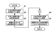
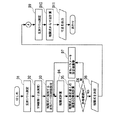
図1は、本発明を実施するための最良の一形態を説明するための図である。図1には、本発明に係る微細構造解析手順の一実施形態が示されている。また、図2は、本発明に係る微細構造体測定方法の一実施形態における、試料測定時の構造体形状と、測定光の反射特性を説明するための断面図である。そして、図3乃至図5は、本発明の一実施の形態に係る微細構造測定方法の原理をさらに詳細に説明するための図である。 FIG. 1 is a diagram for explaining the best mode for carrying out the present invention. FIG. 1 shows an embodiment of a microstructure analysis procedure according to the present invention. Further, FIG. 2 is a cross-sectional view for explaining the structure shape at the time of sample measurement and the reflection characteristic of measurement light in one embodiment of the microstructure measuring method according to the present invention. 3 to 5 are views for explaining the principle of the fine structure measuring method according to the embodiment of the present invention in more detail.
図1を参照して、本発明に係る微細構造解析の一実施の形態の処理手順を説明する。本発明による微細形状の評価手法は、まず、測定する微細形状の寸法が既知である一つ以上の試料表面に測定光を入射し、反射光の反射スペクトルを測定する(ステップA1)。 With reference to FIG. 1, the processing procedure of one embodiment of the fine structure analysis according to the present invention will be described. In the fine shape evaluation method according to the present invention, first, measurement light is incident on one or more sample surfaces whose dimensions of the fine shape to be measured are known, and the reflection spectrum of the reflected light is measured (step A1).
次に、寸法が既知の試料について、測定した微細形状の寸法と、相関関係の強い、反射光スペクトルの特徴(波形パラメータ、例えばピーク強度、波長等)を決定する(ステップA2)。 Next, for a sample with a known dimension, the characteristics of the reflected light spectrum (waveform parameters such as peak intensity, wavelength, etc.) having a strong correlation with the dimension of the measured fine shape are determined (step A2).
さらに、微細形状の寸法と波形パラメータとの関係(相関式あるいは波形解析用のパラメータ)を求める(ステップA3)。 Further, the relationship (correlation equation or waveform analysis parameter) between the dimension of the fine shape and the waveform parameter is obtained (step A3).
次に、寸法が未知な微細構造の表面に測定光入射して、その反射スペクトルを測定する(ステップA4)。 Next, the measurement light is incident on the surface of the fine structure whose dimension is unknown, and the reflection spectrum is measured (step A4).
ステップA3で求めた微細形状の寸法と波形パラメータとの関係(相関式あるいは波形解析用のパラメータ)を用いて、寸法が未知な微細構造の寸法を求める(ステップA5)。 Using the relationship between the dimension of the fine shape obtained in step A3 and the waveform parameter (correlation equation or waveform analysis parameter), the dimension of the microstructure having an unknown dimension is obtained (step A5).
次の試料を測定する場合には、A以下のステップA4、A5を繰り返す。なお、図1に示した処理手順は、測定装置を構成するコンピュータで実行されるプログラムにより実現してもよい。 When measuring the next sample, steps A4 and A5 after A are repeated. Note that the processing procedure shown in FIG. 1 may be realized by a program executed by a computer constituting the measuring apparatus.
本実施の形態が測定の対象としている試料は、半導体基板表面にレジスト等をマスクとして、エッチングにより形成した台形形状を有する回折格子である。図2(a)には、この測定試料1に対して、ハロゲンランプ等の測定光を入射したときに、反射光の様子が示されている。
The sample to be measured in this embodiment is a diffraction grating having a trapezoidal shape formed by etching using a resist or the like as a mask on the surface of a semiconductor substrate. FIG. 2A shows the state of reflected light when measurement light such as a halogen lamp is incident on the
本実施の形態では、測定光を入射したときの反射光として、
・台形形状の山部での反射光11、
・台形形状の谷部での反射光12、
・台形形状の斜面での多重反射光13、および、
・台形形状斜面で反射し、基板内の一部を通過したのち、さらに別の台形形状斜面で反射した多重反射光14、
を考慮し、さらに、
それぞれの反射光の光路長差によって生じる干渉の影響を考慮する。
In the present embodiment, as reflected light when measurement light is incident,
-
-
・ Multiple reflected light 13 on the trapezoidal slope, and
Multiple reflected light 14 that is reflected by a trapezoidal slope, passes through a part of the substrate, and then is reflected by another trapezoidal slope,
In addition,
Consider the influence of interference caused by the optical path length difference of each reflected light.
また、反射光として測定されない散乱光15を考慮する。 Also, consider the scattered light 15 that is not measured as reflected light.
図2(b)に示すような半導体基板等に形成した矩形回折格子構造の反射スペクトルを測定する場合、回折格子の周期dが測定波長に比べて十分小さいときには、回折格子山部での反射光(番号1)と谷部での反射光(番号2)との位相差により反射強度が変化する。すなわち、山部および谷部で反射する光の光路差(2h)によって、両者の位相が同じになる波長では反射率が最大となり、位相が逆になる波長では山谷デューティ比(a:b)に応じて反射率が低減する。 When measuring the reflection spectrum of a rectangular diffraction grating structure formed on a semiconductor substrate or the like as shown in FIG. 2B, the reflected light at the diffraction grating peak is when the period d of the diffraction grating is sufficiently smaller than the measurement wavelength. The reflection intensity varies depending on the phase difference between (No. 1) and the reflected light at the valley (No. 2). That is, due to the optical path difference (2h) of the light reflected at the peaks and troughs, the reflectance becomes maximum at wavelengths where the phases of both are the same, and at the wavelengths where the phases are reversed, the valley duty ratio (a: b) is reached. Accordingly, the reflectance is reduced.
一方、図2(c)に示すような台形形状の回折格子の場合には、図2(a)と同様に、回折格子山部での反射光(番号1)、谷部での反射光(番号2)に加えて、斜面での多重反射光(番号3)の干渉を考慮すれば良い。 On the other hand, in the case of a trapezoidal diffraction grating as shown in FIG. 2 (c), the reflected light at the peak of the diffraction grating (number 1) and the reflected light at the trough (as in FIG. 2A) In addition to the number 2), the interference of the multiple reflected light (number 3) on the slope may be considered.
さらに図2(a)に示した、反射光14および散乱光15の影響を考慮することにより、反射スペクトルが決定されることになる。
Further, the reflection spectrum is determined by considering the influence of the reflected
回折格子による多重反射の影響を評価する方法の一つとして、基板の反射率の波長依存性を利用する方法がある。 One method for evaluating the influence of multiple reflection by a diffraction grating is to use the wavelength dependence of the reflectance of the substrate.
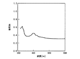
図3は、InP基板についての絶対反射率の波長依存性を示している。250nm付近および400nm付近に極大値を有しており、多重反射成分が大きくなると極大値における反射率が他に比べて大きくなるため、反射スペクトルの極大値から斜面部の割合および角度に依存した多重反射量を測定することが可能となる。 FIG. 3 shows the wavelength dependence of the absolute reflectance for the InP substrate. It has local maximum values in the vicinity of 250 nm and 400 nm, and when the multiple reflection component increases, the reflectance at the local maximum value becomes larger than the others, so that the multiple depending on the ratio and angle of the slope portion from the local maximum value of the reflection spectrum. It is possible to measure the amount of reflection.
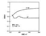
図4は、図2(a)および図2(b)に相当するInP基板に形成した回折格子の反射スペクトルの計算例を示している。図4において、横軸は波長、縦軸はInP基板に対する反射率を示している。回折格子高さは40nm、デューティ比は5:5(1:1)とした。 FIG. 4 shows a calculation example of the reflection spectrum of the diffraction grating formed on the InP substrate corresponding to FIGS. 2 (a) and 2 (b). In FIG. 4, the horizontal axis indicates the wavelength, and the vertical axis indicates the reflectance with respect to the InP substrate. The height of the diffraction grating was 40 nm, and the duty ratio was 5: 5 (1: 1).
斜部の無い矩形回折格子(θ=90°)の場合、山部での反射光と谷部での反射光とが干渉し、測定波長が短くなるほど反射率が低下している。 In the case of a rectangular diffraction grating (θ = 90 °) without an oblique portion, the reflected light at the peak and the reflected light at the valley interfere with each other, and the reflectance decreases as the measurement wavelength becomes shorter.
一方、斜部を有する構造(θ=45°)の場合、多重反射が生じるため約400nm付近に極大値を有する反射スペクトルが得られている。 On the other hand, in the case of a structure having an oblique portion (θ = 45 °), multiple reflection occurs, so that a reflection spectrum having a maximum value in the vicinity of about 400 nm is obtained.
また、回折格子による多重反射の影響を評価する別の方法として、図2(a)に示した反射光14の波長依存性を利用する方法がある。 As another method for evaluating the influence of multiple reflection by the diffraction grating, there is a method using the wavelength dependence of the reflected light 14 shown in FIG.
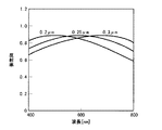
図5は、高さ、山谷デューティ比が同じで、周期のみを0.2μmから0.3μmまで変化させた、InP基板に形成した回折格子の反射スペクトルを示している。多重反射光の光路差による干渉の影響により、周期が長くなるほど極大値が長波長側にシフトした反射スペクトルが得られる。この極大値は山谷デューティ比にも依存し、周期が同じ場合には、屈折率の高い領域の割合が高くなるほど長波長になる。 FIG. 5 shows a reflection spectrum of a diffraction grating formed on an InP substrate with the same height and valley duty ratio and only the period changed from 0.2 μm to 0.3 μm. Due to the influence of interference due to the optical path difference of the multiple reflected light, a reflection spectrum in which the maximum value is shifted to the longer wavelength side as the period becomes longer is obtained. This maximum value also depends on the duty ratio of the valley and valley. When the period is the same, the wavelength becomes longer as the ratio of the region having a higher refractive index becomes higher.
次に、本発明の微細構造測定原理に基づく、測定装置および計算手順の実施例について図面を参照して詳細に説明する。 Next, an embodiment of a measuring apparatus and calculation procedure based on the microstructure measurement principle of the present invention will be described in detail with reference to the drawings.
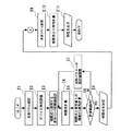
図6は、本発明に係る周期構造測定装置の一実施例の構成を示すブロック図であり、図7は、本発明に係る微細構造測定方法の一実施例の計算手順を説明するためのフローチャートである。 FIG. 6 is a block diagram showing the configuration of an embodiment of the periodic structure measuring apparatus according to the present invention, and FIG. 7 is a flowchart for explaining the calculation procedure of the embodiment of the fine structure measuring method according to the present invention. It is.
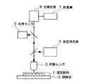
図6を参照すると、本実施例は、測定試料1を設置する試料台2と、測定光を供給するハロゲンランプ等の測定用光源4と、試料に垂直に測定光を入射させ、試料からの反射光を分光して測定する光検出器6、光検出器6で測定されたデータを処理する計算機7とを備えて構成されている。
Referring to FIG. 6, in this embodiment, a sample stage 2 on which a
光検出器6で、試料からの反射光の反射光強度の波長依存性を測定して、計算機7で測定された反射光の反射光強度の波長依存性を解析することで、周期構造を測定する。さらに、測定する領域が狭い場合には、対物レンズ3と、測定領域を観察するための光学モニター5と、を設ける。この構成の場合には、1μm程度の領域の測定が可能となる。
The photodetector 6 measures the wavelength dependence of the reflected light intensity of the reflected light from the sample, and analyzes the wavelength dependence of the reflected light intensity of the reflected light measured by the computer 7 to measure the periodic structure. To do. Furthermore, when the area to be measured is narrow, an
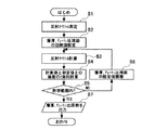
図7に示すフローチャートに従い、本実施例による微細構造の解析手順を説明する。得られた反射光強度の波長依存性を解析する手法としては、まず、微細構造を有する測定試料1を試料台2に設置し、測定用光源4からの測定光を試料に入射し、試料からの反射スペクトルを光検出器6により測定し(ステップB1)、測定した反射スペクトル(測定値)を記憶しておく。
The microstructural analysis procedure according to this embodiment will be described with reference to the flowchart shown in FIG. As a technique for analyzing the wavelength dependence of the obtained reflected light intensity, first, a
次に、計算機7は、測定する周期構造体の高さ、デューティ比、および周期を、任意の値に初期設定し(ステップB2)、初期設定した周期構造体の高さ、デューティ比および周期に基づいて、反射スペクトルを計算する(ステップB3)。周期構造体の高さ、デューティ比、周期から、反射スペクトルを計算により求める。すなわち、微細周期構造を形成した半導体基板に対して、任意の波長の測定光を入射した場合には、回折格子山部での反射光と、谷部での反射光、および、斜面での多重反射光とに光路差に依存した位相差があるため、反射光として観察される光は、それぞれの反射光が干渉したものとなり、半導体および空気層のそれぞれの屈折率に依存する反射と、パタンの形状に依存する散乱光による反射率の低減を考慮した計算により、微細周期構造を形成した半導体基板の反射率を正確に求めることができる。さらに、入射光の波長を変化させた場合について、同様の計算を実施することで、反射スペクトルが計算できる。 Next, the computer 7 initializes the height, duty ratio, and cycle of the periodic structure to be measured to arbitrary values (step B2), and sets the initial height, duty ratio, and cycle of the periodic structure to be measured. Based on this, a reflection spectrum is calculated (step B3). A reflection spectrum is obtained by calculation from the height, duty ratio, and period of the periodic structure. That is, when measurement light of an arbitrary wavelength is incident on a semiconductor substrate having a fine periodic structure, the reflected light at the diffraction grating peak, the reflected light at the valley, and the multiplexing at the inclined surface Since the reflected light has a phase difference depending on the optical path difference, the light observed as the reflected light is the interference of the reflected light, and the reflection depending on the refractive index of the semiconductor and the air layer, and the pattern. The reflectance of the semiconductor substrate on which the fine periodic structure is formed can be accurately obtained by calculation taking into account the reduction of the reflectance due to scattered light depending on the shape of the semiconductor substrate. Further, the reflection spectrum can be calculated by performing the same calculation when the wavelength of the incident light is changed.
次に、計算機7は、ステップB3で計算した反射スペクトルの計算値と、ステップB1で測定した反射スペクトルの測定値とを比較し、反射スペクトルの計算値と測定値との偏差の2乗和を計算する(ステップB4)。 Next, the computer 7 compares the calculated value of the reflection spectrum calculated in step B3 with the measured value of the reflection spectrum measured in step B1, and calculates the sum of squares of the deviation between the calculated value of the reflection spectrum and the measured value. Calculate (step B4).
次に、計算機7は、反射スペクトルの計算値と測定値との偏差の2乗和の値と、反射スペクトルの計算値と測定値との偏差量とが最小値、あるいは予め定められた許容範囲内であるか否かを判断し(ステップB5)、最小値あるいは許容範囲内でない場合には、周期構造体の高さ、デューティ比、および周期の設定値を調整して(ステップB6)、調整した設定値により、ステップB3にて、再度、反射スペクトルを計算する。すなわち、計算機7は、反射スペクトルの計算値と測定値との偏差の2乗和の値が最小になり、かつ反射スペクトルの計算値と測定値との偏差量が十分に小さくなるように周期構造体の高さ、デューティ比、および周期を順次変化させて計算を繰り返す。 Next, the calculator 7 determines that the value of the sum of squares of the deviation between the calculated value and the measured value of the reflection spectrum and the deviation amount between the calculated value and the measured value of the reflected spectrum are the minimum value or a predetermined allowable range. (Step B5), and if not within the minimum value or allowable range, adjust the height, duty ratio, and period set value of the periodic structure (step B6) to adjust Based on the set value, the reflection spectrum is calculated again in step B3. That is, the calculator 7 has a periodic structure so that the sum of squares of the deviation between the calculated value and the measured value of the reflection spectrum is minimized and the deviation amount between the calculated value and the measured value of the reflected spectrum is sufficiently small. The calculation is repeated with the body height, the duty ratio, and the cycle being sequentially changed.
計算機7は、反射スペクトルの計算値と測定値との偏差の2乗和の値と、反射スペクトルの計算値と測定値との偏差量とが予め定められた許容範囲内であると判断した場合には、反射スペクトルの計算値を計算するために設定した周期構造体の高さ、デューティ比および、周期を出力する(ステップB7)。 When the calculator 7 determines that the value of the sum of squares of the deviation between the calculated value and the measured value of the reflection spectrum and the deviation amount between the calculated value and the measured value of the reflected spectrum are within a predetermined allowable range. Output the height, duty ratio, and period of the periodic structure set to calculate the calculated value of the reflection spectrum (step B7).
なお、最初に仮定する、周期構造体の高さ、デューティ比、および周期として、周期構造体の作製時にある程度予想される値、あるいは実測した反射光強度の波長依存性の山谷ピーク位置および強度等から予想される値を用いることで、上記の最小2乗近似は、数秒以下で計算することができる。 Assuming that the height, duty ratio, and period of the periodic structure are initially assumed, values that are expected to some extent when the periodic structure is manufactured, or the peak and valley positions and intensities of the wavelength dependence of the measured reflected light intensity, etc. By using the value expected from the above, the above least square approximation can be calculated in a few seconds or less.
なお、図7に示した処理手順は、計算機7で実行されるプログラムの制御により実現される。 Note that the processing procedure shown in FIG. 7 is realized by control of a program executed by the computer 7.
次に、本発明の実施例として、InP基板上に形成した回折格子パタンの形状を測定する方法について詳細に説明する。 Next, as an embodiment of the present invention, a method for measuring the shape of a diffraction grating pattern formed on an InP substrate will be described in detail.
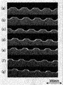
図8は、本発明の実施例で測定した半導体回折格子の断面形状を示す電子顕微鏡写真である。図9は、本発明の実施例で測定した半導体回折格子の反射スペクトルおよびパラメータフィッティング結果(測定値に対する最小2乗近似式)を示す図である。図10(a)は、本発明の実施例で測定した回折格子高さの測定結果を示す図であり、図10(b)は、本発明の実施例で測定した回折格子デューティ比(周期に対する山の割合)の測定結果を示す図である。 FIG. 8 is an electron micrograph showing the cross-sectional shape of the semiconductor diffraction grating measured in the example of the present invention. FIG. 9 is a diagram showing the reflection spectrum of the semiconductor diffraction grating and the parameter fitting result (the least square approximation formula for the measured value) measured in the example of the present invention. FIG. 10A is a diagram showing the measurement result of the diffraction grating height measured in the example of the present invention, and FIG. 10B is a diagram showing the diffraction grating duty ratio (with respect to the period) measured in the example of the present invention. It is a figure which shows the measurement result of the ratio of a mountain.
図8は、本発明の実施例で測定に用いた回折格子の断面SEM写真を示す図であり、電子ビーム(EB)露光により作製した、1.55μm帯DFBレーザの回折格子となる周期が0.240μmのラインアンドスペースパタンである。 FIG. 8 is a diagram showing a cross-sectional SEM photograph of the diffraction grating used in the measurement of the example of the present invention. The period of the diffraction grating of the 1.55 μm band DFB laser produced by electron beam (EB) exposure is 0. 240 μm line and space pattern.
EB露光およびエッチングの条件を変化させることにより、回折格子の高さとデューティ比を意図的に変化させている。 By changing the EB exposure and etching conditions, the height and duty ratio of the diffraction grating are intentionally changed.
図8に示されるように、回折格子を構成する凹凸形状は斜面を有する台形形状となっており、測定光を入射した場合には一部の入射光が多重反射したり、散乱、あるいは回折したりすることが予想される。 As shown in FIG. 8, the concavo-convex shape constituting the diffraction grating is a trapezoidal shape having an inclined surface, and when the measurement light is incident, a part of the incident light is multiple-reflected, scattered or diffracted. Is expected.
図9は、図8に示した高さおよびデューティ比が異なる、複数の回折格子パタンを測定したときの反射光強度の波長依存性を示しており、測定用光源は、無偏光で波長約400nmから800nmのハロゲンランプとし、試料からの反射光を分光することで反射光強度の波長依存性を測定した。また、測定領域は対物レンズを使用して約2μmφとした。また、図9には、回折格子高さ、山谷デューティ比をパラメータとして、測定値に最小2乗フィッティングした曲線を計算結果に合わせて示している。なお、図に示しているフィッティングでは、回折格子の周期が0.24μmと予め判っているために、周期を固定して計算した。 FIG. 9 shows the wavelength dependence of reflected light intensity when measuring a plurality of diffraction grating patterns having different heights and duty ratios shown in FIG. 8, and the measurement light source is non-polarized and has a wavelength of about 400 nm. The wavelength dependence of reflected light intensity was measured by spectroscopically analyzing the reflected light from the sample using a 800 nm halogen lamp. The measurement area was about 2 μmφ using an objective lens. FIG. 9 shows a curve obtained by fitting the measured value to the least square using the height of the diffraction grating and the duty ratio of the valley as parameters. In the fitting shown in the figure, since the period of the diffraction grating was previously known to be 0.24 μm, the calculation was performed with a fixed period.
図9に示されるように、回折格子高さ、および、デューティ比が異なるいずれの形状においても、測定結果のフィッティングが良好に行われている。 As shown in FIG. 9, the fitting of the measurement results is performed well in any shape having a different diffraction grating height and duty ratio.
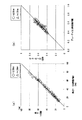
図10(a)および図10(b)には、回折格子の高さおよびデューティ比について、図9に示したフィッティング結果から得られた測定値とSEM観察による実測値との関係を示している。回折格子高さ、デューティ比ともSEM観察値にほぼ一致する値が得られている。 FIG. 10A and FIG. 10B show the relationship between the measured value obtained from the fitting result shown in FIG. 9 and the actually measured value by SEM observation with respect to the height and duty ratio of the diffraction grating. . Both the diffraction grating height and the duty ratio are substantially equal to the SEM observation values.
回折格子高さが30nm以下で測定精度が低下している原因は、反射光による干渉が小さく、スペクトル測定時のノイズ等が影響していることが考えられる。従って、測定回数を増やしノイズの影響を低減すること、あるいはディテクターの感度を向上させることによって測定精度の向上が可能になる。 The reason why the measurement accuracy is lowered when the diffraction grating height is 30 nm or less is considered to be that interference due to reflected light is small and noise or the like at the time of spectrum measurement influences. Therefore, the measurement accuracy can be improved by increasing the number of measurements and reducing the influence of noise, or by improving the sensitivity of the detector.
上述実施例においては、反射光強度を測定している波長を400nmから800nmとしているが、測定波長が短いほど干渉の効果が明瞭に観察されることが多く、測定精度が向上するため、測定波長範囲を広くすることが有効である。測定波長が200nm以下の場合には散乱の影響が大きくなり十分な反射強度が得られないこと、また、波長が800nm以上の場合については、測定精度があまり向上しないことから、実用上は反射光強度測定波長範囲を200nmから800nmとして測定することが有効である。 In the above-described embodiments, the wavelength at which the reflected light intensity is measured is 400 nm to 800 nm. However, the shorter the measurement wavelength, the more clearly the effect of interference is observed, and the measurement accuracy is improved. It is effective to widen the range. When the measurement wavelength is 200 nm or less, the influence of scattering becomes large and sufficient reflection intensity cannot be obtained. When the wavelength is 800 nm or more, the measurement accuracy does not improve so much, so that the reflected light is practically used. It is effective to measure the intensity measurement wavelength range from 200 nm to 800 nm.
また、図6に示した測定計においては、測定試料に対して、測定光を垂直に入射しているが、斜め方向から入射したときの、基板表面での反射光を測定した場合にも同様の解析が可能となる。 In the measuring instrument shown in FIG. 6, the measurement light is perpendicularly incident on the measurement sample. However, the same applies to the case where the reflected light on the substrate surface when incident from an oblique direction is measured. Can be analyzed.
また、上記実施例では、測定光として偏光性の無い光源を使用したが、偏光性のある光源を使用した場合も同様に解析が可能である。 Moreover, in the said Example, although the light source without polarization property was used as measurement light, when a light source with polarization property is used, it can analyze similarly.
次に、本発明の第2の実施例について図面を参照して詳細に説明する。 Next, a second embodiment of the present invention will be described in detail with reference to the drawings.
図11は、本発明に係る微細構造体測定方法における第2の実施例を示す試料測定時の構造体形状と測定光を入射したときの反射特性を示す断面図である。図11に示す構成においては、半導体基板21上に、半導体層A22およびB23を形成した後に、半導体層B23上に微細周期構造を形成している点で、前記第1の実施例と相違している。 FIG. 11 is a cross-sectional view showing the structure shape at the time of sample measurement and the reflection characteristics when measurement light is incident, in the second embodiment of the fine structure measurement method according to the present invention. The configuration shown in FIG. 11 differs from the first embodiment in that a fine periodic structure is formed on the semiconductor layer B23 after the semiconductor layers A22 and B23 are formed on the semiconductor substrate 21. Yes.
本実施例では、測定光を入射したときの反射光として、基板平面部での反射光16に示されるように、
・基板と半導体層Aとの境界での反射、
・半導体層Aと半導体層Bとの境界での反射、
を基板表面での反射と合わせて考慮する必要がある。
In this embodiment, as reflected light when the measurement light is incident, as shown in the reflected light 16 on the substrate plane portion,
-Reflection at the boundary between the substrate and the semiconductor layer A,
Reflection at the boundary between the semiconductor layer A and the semiconductor layer B,
Must be considered together with the reflection on the substrate surface.
回折格子形成領域での反射11〜15についても、図示はしていないが、平面部と同様に、
・基板と半導体層Aとの境界での反射、
・半導体層Aと半導体層Bとの境界での反射、
を考慮することにより、前記第1の実施例と同様に解析することができる。
The
-Reflection at the boundary between the substrate and the semiconductor layer A,
Reflection at the boundary between the semiconductor layer A and the semiconductor layer B,
Can be analyzed in the same manner as in the first embodiment.
まず、平面部での反射スペクトルを測定し、層構造を求め、つぎに、回折格子部の反射スペクトルを測定し、平坦部の測定で得た層構造を考慮することにより微細構造の測定が可能となる。 First, the reflection spectrum at the flat part is measured to obtain the layer structure, then the reflection spectrum at the diffraction grating part is measured, and the fine structure can be measured by considering the layer structure obtained by the measurement of the flat part. It becomes.
本実施例では、台形形状の斜面角度が、前記第1の実施例と相違しており、散乱により測定されない反射光の割合が未知であったため、標準的な形状について、反射スペクトルと断面SEM写真を評価し、散乱光の割合を、まず決定し、散乱光の割合を決定した後に、他の試料の評価を実施した。 In this example, the slope angle of the trapezoidal shape is different from that of the first example, and the ratio of reflected light that is not measured by scattering is unknown. The ratio of scattered light was first determined, and after the ratio of scattered light was determined, the other samples were evaluated.
次に、本発明の微細構造測定原理に基づく計算手順の一実施例を図面に基づいて詳細に説明する。図12は、本発明に係る微細周期構造測定方法における実施例の計算手順を説明するためのフローチャートである。 Next, an embodiment of a calculation procedure based on the microstructure measurement principle of the present invention will be described in detail with reference to the drawings. FIG. 12 is a flowchart for explaining the calculation procedure of the embodiment in the fine periodic structure measuring method according to the present invention.
測定試料の散乱光の割合を求める手法としては、まず、標準的な微細構造を有する測定試料の反射スペクトルを測定する(ステップC1)。 As a method for obtaining the ratio of the scattered light of the measurement sample, first, the reflection spectrum of the measurement sample having a standard fine structure is measured (step C1).
同測定試料の寸法をSEM観察等により測定する(ステップC2)。 The dimension of the measurement sample is measured by SEM observation or the like (step C2).
次に、散乱光の割合を任意の値に初期設定する(ステップC3)。 Next, the ratio of scattered light is initialized to an arbitrary value (step C3).
初期設定した散乱光量、SEM観察により求めた、周期構造体の高さ、デューティ比および周期に基づいて反射スペクトルを計算により求める(ステップC4)。 A reflection spectrum is obtained by calculation based on the initially set amount of scattered light and the height, duty ratio, and period of the periodic structure obtained by SEM observation (step C4).
周期構造体の高さ、デューティ比、周期から反射スペクトルを計算により求める。 A reflection spectrum is obtained by calculation from the height, duty ratio, and period of the periodic structure.
次に、ステップC4で計算した反射スペクトルの計算値と、ステップC1で測定した反射スペクトルの測定値とを比較し、反射スペクトルの計算値と測定値との偏差の2乗和を計算する(ステップC5)。 Next, the calculated value of the reflection spectrum calculated in step C4 is compared with the measured value of the reflection spectrum measured in step C1, and the sum of squares of the deviation between the calculated value of the reflection spectrum and the measured value is calculated (step C5).
反射スペクトルの計算値と測定値との偏差の2乗和の値と、反射スペクトルの計算値と測定値との偏差量とが最小値あるいは予め定められた許容範囲内であるか否かを判断する(ステップC6)。最小値あるいは許容範囲内でない場合には、散乱光の割合を調整して(ステップC7)、調整した設定値によりステップC4で再度反射スペクトルを計算する。 It is determined whether the sum of squares of the deviation between the calculated value of the reflection spectrum and the measured value and the deviation amount between the calculated value of the reflected spectrum and the measured value are within a minimum value or within a predetermined allowable range. (Step C6). If it is not the minimum value or the allowable range, the ratio of scattered light is adjusted (step C7), and the reflection spectrum is calculated again in step C4 with the adjusted set value.
すなわち、反射スペクトルの計算値と測定値との偏差の2乗和の値が最小になり、かつ反射スペクトルの計算値と測定値との偏差量が十分に小さくなるように散乱光の割合を順次変化させて計算を繰り返す。 That is, the ratio of the scattered light is sequentially adjusted so that the sum of squares of the deviation between the calculated value of the reflection spectrum and the measured value is minimized and the deviation amount between the calculated value of the reflected spectrum and the measured value is sufficiently small. Change and repeat the calculation.
反射スペクトルの計算値と測定値との偏差の2乗和の値と、反射スペクトルの計算値と測定値との偏差量とが予め定められた許容範囲内であると判断した場合には、反射スペクトルの計算値を計算するために設定した散乱光の割合を、本実施例で測定する試料についての固定値とする(ステップC8)。 When it is determined that the value of the sum of squares of the deviation between the calculated value of the reflection spectrum and the measured value and the deviation amount between the calculated value of the reflected spectrum and the measured value are within a predetermined allowable range, The ratio of the scattered light set for calculating the calculated value of the spectrum is set as a fixed value for the sample measured in the present example (step C8).
以上の例では、散乱光の割合を決定するための標準サンプルを1試料のみ使用した場合について示しているが、より測定精度を向上させるためには、複数の試料についての反射スペクトルとSEM観察寸法とを使用すれば良い。また、複数の試料について、散乱光の割合を求めた際に、散乱光の割合が他の微細構造の寸法等に依存する場合には、散乱光の割合についての相関式を求めておく。 In the above example, the case where only one standard sample for determining the ratio of scattered light is used is shown. However, in order to improve the measurement accuracy, the reflection spectrum and SEM observation dimensions for a plurality of samples are shown. And can be used. In addition, when the ratio of scattered light is determined for a plurality of samples, if the ratio of scattered light depends on the dimensions of other microstructures, a correlation formula for the ratio of scattered light is determined.
以上の方法で求まった、散乱光量の割合を用いることにより、図12のA以下に示す、図7に示した手順と同じ手順で反射スペクトルから、回折格子の高さ、デューティ比および周期を解析することが可能になる(ステップC9〜C14)。 By using the ratio of the amount of scattered light obtained by the above method, the height, duty ratio and period of the diffraction grating are analyzed from the reflection spectrum in the same procedure as shown in FIG. (Steps C9 to C14).
測定する試料の形状が大きく変わらない場合には、A以下の計算手順を繰り返すことで試料の形状評価が可能となる。 When the shape of the sample to be measured does not change greatly, the shape of the sample can be evaluated by repeating the calculation procedure A and below.
なお、本実施例においては、散乱光の割合が未知である場合について記述しているが、試料の屈折率、あるいは、試料の一部の寸法等が未知である場合についても、同様の方法が適用可能である。 In this embodiment, the case where the ratio of the scattered light is unknown is described. However, the same method can be used when the refractive index of the sample or the size of a part of the sample is unknown. Applicable.
また、散乱光の割合と試料の屈折率等、複数の未知の値がある場合についても同様の方法が適用可能である。その場合、未知の値を求めるための標準サンプル数が多いほど正確な解析が可能となる。 The same method can also be applied when there are a plurality of unknown values such as the ratio of scattered light and the refractive index of the sample. In that case, more accurate analysis becomes possible as the number of standard samples for obtaining an unknown value increases.
なお、図12に示した処理は、測定装置を構成するコンピュータで実行されるプログラムの制御により実現してもよい。 Note that the processing shown in FIG. 12 may be realized by control of a program executed by a computer constituting the measuring apparatus.
また、本実施例においては、図11に示した測定試料についての解析手法を示したが、図2(a)に示した測定試料についても同様に適用可能である。 In the present embodiment, the analysis method for the measurement sample shown in FIG. 11 is shown, but the present invention can be similarly applied to the measurement sample shown in FIG.
次に、本発明の第3の実施例について図面を参照して詳細に説明する。 Next, a third embodiment of the present invention will be described in detail with reference to the drawings.
第1の実施例でも示したように、微細構造体に測定光を入射したときの反射スペクトルは、形状の影響を大きく受け、ピーク波長および強度等に反映される。従って、反射スペクトルの特徴(波形パラメータ)を数式化することにより、制御が必要な寸法をその数式で示すことが可能となる。 As shown in the first embodiment, the reflection spectrum when the measurement light is incident on the fine structure is greatly influenced by the shape, and is reflected in the peak wavelength and the intensity. Therefore, by formulating the characteristic (waveform parameter) of the reflection spectrum, it is possible to indicate the dimension that needs to be controlled by the formula.
図13は、本発明に係る微細構造体測定方法における第3の実施例を示す試料測定時の構造体形状と測定光の反射特性を示す断面図である。図13に示す構成においては、半導体基板21上に、半導体層A22およびB23を形成した後に、半導体層B23上に微細周期構造を形成し、さらに微細構造上に半導体層C24を形成している点で、第2の実施例と異なっている。 FIG. 13 is a cross-sectional view showing the structure shape and the measurement light reflection characteristics during sample measurement in the third embodiment of the fine structure measurement method according to the present invention. In the configuration shown in FIG. 13, after the semiconductor layers A22 and B23 are formed on the semiconductor substrate 21, the fine periodic structure is formed on the semiconductor layer B23, and the semiconductor layer C24 is further formed on the fine structure. This is different from the second embodiment.
本実施例では、試料表面については平坦な形状が得られているが、測定光を入射したときの反射光としては、回折格子形成部での反射、多重反射、および、干渉を考慮し、さらに、図示はしていないが、各層間の境界での多重反射および干渉を考慮することにより、第2の実施例と同様に解析が可能となる。 In this example, a flat shape is obtained on the sample surface, but the reflected light when the measurement light is incident takes into account reflection, multiple reflection, and interference at the diffraction grating forming portion, and further, Although not shown, analysis can be performed in the same manner as in the second embodiment by taking into account multiple reflection and interference at the boundary between layers.
本実施例では、形状が非常に複雑になり、第2の実施例による方法では十分な測定精度が得られなかったため、反射スペクトルと微細構造寸法との相関を求めるために統計的手法を採用した。すなわち、反射スペクトルと微細構造寸法との相関を求めるために、まず、反射スペクトルを測定する可能性のある代表的な形状について、SEM観察等により求めた形状と反射スペクトルを測定し、つぎに反射スペクトルの極値、特性波長での反射強度、特定波長間での強度変化量等を波形パラメータとして相関式を求め、微細構造の寸法測定を実施した。 In this example, the shape is very complicated, and the method according to the second example does not provide sufficient measurement accuracy. Therefore, a statistical method is employed to obtain the correlation between the reflection spectrum and the fine structure size. . That is, in order to obtain the correlation between the reflection spectrum and the fine structure dimension, first, for a representative shape that may be measured for the reflection spectrum, the shape and the reflection spectrum obtained by SEM observation or the like are measured, and then the reflection is measured. Correlation equations were obtained using the waveform extremum, the reflection intensity at the characteristic wavelength, the intensity change between specific wavelengths, etc. as waveform parameters, and the dimensions of the microstructure were measured.
次に、本発明の微細構造測定原理に基づく計算手順を図面に基づいて詳細に説明する。図14は、本発明に係る微細構造測定方法における実施例の計算手順を説明するためのフローチャートである。 Next, a calculation procedure based on the microstructure measurement principle of the present invention will be described in detail with reference to the drawings. FIG. 14 is a flowchart for explaining the calculation procedure of the embodiment in the fine structure measuring method according to the present invention.
まず、複数の測定可能性のある代表的な微細構造を有する測定試料の反射スペクトルを測定する(ステップD1)。次に、ステップD1で反射スペクトルを測定したそれぞれの試料に対応する制御が必要な寸法を、SEM観察等により、測定する(ステップD2)。次に、統計的手法により、相関式に使用する波形パラメータを任意の値に初期設定し(ステップD3)、初期設定した波形パラメータと、ステップD2で測定した、制御が必要な寸法から、相関式を求める(ステップD4)。 First, a reflection spectrum of a measurement sample having a representative fine structure having a plurality of measurement possibilities is measured (step D1). Next, the dimension that requires control corresponding to each sample whose reflection spectrum was measured in step D1 is measured by SEM observation or the like (step D2). Next, the waveform parameter used in the correlation equation is initialized to an arbitrary value by a statistical method (step D3), and the correlation equation is calculated from the initially set waveform parameter and the dimension required for control measured in step D2. Is obtained (step D4).
次に、ステップD4で求めた相関式により得られる寸法と、ステップD2で測定した測定値とを比較し、相関式で得られた寸法と、寸法の測定値との偏差の2乗和を計算する(ステップD5)。相関式により得られる寸法と、測定寸法との偏差の2乗和の値が最小値あるいは予め定められた許容範囲内であるか否かを判断し(ステップD6)、最小値あるいは許容範囲内でない場合には、相関式に使用する波形パラメータを変更して(ステップD7)、ステップD4で再度、相関式を計算する。すなわち、相関式により得られる寸法と測定寸法との偏差の2乗和の値が最小になるように、波形パラメータを順次変化させて、相関式の計算を繰り返す。 Next, the dimension obtained by the correlation equation obtained in step D4 is compared with the measured value measured in step D2, and the sum of squares of the deviation between the dimension obtained by the correlation equation and the measured dimension value is calculated. (Step D5). It is determined whether or not the value of the sum of squares of the deviation between the dimension obtained by the correlation equation and the measured dimension is within the minimum value or a predetermined allowable range (step D6), and is not within the minimum value or the allowable range. In this case, the waveform parameter used for the correlation equation is changed (step D7), and the correlation equation is calculated again in step D4. That is, the calculation of the correlation equation is repeated by sequentially changing the waveform parameters so that the value of the sum of squares of the deviation between the dimension obtained by the correlation equation and the measurement dimension is minimized.
相関式により得られる寸法と測定寸法との偏差の2乗和の値が予め定められた許容範囲内であると判断した場合には、そのときの波形パラメータおよび係数を、反射スペクトルの計算値を計算するために設定した相関式に使用する値として決定する(ステップD8)。 If it is determined that the value of the sum of squares of the deviation between the dimension obtained by the correlation equation and the measured dimension is within a predetermined allowable range, the waveform parameter and coefficient at that time are used as the calculated reflection spectrum. It is determined as a value to be used for the correlation equation set for calculation (step D8).
本実施例では、次のように、相関式の波形パラメータを決定した。 In this example, the waveform parameter of the correlation equation was determined as follows.
波形パラメータとして、ピーク波長(λp)、ピーク強度(Ip)、波長400nmの強度(I1)、波長400nmと450nmの強度の変化量(D1)、波長600nmと650nmの強度の変化量(D2)の5種類の波形パラメータを初期値として用いた。
As waveform parameters, peak wavelength (λ p ), peak intensity (I p ), intensity at
測定が必要な寸法を回折格子の高さである場合、相関式は、a1、a2、a3、a4、a5、を定数として、次のように示される。相関式から求まる回折格子高さをhcとした場合、hcは次式(1)で与えられる。 When the dimension that needs to be measured is the height of the diffraction grating, the correlation equation is expressed as follows, where a 1 , a 2 , a 3 , a 4 , and a 5 are constants. When the height of the diffraction grating obtained from the correlation equation is h c , h c is given by the following equation (1).
hc=a1・λp+a2・Ip+a3・I1+a4・D1+a5・D2 …(1) h c = a 1 · λ p + a 2 · I p + a 3 · I 1 + a 4 · D 1 + a 5 · D 2 (1)
ここで、n個の試料についての反射スペクトル、および、SEM観察した回折格子高さ(hs)がある場合には、下記微分式から、定数a1〜a5を決定することができる。なお、使用する波形パラメータが5種類の場合、nは5以上とする必要があるが、ある程度精度を得るためには、好ましくは、nは20以上とされる。 Here, when there are reflection spectra for n samples and diffraction grating height (h s ) observed by SEM, constants a 1 to a 5 can be determined from the following differential equation. Note that, when five types of waveform parameters are used, n needs to be 5 or more. However, in order to obtain a certain degree of accuracy, n is preferably 20 or more.
Σ(d(hc-hs)2/dλp)=0 …(2) Σ (d (h c -h s ) 2 / dλ p ) = 0 (2)
Σ(d(hc-hs)2/dIp)=0 …(3) Σ (d (h c -h s ) 2 / dI p ) = 0 (3)
Σ(d(hc-hs)2/dI1)=0 …(4) Σ (d (h c -h s ) 2 / dI 1 ) = 0 (4)
Σ(d(hc-hs)2/dD1)=0 …(5) Σ (d (h c -h s ) 2 / dD 1 ) = 0 (5)
Σ(d(hc-hs)2/dD2)=0 …(6) Σ (d (h c -h s ) 2 / dD 2 ) = 0 (6)
ここで、例えば(2)式は、n個の試料についての(hc−hs)2の和をλpで微分した値が0になることを示している。 Here, for example, Expression (2) indicates that the value obtained by differentiating the sum of (h c −h s ) 2 for n samples by λ p is 0.
このように求めた定数を使用して、(1)式から、回折格子高さ(hc)を求めたところ、SEM観察した回折格子高さ(hs)との差が大きく、その差にλpとの相関が見られた。 Using the constants thus determined, the diffraction grating height (h c ) was determined from the equation (1). As a result, the difference from the diffraction grating height (h s ) observed by the SEM was large. the correlation between the λ p was found.
次に、波形パラメータを、ピーク波長(λp)、ピーク波長の2乗(λp 2)、ピーク強度(Ip)、ピーク強度の2乗(Ip 2)、波長400nmの強度(I1)、波長400nmと450nmの強度の変化量(D1)、波長600nmと650nmの強度の変化量(D2)、波長400nmの強度と波長400nmから450nmまでの強度の変化量との積(I1・D1)の積の8種類の値に再設定した。相関式は、上記と同様に、b1からb8を定数として、次のように示される。
Next, the waveform parameters are as follows: peak wavelength (λ p ), peak wavelength square (λ p 2 ), peak intensity (I p ), peak intensity square (I p 2 ), and intensity at
hc=b1・λp+b2・λp 2+b3・Ip+b4・Ip 2+b5・I1+b6・D1+b7・D2+b8・I1・D1 …(7) h c = b 1 • λ p + b 2 • λ p 2 + b 3 • I p + b 4 • I p 2 + b 5 • I 1 + b 6 • D 1 + b 7 • D 2 + b 8 • I 1 • D 1 … ( 7)
ここで、前述の方法と同じ手法で、b1からb8の値を決定することにより、相関式が決定でき、上記(7)式から、回折格子高さを求めたところ、SEM観察した回折格子と良く一致する結果を得た。 Here, the correlation equation can be determined by determining the values of b1 to b8 by the same method as described above, and when the diffraction grating height is obtained from the above equation (7), The results are in good agreement.
以上の方法で求まった、相関式を用いることにより、図14のA以下に示す手順で反射スペクトルから、回折格子の高さを解析することが可能になる(ステップD9〜D11)。測定する試料の形状が大きく変わらない場合には、A以下の計算手順を繰り返すことで試料の形状評価が可能となる。 By using the correlation equation obtained by the above method, the height of the diffraction grating can be analyzed from the reflection spectrum by the procedure shown in FIG. 14A and thereafter (steps D9 to D11). When the shape of the sample to be measured does not change greatly, the shape of the sample can be evaluated by repeating the calculation procedure A and below.
なお、本実施例においては、回折格子高さについて、相関式を求めたが、回折格子デューティ比についても同様の方法で相関式を求めることができる。 In this embodiment, the correlation equation is obtained for the diffraction grating height, but the correlation equation can also be obtained for the diffraction grating duty ratio by the same method.
上記実施例では、回折格子の高さを制御が必要な寸法として取り扱ったが、回折格子高さに相関のあるデバイス特性を制御が必要な値とすることも可能である。 In the above embodiment, the height of the diffraction grating is handled as a dimension that needs to be controlled, but it is also possible to set a device characteristic correlated with the height of the diffraction grating to a value that needs to be controlled.
例えば、半導体レーザでは、図13に示した半導体層の屈折率が同じである場合、回折格子高さはデバイスを評価することにより得られる結合係数と相関があり、発振閾値、スロープ効率とも相関を有している。従って、図15に示すように、SEM観察により寸法を測定する代わりに、デバイス特性を評価する(ステップE2)ことによっても同様に相関式を求めることが可能となる。 For example, in the semiconductor laser, when the refractive index of the semiconductor layer shown in FIG. 13 is the same, the diffraction grating height has a correlation with the coupling coefficient obtained by evaluating the device, and also has a correlation with the oscillation threshold value and the slope efficiency. Have. Therefore, as shown in FIG. 15, instead of measuring the dimensions by SEM observation, it is possible to similarly obtain the correlation equation by evaluating the device characteristics (step E2).
なお、図14、図15に示した処理は、測定装置(解析装置)を構成するコンピュータで実行されるプログラムの制御により実現してもよい。 Note that the processing shown in FIGS. 14 and 15 may be realized by control of a program executed by a computer constituting the measurement apparatus (analysis apparatus).
また、上記実施例では、反射スペクトルのピーク値、特定波長の反射率等を波形パラメータとして取り扱ったが、例えば、得られた反射スペクトルに対して、多項式近似を行い、各項の係数を相関式の波形パラメータとすることも可能である。 In the above embodiment, the peak value of the reflection spectrum, the reflectance at a specific wavelength, and the like are handled as waveform parameters. For example, the obtained reflection spectrum is approximated by a polynomial, and the coefficient of each term is expressed as a correlation equation. It is also possible to use these waveform parameters.
すなわち、得られた反射スペクトルを二次関数で近似したときに、反射強度が、
ax2+bx+c(x:波長、a,b,c:定数)
と示される場合、a,b,cの値を波形パラメータとすることも可能である。
That is, when the obtained reflection spectrum is approximated by a quadratic function, the reflection intensity is
ax 2 + bx + c (x: wavelength, a, b, c: constant)
, The values of a, b, and c can be used as waveform parameters.
また、特定の波長領域での反射スペクトルをそれぞれ多項式で近似することも可能であり、例えば、300nm〜500nmの範囲では、ガウス分布、500から800nmの範囲では、3次多項式で近似し、それぞれの式の係数を波形パラメータとしても良い。 It is also possible to approximate the reflection spectrum in a specific wavelength region by a polynomial, for example, a Gaussian distribution in the range of 300 nm to 500 nm, and a cubic polynomial in the range of 500 to 800 nm. The coefficient of the equation may be used as the waveform parameter.
また、本実施例においては、図13に示した測定試料についての解析手法を示したが、図2(a)に示した測定試料や、図11に示した測定試料についても同様に適用可能である。 In the present embodiment, the analysis method for the measurement sample shown in FIG. 13 is shown. However, the present invention can be similarly applied to the measurement sample shown in FIG. 2A and the measurement sample shown in FIG. is there.
前述した第1から第3の実施例では、光学顕微鏡やレーザ顕微鏡での測定が困難な微細な周期構造パタンの形状を測定することが実現されるが、この方法を用いて周期構造を持たない孤立パタンの寸法を精密に推定することも可能である。すなわち、同じ試料上に同じ手法を用いて孤立パタンと周期構造パタンを同時に作製し、予め両者の相関関係を調べておくことで、周期構造パタンの評価から孤立パタンの形状を測定することができる。 In the first to third embodiments described above, it is possible to measure the shape of a fine periodic structure pattern that is difficult to measure with an optical microscope or a laser microscope, but this method is not used to have a periodic structure. It is also possible to estimate the size of the isolated pattern precisely. That is, it is possible to measure the shape of the isolated pattern from the evaluation of the periodic structure pattern by simultaneously producing the isolated pattern and the periodic structure pattern on the same sample using the same method and examining the correlation between them in advance. .
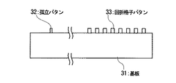
図16は、半導体基板31上に同じ工程により形成した孤立パタン32と回折格子パタン33を示している。EB露光時の近接効果やエッチング時のパタン効果等により孤立パタンと回折格子パタンとで寸法に違いが生じる可能性を考慮して、図17に示すような、予め測定した回折格子パタンと孤立パタンとの関係から、回折格子パタンの形状を本発明により測定することで、孤立パタンの形状を正確に推定することが可能になる。 FIG. 16 shows an isolated pattern 32 and a diffraction grating pattern 33 formed on the semiconductor substrate 31 by the same process. In consideration of the possibility of a difference in size between the isolated pattern and the diffraction grating pattern due to the proximity effect during EB exposure and the pattern effect during etching, etc., the diffraction grating pattern and the isolated pattern measured in advance as shown in FIG. Therefore, by measuring the shape of the diffraction grating pattern according to the present invention, the shape of the isolated pattern can be accurately estimated.
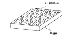
また、上記実施例では、周期構造パタンとして1方向に周期を有する回折格子パタンについて測定したが、2次元の微細構造についても同様に測定可能である。図18は半導体基板上に形成した量子ドットパタンの模式図を示している。GaAs基板上へ10nm前後の横寸法を有するInAs量子ドットを結晶成長時に自己形成したものであるが、量子ドットによる多重反射の影響を反射スペクトルで観察できるため、形状寸法を解析することが可能となる。また、測定する微細構造として周期性が無い場合についても、パタン密度および寸法がある程度そろっていれば解析可能となる。 In the above embodiment, the diffraction grating pattern having a period in one direction is measured as the periodic structure pattern. However, a two-dimensional fine structure can be measured in the same manner. FIG. 18 shows a schematic diagram of a quantum dot pattern formed on a semiconductor substrate. InAs quantum dots having a lateral dimension of about 10 nm on a GaAs substrate are self-formed during crystal growth, but the influence of multiple reflections by the quantum dots can be observed with a reflection spectrum, so that the geometry can be analyzed. Become. In addition, even when there is no periodicity as the microstructure to be measured, it is possible to analyze if the pattern density and dimensions are uniform to some extent.
また、上記実施例では、反射スペクトルについての解析結果を示しているが、透過スペクトルについても同様の解析が適用可能である。 Moreover, although the said Example has shown the analysis result about a reflection spectrum, the same analysis is applicable also about a transmission spectrum.
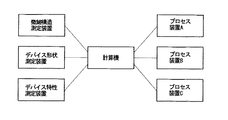
上記実施例では、図6で示したように、試料の反射スペクトルを測定する機能と測定した反射スペクトルを解析する計算機7とが、光学的微細構造測定装置内に近接して設置されている場合を例に説明したが、本発明はかかる構成にのみ限定されるものではない。例えば図19に示すように、微細構造測定装置と計算機とが離れた場所にあり、それらがネットワークにより接続されている場合においても、同様に測定可能である。 In the above embodiment, as shown in FIG. 6, the function for measuring the reflection spectrum of the sample and the computer 7 for analyzing the measured reflection spectrum are installed in the optical fine structure measuring apparatus in the vicinity. However, the present invention is not limited to such a configuration. For example, as shown in FIG. 19, even when the fine structure measuring apparatus and the computer are located at a distance from each other and are connected by a network, the measurement can be performed in the same manner.
この場合、SEM等のデバイス形状測定装置やデバイス特性測定装置についても測定値を計算機にデータ送信できる構造とし、さらに、データ解析した結果を計算機に接続されている他のエッチング装置、露光装置、現像装置などのプロセス装置のプロセス条件へフィードバックすることも実施可能である。また、それぞれの装置がネットワーク接続されておらず、記録メディアを介してデータを受け渡し、離れた場所において測定および解析がそれぞれ実施される場合においても同様に実施可能である。 In this case, the device shape measuring apparatus such as SEM and the device characteristic measuring apparatus are structured so that the measured values can be transmitted to the computer, and the results of the data analysis are further connected to other etching apparatuses, exposure apparatuses, and development devices connected to the computer. It is also possible to feed back to process conditions of process equipment such as equipment. Further, the present invention can be similarly applied when each device is not connected to a network, passes data via a recording medium, and performs measurement and analysis at remote locations.
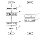
また、測定データの解析のみを実施する、反射スペクトル解析センターを設置し、ネットワーク接続された生産工場との間で、データを送受信するシステムを適用することも可能である。 It is also possible to apply a system that installs a reflection spectrum analysis center that performs only analysis of measurement data and transmits / receives data to / from a network-connected production factory.
図20は、生産工場と反射スペクトル解析センターとのデータ送受信手順を示している。まず、生産工場では、測定する寸法あるいは特性が既知の複数試料の反射波形データを測定する(ステップF1)。 FIG. 20 shows a data transmission / reception procedure between the production factory and the reflection spectrum analysis center. First, the production factory measures the reflected waveform data of a plurality of samples whose dimensions or characteristics to be measured are known (step F1).
該測定データを反射スペクトル解析センターへ送信する(ステップF2)。 The measurement data is transmitted to the reflection spectrum analysis center (step F2).
つぎに、反射スペクトル解析センターに設置されている反射スペクトル解析センター端末でデータ解析を実行する(ステップF3)。 Next, data analysis is performed at the reflection spectrum analysis center terminal installed in the reflection spectrum analysis center (step F3).
解析結果を生産工場へ送信する(ステップF4)。 The analysis result is transmitted to the production factory (step F4).
生産工場では、受け取った解析結果である相関式を微細構造測定装置に解析パラメータとして入力し(ステップF5)、試料の測定を実行する(ステップF6)。 In the production factory, the correlation equation as the received analysis result is input as an analysis parameter to the fine structure measuring apparatus (step F5), and the sample is measured (step F6).
本実施例のシステムは、図14のD3からD8のステップ、あるいは、図15のE3からE8のステップを行うものであり、図14あるいは図15で示したように、いったんパラメータと相関式が決定すれば、A以下のD9からD11のステップ、あるいは、E9からE11のステップを繰り返すことで、工程の寸法管理、あるいはデバイス特性を管理するための寸法管理が実施できるため、解析センターとのデータ送受信を実施するのは、新規試料の測定を実施するときのみである。 The system of this embodiment performs steps D3 to D8 in FIG. 14 or steps E3 to E8 in FIG. 15, and parameters and correlation equations are once determined as shown in FIG. 14 or FIG. By repeating the steps D9 to D11 below A or the steps E9 to E11, process dimension management or dimension management for managing device characteristics can be performed. Is performed only when measuring a new sample.
以上のように、微細構造体の表面に測定光を入射し、反射光強度の波長依存性を、微細構造体の測定表面に平行な面以外での反射および干渉を考慮して解析することにより、微細構造体の形状を非破壊で容易に高精度で測定することが可能になる。 As described above, the measurement light is incident on the surface of the fine structure, and the wavelength dependence of the reflected light intensity is analyzed in consideration of reflection and interference on surfaces other than those parallel to the measurement surface of the fine structure. In addition, the shape of the fine structure can be easily measured with high accuracy in a non-destructive manner.
また、以上のような微細構造解析システムを採用することにより、より高度で正確なデータ処理が可能となり、精密な形状評価が可能となるという効果がある。特に、測定する微細構造の形状が複雑になればなるほど、その効果は顕著である。 Further, by adopting the fine structure analysis system as described above, it is possible to perform higher-level and accurate data processing and to perform accurate shape evaluation. In particular, the effect becomes more remarkable as the shape of the microstructure to be measured becomes more complicated.
本発明は、半導体デバイス製造工程における、リソグラフィ、エッチング、あるいは、結晶成長等により形成する微細構造、すなわち、半導体レーザ等に適用する回折格子構造、量子ドット構造、あるいは、キャパシタ等に適用する凹凸形状を有する粗面の測定に使用される微細構造測定方法およびその方法を用いた微細構造測定装置に適用される。 The present invention provides a fine structure formed by lithography, etching, crystal growth or the like in a semiconductor device manufacturing process, that is, a diffraction grating structure applied to a semiconductor laser, a quantum dot structure, or an uneven shape applied to a capacitor or the like. The present invention is applied to a fine structure measuring method used for measurement of a rough surface having a surface roughness and a fine structure measuring apparatus using the method.
1 測定試料
2 試料台
3 対物レンズ
4 測定用光源
5 光学モニター
6 光検出器
7 計算機
11 台形形状の山部での反射光
12 台形形状の谷部での反射光
13 台形形状の斜面での多重反射光
14 台形形状の斜面での多重反射光
15 散乱光16平面部での多重反射光
21 半導体基板
22 半導体層A
23 半導体層B
24 半導体層C
31 基板
32 孤立パタン
33 回折格子パタン
41 量子ドット
DESCRIPTION OF
23 Semiconductor layer B
24 Semiconductor layer C
31 Substrate 32 Isolated pattern 33 Diffraction grating pattern 41 Quantum dot
Claims (42)
測定する微細形状の寸法が既知である、少なくとも一つの試料に対する反射光強度あるいは透過光強度の波長依存性を測定する工程と、
前記測定する微細形状の寸法と、所定の相関関係を有する、前記反射光強度あるいは透過光強度の波長依存性の特徴(「波形パラメータ」という)を決定する工程と、
前記測定する微細形状の寸法と前記波形パラメータとの関係を求める工程と、
前記測定する微細形状の寸法と前記波形パラメータとの関係を用いて、微細構造の表面に測定光を入射したときの、反射光強度あるいは透過光強度の波長依存性から、前記微細構造の寸法を求める工程と、
を含む、ことを特徴とする微細構造測定方法。 Based on the wavelength dependence of the intensity of reflected light from the microstructure when the measuring light is incident on the surface of the microstructure or the wavelength dependence of the transmitted light intensity that has passed through the microstructure, A microstructure measurement method for measuring,
Measuring the wavelength dependence of reflected light intensity or transmitted light intensity for at least one sample, whose dimensions of the fine shape to be measured are known;
Determining the characteristic of wavelength dependence of the reflected light intensity or transmitted light intensity (referred to as “waveform parameter”) having a predetermined correlation with the dimension of the fine shape to be measured;
Obtaining a relationship between the dimension of the fine shape to be measured and the waveform parameter;
Using the relationship between the dimension of the fine shape to be measured and the waveform parameter, the dimension of the fine structure can be determined from the wavelength dependence of reflected light intensity or transmitted light intensity when measurement light is incident on the surface of the fine structure. The desired process;
A method for measuring a microstructure, comprising:
前記未知の材料物性、あるいは、形状に依存する反射特性を算出する計算工程と、
を含む、ことを特徴とする請求項1乃至3のいずれか一に記載の微細構造測定方法。 Measuring at least one sample of known dimensions to correspond to at least one unknown material property or at least one unknown reflection characteristic depending on shape;
A calculation step of calculating the unknown material properties or reflection characteristics depending on the shape;
The microstructure measurement method according to claim 1, wherein the microstructure measurement method is included.
前記周期構造体の高さ、デューティ比、および、周期を仮定して反射スペクトルの計算値を算出し、前記反射スペクトル測定値と前記反射スペクトル計算値との偏差の2乗和を算出する工程と、
該算出した偏差の2乗和が最小値になるように、前記周期構造体の高さ、デューティ比、および、周期を変化させる工程と、
前記偏差の2乗和が最小値になったときの前記周期構造体の高さ、デューティ比、および、周期を前記周期構造体の形状とする工程と、
を含む、ことを特徴とする微細構造測定方法。 Measuring light incident on the periodic structure, and measuring a reflection spectrum that is wavelength dependence of the intensity of reflected light from the periodic structure; and
Calculating a reflection spectrum calculation value assuming a height, a duty ratio, and a period of the periodic structure, and calculating a sum of squares of a deviation between the reflection spectrum measurement value and the reflection spectrum calculation value; ,
Changing the height, duty ratio, and period of the periodic structure so that the calculated sum of squares of the deviation becomes a minimum value;
The step of setting the height, the duty ratio, and the period of the periodic structure when the sum of squares of the deviation becomes a minimum value to the shape of the periodic structure;
A method for measuring a microstructure, comprising:
前記微細構造体の前記測定を要する箇所の寸法と、少なくとも一つの前記波形パラメータとの相関関係を、所定の統計解析により求める工程と、
を含むことを特徴とする請求項1記載の微細構造測定方法。 A step of measuring the wavelength dependence of the reflected light intensity for a plurality of microstructures whose dimensions need to be measured are known;
Obtaining a correlation between the dimension of the portion requiring the measurement of the microstructure and at least one waveform parameter by a predetermined statistical analysis;
The fine structure measuring method according to claim 1, comprising:
前記微細構造体の前記測定を要する箇所の寸法に依存するデバイスの特性と、前記反射光強度の波長依存性から一意的に決定される、少なくとも一つの前記波形パラメータと、の相関関係を統計解析により求める工程と、
を含む、ことを特徴とする請求項1記載の微細構造測定方法。 Measuring the wavelength dependence of the reflected light intensity for a plurality of microstructures whose physical properties of the device depend on the dimensions of the location requiring measurement; and
Statistical analysis of the correlation between the characteristics of the device depending on the size of the portion requiring measurement of the microstructure and the at least one waveform parameter uniquely determined from the wavelength dependence of the reflected light intensity And the process required by
The fine structure measuring method according to claim 1, comprising:
相関式から求まる、寸法あるいは物理特性と、実測された、寸法あるいは物理特性と、の偏差の2乗和を算出し、該算出した偏差の2乗和が最小値になるように、前記波形パラメータの係数を決定する工程と、
を含む、ことを特徴とする請求項6乃至8のいずれか一に記載の微細構造測定方法。 The size of the part requiring measurement, or the physical property of the device depending on the dimension, and the correlation equation between the waveform parameter and the sum of the waveform parameter multiplied by a coefficient,
The waveform parameter is calculated such that the sum of squares of deviations between the dimensions or physical characteristics obtained from the correlation equation and the actually measured dimensions or physical characteristics is calculated, and the square sum of the calculated deviations becomes a minimum value. Determining a coefficient of
The microstructure measurement method according to claim 6, wherein the microstructure measurement method is included.
前記試料上に前記孤立微細構造と周期構造とを作製する工程と、
前記孤立微細構造と前記周期構造との形状の関係を予め求めておく工程と、
前記周期構造を光学的に測定することにより孤立微細構造の寸法を測定する工程と、
を有する、ことを特徴とする微細構造測定方法。 Measuring structure is incident on the surface of the sample, and based on the reflected light from the sample, the microstructure has a dimension shorter than the wavelength of the measuring light and does not have a periodic structure or a structure conforming to the periodic structure (“isolated microstructure” Is a microstructure measurement method for measuring
Producing the isolated microstructure and the periodic structure on the sample;
Obtaining in advance the relationship between the shape of the isolated fine structure and the periodic structure;
Measuring the dimensions of the isolated microstructure by optically measuring the periodic structure;
A method for measuring a microstructure, characterized by comprising:
測定する微細形状の寸法が既知である、少なくとも一つの試料に対する反射光強度あるいは透過光強度の波長依存性を測定する手段と、
前記測定する微細形状の寸法と所定の相関関係を有する、前記反射光強度あるいは透過光強度の波長依存性の特徴(「波形パラメータ」という)を決定する手段と、
前記測定する微細形状の寸法と前記波形パラメータとの関係を求める手段と、
前記測定する微細形状の寸法と前記波形パラメータとの関係を用いて、微細構造の表面に測定光を入射したときの、反射光強度あるいは透過光強度の波長依存性から、前記微細構造の寸法を求める手段と、
を含む、ことを特徴とする微細構造測定装置。 Based on the wavelength dependence of the intensity of reflected light from the microstructure when the measuring light is incident on the surface of the microstructure or the wavelength dependence of the transmitted light intensity that has passed through the microstructure, A microstructure measuring device for measuring,
Means for measuring the wavelength dependence of reflected light intensity or transmitted light intensity for at least one sample, whose dimensions of the fine shape to be measured are known;
Means for determining a wavelength-dependent characteristic of the reflected light intensity or transmitted light intensity (referred to as “waveform parameter”) having a predetermined correlation with the dimension of the fine shape to be measured;
Means for determining a relationship between the dimension of the fine shape to be measured and the waveform parameter;
Using the relationship between the dimension of the fine shape to be measured and the waveform parameter, the dimension of the fine structure can be determined from the wavelength dependence of reflected light intensity or transmitted light intensity when measurement light is incident on the surface of the fine structure. Means to seek,
A fine structure measuring apparatus comprising:
を含む、ことを特徴とする請求項11記載の微細構造測定装置。 Calculation means for calculating the shape of the fine structure in consideration of reflection other than the plane parallel to the measurement surface of the fine structure, or interference due to the reflection;
The fine structure measuring apparatus according to claim 11, comprising:
前記未知の材料物性、あるいは、形状に依存する反射特性を算出する計算手段と、
を含む、ことを特徴とする請求項11乃至13のいずれか一に記載の微細構造測定装置。 Means for measuring at least one sample of known dimensions to correspond to at least one unknown material property or at least one unknown reflection characteristic depending on the shape;
Calculation means for calculating the unknown material properties or reflection characteristics depending on the shape;
The fine structure measuring apparatus according to claim 11, comprising:
測定光を周期構造体に対して入射し、前記周期構造体からの反射光強度の波長依存性である反射スペクトルを測定する手段と、
前記周期構造体の高さ、デューティ比、および、周期を仮定して反射スペクトルの計算値を算出し、前記反射スペクトル測定値と前記反射スペクトル計算値との偏差の2乗和を算出する手段と、
該算出した偏差の2乗和が最小値になるように、前記周期構造体の高さ、デューティ比、および、周期を変化させる手段と、
前記偏差の2乗和が最小値になったときの前記周期構造体の高さ、デューティ比、および、周期を前記周期構造体の形状とする手段と、
を含む、ことを特徴とする微細構造測定装置。 A fine structure measuring apparatus that enters measurement light on a surface of a fine structure and measures a shape based on reflected light from the fine structure,
Means for making the measurement light incident on the periodic structure and measuring a reflection spectrum which is wavelength dependence of the intensity of reflected light from the periodic structure;
Means for calculating a calculated value of a reflection spectrum assuming a height, a duty ratio, and a period of the periodic structure, and calculating a sum of squares of a deviation between the measured reflection spectrum value and the calculated reflection spectrum value; ,
Means for changing the height, the duty ratio, and the period of the periodic structure so that the sum of squares of the calculated deviation becomes a minimum value;
Means for setting the height of the periodic structure when the sum of squares of the deviation becomes a minimum value, the duty ratio, and the period to the shape of the periodic structure;
A fine structure measuring apparatus comprising:
前記微細構造体の前記測定を要する箇所の寸法と、少なくとも一つの前記波形パラメータとの相関関係を所定の統計解析により求める手段と、
を含むことを特徴とする請求項11記載の微細構造測定装置。 Means for measuring the wavelength dependence of reflected light intensity for a plurality of microstructures whose dimensions need to be measured are known;
Means for obtaining a correlation between a dimension of the portion requiring measurement of the microstructure and at least one waveform parameter by a predetermined statistical analysis;
The fine structure measuring apparatus according to claim 11, comprising:
前記微細構造体の前記測定を要する箇所の寸法に依存するデバイスの特性と、少なくとも一つの前記波形パラメータとの相関関係を統計解析により求める手段と、
を含む、ことを特徴とする請求項11記載の微細構造測定装置。 Means for measuring the wavelength dependence of reflected light intensity for a plurality of microstructures whose physical properties of the device depend on the dimensions of the location requiring measurement,
Means for obtaining, by statistical analysis, a correlation between the characteristics of the device depending on the size of the portion requiring the measurement of the microstructure and at least one waveform parameter;
The fine structure measuring apparatus according to claim 11, comprising:
前記相関式から求まる、寸法あるいは物理特性と、実測された、寸法あるいは物理特性との偏差の2乗和を算出し、該算出した偏差の2乗和が最小値になるように、前記波形パラメータの係数を決定する手段と、
を含む、ことを特徴とする請求項16乃至18のいずれか一に記載の微細構造測定装置。 The size of the part that needs to be measured, or the physical property of the device depending on the dimension, and the correlation equation between the waveform parameter and the means for multiplying each of the waveform parameter by a coefficient,
The waveform parameter is calculated so that the sum of squares of the deviation between the dimension or physical characteristic obtained from the correlation equation and the actually measured dimension or physical characteristic is calculated, and the square sum of the calculated deviation becomes a minimum value. Means for determining a coefficient of
The fine structure measuring apparatus according to claim 16, comprising:
前記試料上に、前記孤立微細構造と周期構造とを作製する手段と、
前記孤立微細構造と前記周期構造との形状の関係を予め求めておく手段と、
前記周期構造を光学的に測定することにより孤立微細構造の寸法を測定する手段と、
を有する、ことを特徴とする微細構造測定装置。 Measuring structure is incident on the surface of the sample, and based on the reflected light from the sample, a fine structure having a dimension shorter than the wavelength of the measuring light or a structure conforming to the periodic structure (“isolated fine structure”) A microstructure measuring device for measuring
Means for producing the isolated microstructure and the periodic structure on the sample;
Means for preliminarily determining the shape relationship between the isolated fine structure and the periodic structure;
Means for measuring the dimensions of the isolated microstructure by optically measuring the periodic structure;
A fine structure measuring apparatus characterized by comprising:
測定する微細形状の寸法が既知である、少なくとも一つの試料に対する反射光強度あるいは透過光強度の波長依存性を測定する処理と、
前記測定する微細形状の寸法と所定の相関関係を有する、前記反射光強度あるいは透過光強度の波長依存性の特徴(「波形パラメータ」という)を決定する処理と、
前記測定する微細形状の寸法と前記波形パラメータとの関係を求める処理と、
前記測定する微細形状の寸法と前記波形パラメータとの関係を用いて、微細構造の表面に測定光を入射したときの、反射光強度あるいは透過光強度の波長依存性から、前記微細構造の寸法を求める処理と、
を実行させるプログラム。 Based on the wavelength dependence of the intensity of reflected light from the microstructure when the measuring light is incident on the surface of the microstructure or the wavelength dependence of the transmitted light intensity that has passed through the microstructure, In the computer that constitutes the microstructure measuring device to measure,
A process for measuring the wavelength dependence of reflected light intensity or transmitted light intensity for at least one sample, whose dimensions of the fine shape to be measured are known;
A process of determining a wavelength-dependent characteristic (referred to as “waveform parameter”) of the reflected light intensity or the transmitted light intensity having a predetermined correlation with the dimension of the fine shape to be measured;
A process for obtaining a relationship between the dimension of the fine shape to be measured and the waveform parameter;
Using the relationship between the dimension of the fine shape to be measured and the waveform parameter, the dimension of the fine structure can be determined from the wavelength dependence of reflected light intensity or transmitted light intensity when measurement light is incident on the surface of the fine structure. The required processing,
A program that executes
前記微細構造体の測定表面に平行な面以外での反射、あるいは、該反射による干渉を考慮して、微細構造体の形状を算出する計算処理を、前記コンピュータに実行させるプログラム。 The program according to claim 21, wherein
A program for causing the computer to execute calculation processing for calculating the shape of a fine structure in consideration of reflection on a surface other than a plane parallel to the measurement surface of the fine structure or interference due to the reflection.
試料表面に対して垂直に測定光を入射したときの、前記測定光に対して垂直な面以外での反射、あるいは、該反射による干渉を考慮して微細構造の形状を算出する計算処理を、前記コンピュータに実行させるプログラム。 The program according to claim 21 or 22,
A calculation process for calculating the shape of the fine structure in consideration of reflection on a surface other than the surface perpendicular to the measurement light when the measurement light is incident on the sample surface or interference due to the reflection, A program to be executed by the computer.
少なくとも一つの未知の材料物性、あるいは、形状に依存する少なくとも一つの未知の反射特性に対応するため、前記寸法が既知の少なくとも一つの試料を測定する処理と、
前記未知の材料物性、あるいは、形状に依存する反射特性を算出する計算処理と、
を前記コンピュータに実行させるプログラム。 The program according to any one of claims 21 to 23,
Processing to measure at least one sample of known dimensions in order to accommodate at least one unknown material property or at least one unknown reflection property depending on the shape;
A calculation process for calculating the unknown material properties or reflection characteristics depending on the shape;
A program for causing the computer to execute.
測定光を周期構造体に対して入射し、前記周期構造体からの反射光強度の波長依存性である反射スペクトルを測定する処理と、
前記周期構造体の高さ、デューティ比、および、周期を仮定して反射スペクトルの計算値を算出し、前記反射スペクトル測定値と前記反射スペクトル計算値との偏差の2乗和を算出する処理と、
該算出した偏差の2乗和が最小値になるように、前記周期構造体の高さ、デューティ比、および、周期を変化させる処理と、
前記偏差の2乗和が最小値になったときの前記周期構造体の高さ、デューティ比、および、周期を前記周期構造体の形状とする処理と、
を実行させるプログラム。 A computer that constitutes a fine structure measuring apparatus that enters measurement light on the surface of the fine structure and measures the shape based on the reflected light from the fine structure,
A process of making the measurement light incident on the periodic structure and measuring a reflection spectrum that is wavelength-dependent of the intensity of reflected light from the periodic structure;
A process of calculating a calculated value of a reflection spectrum assuming a height, a duty ratio, and a period of the periodic structure, and calculating a sum of squares of a deviation between the measured reflection spectrum value and the calculated reflection spectrum value; ,
A process of changing the height, the duty ratio, and the period of the periodic structure so that the calculated sum of squares of the deviation becomes a minimum value;
A process of setting the height, the duty ratio, and the period of the periodic structure when the sum of squares of the deviation becomes a minimum value to the shape of the periodic structure;
A program that executes
測定を要する箇所の寸法が既知である複数の微細構造体について、反射光強度の波長依存性を測定する処理と、
前記微細構造体の前記測定を要する箇所の寸法と、前記反射光強度の波長依存性から一意的に決定される、少なくとも一つの前記波形パラメータとの相関関係を統計解析により求める処理と、
を前記コンピュータに実行させるプログラム。 The program according to claim 21, wherein
A process for measuring the wavelength dependence of the reflected light intensity for a plurality of microstructures whose dimensions need to be measured are known;
Processing for obtaining a correlation between at least one waveform parameter uniquely determined from the wavelength dependence of the reflected light intensity and the size of the portion requiring measurement of the microstructure by statistical analysis;
A program for causing the computer to execute.
測定を要する箇所の寸法に依存するデバイスの物理特性が既知である複数の微細構造体について、反射光強度の波長依存性を測定する処理と、
前記微細構造体の前記測定を要する箇所の寸法に依存するデバイスの特性と、前記反射光強度の波長依存性から一意的に決定される、少なくとも一つの前記波形パラメータとの相関関係を統計解析により求める処理と、
を前記コンピュータに実行させるプログラム。 The program according to claim 21, wherein
A process for measuring the wavelength dependence of reflected light intensity for a plurality of microstructures whose physical characteristics of the device depend on the dimensions of the places requiring measurement,
Statistical analysis of the correlation between at least one waveform parameter uniquely determined from the characteristics of the device depending on the size of the portion requiring measurement of the microstructure and the wavelength dependence of the reflected light intensity The required processing,
A program for causing the computer to execute.
反射光強度の波長依存性から一意的に決定される、少なくとも一つの前記波形パラメータを、前記計算処理により決定する処理を、前記コンピュータに実行させるプログラム。 The program according to any one of claims 22 to 24,
A program that causes the computer to execute a process of determining at least one waveform parameter uniquely determined from the wavelength dependence of reflected light intensity by the calculation process.
測定を要する箇所の寸法、あるいは、寸法に依存するデバイスの物理特性と、前記波形パラメータとの相関式を、波形パラメータのそれぞれに係数をかけ合わせたものの和とする処理と、
前記相関式から求まる、寸法あるいは物理特性と、実測された、寸法あるいは物理特性との偏差の2乗和を算出し、該算出した偏差の2乗和が最小値になるように前記波形パラメータの係数を決定する処理と、
を前記コンピュータに実行させるプログラム。 The program according to any one of claims 26 to 28,
The process of setting the correlation between the physical parameter of the part requiring measurement, or the physical characteristics of the device depending on the dimension, and the waveform parameter, which is obtained by multiplying each of the waveform parameters by a coefficient,
The sum of squares of the deviation between the dimension or physical characteristic obtained from the correlation equation and the actually measured dimension or physical characteristic is calculated, and the waveform parameter is set so that the square sum of the calculated deviation becomes a minimum value. Processing to determine the coefficients;
A program for causing the computer to execute.
前記試料上に作成された前記孤立微細構造と周期構造の形状の関係を予め求めておく処理と、
前記周期構造を光学的に測定することにより前記孤立微細構造の寸法を測定する処理と、
を前記コンピュータに実行させるプログラム。 Measuring structure is incident on the surface of the sample, and based on the reflected light from the sample, the microstructure has a dimension shorter than the wavelength of the measuring light and does not have a periodic structure or a structure conforming to the periodic structure (“isolated microstructure” To the computer that constitutes the fine structure measuring device for measuring
Processing to obtain in advance the relationship between the shape of the isolated microstructure and the periodic structure created on the sample;
Processing to measure the dimensions of the isolated microstructure by optically measuring the periodic structure;
A program for causing the computer to execute.
反射スペクトル測定装置を備えた生産工場に設置される第2の端末と、
を備え、
前記第1、第2の端末が相互に通信接続され、
前記第1の端末は、生産工場から解析を依頼する試料の情報として、複数の試料についての反射スペクトル情報と、前記複数の試料それぞれについての測定を要する箇所の寸法情報と、を含む注文情報を受信して、記憶手段に記憶する手段と、
測定を要する箇所の寸法と、反射スペクトルの波形パラメータと、の相関式を求める解析手段と、
解析結果を前記第2の端末に送信する手段と、
を備えている、ことを特徴とする微細構造解析システム。 A first terminal installed in the reflection spectrum analysis center;
A second terminal installed in a production plant equipped with a reflection spectrum measuring device;
With
The first and second terminals are communicatively connected to each other;
The first terminal includes order information including reflection spectrum information for a plurality of samples and dimensional information of locations where measurement is required for each of the plurality of samples as information on a sample to be analyzed from a production factory. Means for receiving and storing in storage means;
An analysis means for obtaining a correlation formula between the dimension of the portion requiring measurement and the waveform parameter of the reflection spectrum;
Means for transmitting the analysis result to the second terminal;
A fine structure analysis system characterized by comprising:
(A2)前記反射スペクトルから、前記形状の寸法と所定の相関関係を有する前記反射スペクトルの特徴を決定する工程と、
(A3)前記形状の寸法と前記反射スペクトルの特徴との関係を求める工程と、
(A4)形状の寸法が未知な試料に測定光を入射し反射スペクトルを測定する工程と、
(A5)前記(A3)の工程で求めた、前記形状の寸法と前記反射スペクトルの特徴との前記関係を用いて、前記(A4)の工程で測定された前記反射スペクトルから、前記形状の寸法が未知な試料の寸法を求める工程と、
を含む、ことを特徴とする測定方法。 (A1) A step of making a measurement light incident on a sample having a known shape dimension and measuring a reflection spectrum;
(A2) determining a characteristic of the reflection spectrum having a predetermined correlation with the size of the shape from the reflection spectrum;
(A3) obtaining a relationship between the dimension of the shape and the characteristic of the reflection spectrum;
(A4) measuring the reflection spectrum by making the measurement light incident on a sample whose shape dimension is unknown;
(A5) Using the relationship between the dimension of the shape and the characteristic of the reflection spectrum obtained in the process of (A3), the dimension of the shape from the reflection spectrum measured in the process of (A4). A process for determining the dimensions of an unknown sample,
A measuring method characterized by comprising.
(B2)前記試料の形状の寸法パラメータの設定値を初期化する工程と、
(B3)前記設定値に基づき、反射スペクトルを算出する工程と、
(B4)前記(B3)の工程で求められた前記反射スペクトルの計算値と、前記(B1)の工程で測定された前記反射スペクトルの実測値との偏差の2乗和を求める工程と、
(B5)前記偏差の2乗和が所定の許容範囲内であるか否か判定する工程と、
(B6)前記工程(B5)の判定の結果、前記偏差の2乗和が前記所定の許容範囲内にない場合には、前記試料の形状の寸法パラメータの設定値を可変させて、前記(B3)の工程に移行する工程と、
(B7)前記工程(B5)の判定の結果、前記偏差の2乗和が前記所定の許容範囲内の場合には、前記工程(B3)で前記反射スペクトルの算出に用いた前記試料の寸法パラメータを出力する工程と、
を含む、ことを特徴とする測定方法。 (B1) A step of measuring light reflected on the sample and measuring a reflection spectrum;
(B2) initializing a set value of a dimension parameter of the shape of the sample;
(B3) calculating a reflection spectrum based on the set value;
(B4) obtaining a sum of squares of deviations between the calculated value of the reflection spectrum obtained in the step (B3) and the actual measurement value of the reflection spectrum measured in the step (B1);
(B5) determining whether the sum of squares of the deviation is within a predetermined allowable range;
(B6) As a result of the determination in the step (B5), when the sum of squares of the deviation is not within the predetermined allowable range, the set value of the dimension parameter of the shape of the sample is varied, and (B3 ) The process of transitioning to the process of
(B7) As a result of the determination in the step (B5), when the square sum of the deviations is within the predetermined allowable range, the dimension parameter of the sample used in the calculation of the reflection spectrum in the step (B3) A process of outputting
A measuring method characterized by comprising.
(C1)試料に測定光を照射し反射スペクトルを測定する工程と、
(C2)前記試料の寸法を顕微鏡観察で測定する工程と、
(C3)散乱光の割合の設定値を初期化する工程と、
(C4)設定された前記散乱光の割合と、前記顕微鏡観察により求めた試料の寸法とに基づいて、反射スペクトルを算出する工程と、
(C5)前記(C4)の工程で算出された反射スペクトルの計算値と、前記(C1)の工程で測定した反射スペクトルの実測値との偏差の2乗和を計算する工程と、
(C6)前記偏差の2乗和が所定の許容範囲内であるか否か判定する工程と、
(C7)前記工程(C6)の前記判定の結果、前記偏差の2乗和が前記所定の許容範囲内にない場合には、前記散乱光の割合の設定値を可変させて、前記工程(C4)に移行する工程と、
(C8)前記工程(C6)の前記判定の結果、前記偏差の2乗和が前記所定の許容範囲内の場合には、前記工程(C4)で反射スペクトルの計算値を算出するために設定した前記散乱光の割合を、測定する試料についての固定値とする工程と、
を含む、ことを特徴とする測定方法。 In the measurement method of Claim 34, in calculating | requiring the ratio of the scattered light of a measurement sample, before the said process (B1),
(C1) irradiating the sample with measurement light and measuring the reflection spectrum;
(C2) measuring the dimensions of the sample by microscopic observation;
(C3) a step of initializing a set value of the ratio of scattered light;
(C4) calculating a reflection spectrum based on the set ratio of the scattered light and the size of the sample obtained by microscopic observation;
(C5) calculating the sum of squares of the deviation between the calculated value of the reflection spectrum calculated in the step (C4) and the actual value of the reflection spectrum measured in the step (C1);
(C6) determining whether or not the sum of squares of the deviation is within a predetermined allowable range;
(C7) As a result of the determination in the step (C6), when the sum of squares of the deviation is not within the predetermined allowable range, the set value of the ratio of the scattered light is varied, and the step (C4 ) Transition to
(C8) As a result of the determination in the step (C6), when the sum of squares of the deviation is within the predetermined allowable range, it is set in order to calculate the calculated value of the reflection spectrum in the step (C4). A step of setting the ratio of the scattered light to a fixed value for the sample to be measured;
A measuring method characterized by comprising.
(D2)前記試料の寸法を、顕微鏡観察又はデバイス特性評価により取得する工程と、
(D3)相関式に用いられる反射スペクトルの波形パラメータの設定値を初期化する工程と、
(D4)設定された前記波形パラメータと、前記工程(D2)で取得された制御が必要な寸法から相関式を算出する工程と、
(D5)前記(D4)の工程で算出された相関式より得られる寸法と、前記(D2)の工程で得られた測定寸法との偏差の2乗和を計算する工程と、
(D6)前記偏差の2乗和が所定の許容範囲内であるか否か判定する工程と、
(D7)前記工程(D6)の前記判定の結果、前記偏差の2乗和が前記所定の許容範囲内にない場合には、前記相関式に用いる波形パラメータの設定値を可変させて、前記工程(D4)に移行する工程と、
(D8)前記工程(D6)の前記判定の結果、前記偏差の2乗和が前記所定の許容範囲内の場合には、前記工程(D4)で前記相関式の算出に用いた前記波形パラメータを、寸法と波形パラメータの相関式に用いる波形パラメータとして設定する工程と、
(D9)試料に測定光を入射し反射スペクトルを測定する工程と、
(D10)前記(D8)の工程で求めた、前記寸法と波形パラメータの相関式を用いて、前記(D9)の工程で測定された前記反射スペクトルから、前記(D9)の工程で用いた試料の寸法を求める工程と、
を含む、ことを特徴とする測定方法。 (D1) irradiating the sample with measurement light and measuring the reflection spectrum;
(D2) obtaining the dimensions of the sample by microscopic observation or device characteristic evaluation;
(D3) initializing the set values of the waveform parameters of the reflection spectrum used in the correlation equation;
(D4) a step of calculating a correlation equation from the set waveform parameter and the dimension required for control acquired in the step (D2);
(D5) calculating a sum of squares of a deviation between the dimension obtained from the correlation equation calculated in the step (D4) and the measurement dimension obtained in the step (D2);
(D6) determining whether or not the sum of squares of the deviation is within a predetermined allowable range;
(D7) As a result of the determination in the step (D6), when the sum of squares of the deviation is not within the predetermined allowable range, the setting value of the waveform parameter used in the correlation equation is varied, and the step A step of shifting to (D4);
(D8) As a result of the determination in the step (D6), when the sum of squares of the deviation is within the predetermined allowable range, the waveform parameter used in the calculation of the correlation equation in the step (D4) A step of setting as a waveform parameter to be used in a correlation equation between dimensions and waveform parameters;
(D9) a step of measuring light reflected on the sample and measuring a reflection spectrum;
(D10) The sample used in the step (D9) from the reflection spectrum measured in the step (D9) using the correlation equation of the dimensions and waveform parameters obtained in the step (D8). The process of determining the dimensions of
A measuring method characterized by comprising.
前記反射スペクトルから、前記形状の寸法と所定の相関関係を有する前記反射スペクトルの特徴を決定する第2の手段と、
前記形状の寸法と前記反射スペクトルの特徴との関係を求める第3の手段と、
形状の寸法が未知な試料に測定光を入射し反射スペクトルを測定する第4の手段と、
前記第3の手段で求めた、前記形状の寸法と前記反射スペクトルの特徴との前記関係を用いて、前記第4の手段で測定された前記反射スペクトルから、前記形状の寸法が未知な試料の寸法を求める第5の手段と、
を含む、ことを特徴とする測定装置。 A first means for injecting measurement light into a sample having a known shape dimension and measuring a reflection spectrum;
A second means for determining a characteristic of the reflection spectrum having a predetermined correlation with the dimension of the shape from the reflection spectrum;
A third means for determining a relationship between the dimension of the shape and the characteristic of the reflection spectrum;
A fourth means for measuring the reflection spectrum by injecting measurement light into a sample whose shape dimension is unknown;
Using the relationship between the dimension of the shape and the characteristic of the reflection spectrum obtained by the third means, from the reflection spectrum measured by the fourth means, the sample having an unknown shape dimension. A fifth means for determining the dimensions;
A measuring device comprising:
前記試料の形状の寸法パラメータの設定値を初期化する第2の手段と、
前記設定値に基づき、反射スペクトルを算出する第3の手段と、
前記反射スペクトルの計算値と、前記反射スペクトルの実測値との偏差の2乗和を求める第4の手段と、
前記偏差の2乗和が所定の許容範囲内であるか否か判定する第5の手段と、
前記第5の手段による判定の結果、前記偏差の2乗和が前記所定の許容範囲内にない場合には、前記試料の形状の寸法パラメータの設定値を可変させて、前記第3の手段により反射スペクトルを算出し、前記第4の手段、前記第5の手段を実行するように制御する第6の手段と、
前記第5の手段による判定の結果、前記偏差の2乗和が前記所定の許容範囲内の場合には、前記反射スペクトルの算出に用いた前記試料の寸法パラメータを出力する第7手段と、
を含む、ことを特徴とする測定装置。 A first means for entering a measurement light into a sample and measuring a reflection spectrum;
A second means for initializing a set value of a dimensional parameter of the shape of the sample;
A third means for calculating a reflection spectrum based on the set value;
A fourth means for obtaining a sum of squares of deviation between the calculated value of the reflection spectrum and the actually measured value of the reflection spectrum;
Fifth means for determining whether or not the sum of squares of the deviation is within a predetermined allowable range;
As a result of the determination by the fifth means, when the square sum of the deviations is not within the predetermined allowable range, the set value of the dimension parameter of the shape of the sample is varied, and the third means Sixth means for calculating a reflection spectrum and controlling to execute the fourth means and the fifth means;
As a result of the determination by the fifth means, if the sum of squares of the deviation is within the predetermined allowable range, seventh means for outputting the dimension parameter of the sample used for calculating the reflection spectrum;
A measuring device comprising:
試料に測定光を照射し反射スペクトルを測定する手段と、
前記試料の寸法を顕微鏡観察で測定する手段と、
散乱光の割合の設定値を初期化する手段と、
設定された前記散乱光の割合と、前記顕微鏡観察により求めた試料の寸法とに基づいて、反射スペクトルを算出する手段と、
前記反射スペクトルの計算値と、前記反射スペクトルの実測値との偏差の2乗和を計算する計算手段と、
前記偏差の2乗和が所定の許容範囲内であるか否か判定する判定手段と、
前記判定手段による判定の結果、前記偏差の2乗和が前記所定の許容範囲内にない場合には、前記散乱光の割合の設定値を可変させて、前記反射スペクトルを算出する手段で反射スペクトルを算出し、前記計算手段、前記判定手段を実行するように制御する手段と、
前記判定手段による判定の結果、前記偏差の2乗和が前記所定の許容範囲内の場合には、前記反射スペクトルの計算値を算出するために設定した前記散乱光の割合を、測定する試料についての固定値とする手段と、
を含む、ことを特徴とする測定装置。 In the measuring apparatus according to claim 39, as means for obtaining a ratio of scattered light of the measurement sample,
Means for irradiating the sample with measurement light and measuring the reflection spectrum;
Means for measuring the dimensions of the sample by microscopic observation;
Means for initializing the set value of the ratio of scattered light;
Means for calculating a reflection spectrum based on the set ratio of the scattered light and the size of the sample obtained by the microscopic observation;
Calculation means for calculating a sum of squares of deviation between the calculated value of the reflection spectrum and the actually measured value of the reflection spectrum;
Determining means for determining whether or not the sum of squares of the deviation is within a predetermined allowable range;
If the result of determination by the determination means is that the sum of squares of the deviation is not within the predetermined allowable range, the reflection spectrum is calculated by the means for calculating the reflection spectrum by varying the set value of the ratio of the scattered light. And calculating means for controlling to execute the calculating means and the determining means;
As a result of determination by the determination means, when the sum of squares of the deviation is within the predetermined allowable range, the ratio of the scattered light set to calculate the calculated value of the reflection spectrum is measured. Means for a fixed value of
A measuring device comprising:
前記試料の寸法を、顕微鏡観察又はデバイス特性評価により取得する第2の手段と、
相関式に用いられる反射スペクトルの波形パラメータの設定値を初期化する第3の手段と、
設定された前記波形パラメータと、前記顕微鏡観察又はデバイス特性評価により取得された寸法から、相関式を算出する第4の手段と、
前記第4の手段で算出された前記相関式より得られる寸法と、前記第2の手段で取得された寸法との偏差の2乗和を計算する第5の手段と、
前記偏差の2乗和が所定の許容範囲内であるか否か判定する第6の手段と、
前記第6の手段による判定の結果、前記偏差の2乗和が前記所定の許容範囲内にない場合には、前記相関式に用いる波形パラメータの設定値を可変させて、前記第4の手段で相関式を算出し、さらに前記第5、第6の手段を実行するように制御する第7の手段と、
前記第6の手段による前記判定の結果、前記偏差の2乗和が前記所定の許容範囲内の場合には、前記第4の手段で相関式の算出に用いた前記波形パラメータを、寸法と波形パラメータの相関式に用いる波形パラメータとして設定する第8の手段と、
形状の寸法が未知の試料に測定光を入射して反射スペクトルを測定し、前記寸法と波形パラメータの前記相関式を用いて、前記測定された前記反射スペクトルから、形状の寸法が未知の試料の寸法を求める第9の手段と、
を含む、ことを特徴とする測定装置。 A first means for irradiating a sample with measurement light and measuring a reflection spectrum;
A second means for obtaining the dimensions of the sample by microscopic observation or device characteristic evaluation;
A third means for initializing the set values of the waveform parameters of the reflection spectrum used in the correlation equation;
A fourth means for calculating a correlation equation from the set waveform parameter and the dimension acquired by the microscope observation or device characteristic evaluation;
A fifth means for calculating a sum of squares of a deviation between the dimension obtained from the correlation equation calculated by the fourth means and the dimension obtained by the second means;
A sixth means for determining whether or not the sum of squares of the deviation is within a predetermined allowable range;
If the result of determination by the sixth means is that the sum of squares of the deviation is not within the predetermined allowable range, the setting value of the waveform parameter used in the correlation equation is varied, and the fourth means A seventh means for calculating a correlation equation and further controlling the fifth and sixth means;
As a result of the determination by the sixth means, if the square sum of the deviations is within the predetermined allowable range, the waveform parameter used for calculating the correlation equation by the fourth means is the dimension and waveform. An eighth means for setting as a waveform parameter to be used in the parameter correlation equation;
A measurement light is incident on a sample whose shape dimension is unknown, and a reflection spectrum is measured. Using the correlation equation of the dimension and the waveform parameter, the shape of the sample whose shape dimension is unknown is determined from the measured reflection spectrum. A ninth means for determining the dimensions;
A measuring device comprising:
Priority Applications (4)
| Application Number | Priority Date | Filing Date | Title |
|---|---|---|---|
| JP2004105903A JP2005291859A (en) | 2004-03-31 | 2004-03-31 | Fine structure measurement method, fine structure measurement apparatus, and fine structure analysis system |
| US11/087,673 US20050219548A1 (en) | 2004-03-31 | 2005-03-24 | Method of measuring micro-structure, micro-structure measurement apparatus, and micro-structure analytical system |
| EP05007122A EP1591751A3 (en) | 2004-03-31 | 2005-03-31 | Method and apparatus for measuring micro-structure, and micro-structure analytical system |
| US12/230,322 US7580134B2 (en) | 2004-03-31 | 2008-08-27 | Method of measuring micro-structure, micro-structure measurement apparatus, and micro-structure analytical system |
Applications Claiming Priority (1)
| Application Number | Priority Date | Filing Date | Title |
|---|---|---|---|
| JP2004105903A JP2005291859A (en) | 2004-03-31 | 2004-03-31 | Fine structure measurement method, fine structure measurement apparatus, and fine structure analysis system |
Publications (1)
| Publication Number | Publication Date |
|---|---|
| JP2005291859A true JP2005291859A (en) | 2005-10-20 |
Family
ID=34934658
Family Applications (1)
| Application Number | Title | Priority Date | Filing Date |
|---|---|---|---|
| JP2004105903A Pending JP2005291859A (en) | 2004-03-31 | 2004-03-31 | Fine structure measurement method, fine structure measurement apparatus, and fine structure analysis system |
Country Status (3)
| Country | Link |
|---|---|
| US (2) | US20050219548A1 (en) |
| EP (1) | EP1591751A3 (en) |
| JP (1) | JP2005291859A (en) |
Cited By (2)
| Publication number | Priority date | Publication date | Assignee | Title |
|---|---|---|---|---|
| JP2013080831A (en) * | 2011-10-04 | 2013-05-02 | Sumitomo Electric Device Innovations Inc | Semiconductor laser element manufacturing method |
| WO2023127152A1 (en) * | 2021-12-28 | 2023-07-06 | 株式会社ニコン | Optical device and inspection method |
Families Citing this family (11)
| Publication number | Priority date | Publication date | Assignee | Title |
|---|---|---|---|---|
| US8070972B2 (en) * | 2006-03-30 | 2011-12-06 | Tokyo Electron Limited | Etching method and etching apparatus |
| CN102916343B (en) * | 2011-08-05 | 2015-07-15 | 苏州大学 | Production device and production method for quantum dot material |
| JP6602388B6 (en) * | 2015-03-25 | 2020-01-15 | エーエスエムエル ネザーランズ ビー.ブイ. | Metrology method, metrology apparatus, and device manufacturing apparatus |
| JP6871833B2 (en) * | 2017-09-19 | 2021-05-12 | キオクシア株式会社 | Shape measuring device and shape measuring method |
| WO2020042190A1 (en) * | 2018-08-31 | 2020-03-05 | 苏州大学张家港工业技术研究院 | Method and device for measuring microstructure topography based on dispersion spectrum coding |
| CN110514122B (en) * | 2019-09-20 | 2021-04-02 | 成都博奥晶芯生物科技有限公司 | Microarray cover plate two-dimensional detection method and device based on laser displacement sensor |
| CN110514123B (en) * | 2019-09-20 | 2021-04-02 | 成都博奥晶芯生物科技有限公司 | Microstructure two-dimensional detection method and device based on laser displacement sensor |
| CN110926362B (en) * | 2019-11-27 | 2021-07-06 | 中国科学技术大学 | Optical detection method for microstructure with large height-width ratio |
| CN114295908B (en) * | 2021-12-01 | 2023-09-26 | 昆山毅普腾自动化技术有限公司 | Rapid detection method for internal microstructure of nano electronic device based on F-SRU network |
| CN114770224B (en) * | 2022-05-25 | 2024-03-08 | 北京理工大学 | Ultra-precise machining tool mark in-situ detection method |
| CN115876097A (en) * | 2023-03-03 | 2023-03-31 | 广州粤芯半导体技术有限公司 | Method for establishing optical critical dimension database, optical measurement structure and method thereof |
Family Cites Families (9)
| Publication number | Priority date | Publication date | Assignee | Title |
|---|---|---|---|---|
| US4748329A (en) * | 1987-02-17 | 1988-05-31 | Canadian Patents And Development Ltd. | Method for on-line thickness monitoring of a transparent film |
| JPH0224502A (en) * | 1988-07-12 | 1990-01-26 | Dainippon Screen Mfg Co Ltd | Film-thickness measuring method |
| US5607800A (en) * | 1995-02-15 | 1997-03-04 | Lucent Technologies Inc. | Method and arrangement for characterizing micro-size patterns |
| JPH11211421A (en) | 1998-01-27 | 1999-08-06 | Nikon Corp | Device and method for measuring line width |
| US5889592A (en) * | 1998-03-18 | 1999-03-30 | Zawaideh; Emad | Nondestructive optical techniques for simultaneously measuring optical constants and thicknesses of single and multilayer films |
| JP2001217291A (en) | 2000-02-02 | 2001-08-10 | Hitachi Ltd | Method and device for estimating form of rough-face semiconductor thin film and manufacturing method of semiconductor device using them |
| WO2001094881A1 (en) * | 2000-06-02 | 2001-12-13 | Gsi Lumonics Corporation | System of fabricating plane parallel substrates with uniform optical paths |
| GB2385417B (en) * | 2002-03-14 | 2004-01-21 | Taylor Hobson Ltd | Surface profiling apparatus |
| US7019844B2 (en) * | 2002-08-13 | 2006-03-28 | Lam Research Corporation | Method for in-situ monitoring of patterned substrate processing using reflectometry. |
-
2004
- 2004-03-31 JP JP2004105903A patent/JP2005291859A/en active Pending
-
2005
- 2005-03-24 US US11/087,673 patent/US20050219548A1/en not_active Abandoned
- 2005-03-31 EP EP05007122A patent/EP1591751A3/en not_active Withdrawn
-
2008
- 2008-08-27 US US12/230,322 patent/US7580134B2/en active Active
Cited By (2)
| Publication number | Priority date | Publication date | Assignee | Title |
|---|---|---|---|---|
| JP2013080831A (en) * | 2011-10-04 | 2013-05-02 | Sumitomo Electric Device Innovations Inc | Semiconductor laser element manufacturing method |
| WO2023127152A1 (en) * | 2021-12-28 | 2023-07-06 | 株式会社ニコン | Optical device and inspection method |
Also Published As
| Publication number | Publication date |
|---|---|
| US7580134B2 (en) | 2009-08-25 |
| US20090066967A1 (en) | 2009-03-12 |
| US20050219548A1 (en) | 2005-10-06 |
| EP1591751A2 (en) | 2005-11-02 |
| EP1591751A3 (en) | 2008-08-20 |
Similar Documents
| Publication | Publication Date | Title |
|---|---|---|
| US7580134B2 (en) | Method of measuring micro-structure, micro-structure measurement apparatus, and micro-structure analytical system | |
| US7532317B2 (en) | Scatterometry method with characteristic signatures matching | |
| US7394554B2 (en) | Selecting a hypothetical profile to use in optical metrology | |
| US7274472B2 (en) | Resolution enhanced optical metrology | |
| JP5096452B2 (en) | Optimization of diffraction order selection for two-dimensional structures | |
| US6750961B2 (en) | System and method for characterizing macro-grating test patterns in advanced lithography and etch processes | |
| US5867276A (en) | Method for broad wavelength scatterometry | |
| US6928395B2 (en) | Method and system for dynamic learning through a regression-based library generation process | |
| US7046375B2 (en) | Edge roughness measurement in optical metrology | |
| KR101342410B1 (en) | System for measuring a sample with a layer containing a periodic diffracting structure | |
| US20060117293A1 (en) | Method for designing an overlay mark | |
| US20080049214A1 (en) | Measuring Diffractive Structures By Parameterizing Spectral Features | |
| WO2008096364A2 (en) | Method and system for measurng in patterned structures | |
| Germer et al. | Developing an uncertainty analysis for optical scatterometry | |
| US20050275850A1 (en) | Shape roughness measurement in optical metrology | |
| KR20130120470A (en) | Method of determining an asymmetric property of a structure | |
| KR20090023248A (en) | Determining profile parameters of a structure using approximation and fine diffraction models in optical metrology | |
| CN108413883B (en) | System and method for measuring complex structures | |
| TW201921128A (en) | Determining an edge roughness parameter of a periodic structure | |
| US20110114951A1 (en) | Semiconductor device and method for producing the same | |
| TWI777357B (en) | Method and system for ocd metrology, and machine-accessible storage medium | |
| Leach et al. | Advances in calibration methods for micro-and nanoscale surfaces | |
| JP4019714B2 (en) | Periodic structure measuring apparatus and periodic structure measuring method | |
| KR20100000468A (en) | Equipment for manufacturing semiconductor device analyzed layered media dimension and used the same | |
| Zaidi et al. | FTIR based nondestructive method for metrology of depths in poly silicon-filled trenches |
Legal Events
| Date | Code | Title | Description |
|---|---|---|---|
| A711 | Notification of change in applicant |
Free format text: JAPANESE INTERMEDIATE CODE: A712 Effective date: 20060424 |
|
| A621 | Written request for application examination |
Free format text: JAPANESE INTERMEDIATE CODE: A621 Effective date: 20070202 |
|
| A977 | Report on retrieval |
Free format text: JAPANESE INTERMEDIATE CODE: A971007 Effective date: 20090128 |
|
| A131 | Notification of reasons for refusal |
Free format text: JAPANESE INTERMEDIATE CODE: A131 Effective date: 20090714 |
|
| A02 | Decision of refusal |
Free format text: JAPANESE INTERMEDIATE CODE: A02 Effective date: 20091117 |