EP4135036A1 - Halbleiterstruktur und herstellungsverfahren dafür - Google Patents
Halbleiterstruktur und herstellungsverfahren dafür Download PDFInfo
- Publication number
- EP4135036A1 EP4135036A1 EP21870544.0A EP21870544A EP4135036A1 EP 4135036 A1 EP4135036 A1 EP 4135036A1 EP 21870544 A EP21870544 A EP 21870544A EP 4135036 A1 EP4135036 A1 EP 4135036A1
- Authority
- EP
- European Patent Office
- Prior art keywords
- layer
- initial
- dielectric layer
- doped
- sidewalls
- Prior art date
- Legal status (The legal status is an assumption and is not a legal conclusion. Google has not performed a legal analysis and makes no representation as to the accuracy of the status listed.)
- Pending
Links
Images








Classifications
-
- H—ELECTRICITY
- H10—SEMICONDUCTOR DEVICES; ELECTRIC SOLID-STATE DEVICES NOT OTHERWISE PROVIDED FOR
- H10B—ELECTRONIC MEMORY DEVICES
- H10B12/00—Dynamic random access memory [DRAM] devices
- H10B12/30—DRAM devices comprising one-transistor - one-capacitor [1T-1C] memory cells
- H10B12/48—Data lines or contacts therefor
- H10B12/482—Bit lines
-
- H—ELECTRICITY
- H10—SEMICONDUCTOR DEVICES; ELECTRIC SOLID-STATE DEVICES NOT OTHERWISE PROVIDED FOR
- H10B—ELECTRONIC MEMORY DEVICES
- H10B12/00—Dynamic random access memory [DRAM] devices
- H10B12/01—Manufacture or treatment
- H10B12/02—Manufacture or treatment for one transistor one-capacitor [1T-1C] memory cells
- H10B12/03—Making the capacitor or connections thereto
- H10B12/033—Making the capacitor or connections thereto the capacitor extending over the transistor
- H10B12/0335—Making a connection between the transistor and the capacitor, e.g. plug
-
- H—ELECTRICITY
- H10—SEMICONDUCTOR DEVICES; ELECTRIC SOLID-STATE DEVICES NOT OTHERWISE PROVIDED FOR
- H10B—ELECTRONIC MEMORY DEVICES
- H10B12/00—Dynamic random access memory [DRAM] devices
- H10B12/01—Manufacture or treatment
- H10B12/02—Manufacture or treatment for one transistor one-capacitor [1T-1C] memory cells
- H10B12/05—Making the transistor
-
- H—ELECTRICITY
- H10—SEMICONDUCTOR DEVICES; ELECTRIC SOLID-STATE DEVICES NOT OTHERWISE PROVIDED FOR
- H10B—ELECTRONIC MEMORY DEVICES
- H10B12/00—Dynamic random access memory [DRAM] devices
- H10B12/30—DRAM devices comprising one-transistor - one-capacitor [1T-1C] memory cells
- H10B12/31—DRAM devices comprising one-transistor - one-capacitor [1T-1C] memory cells having a storage electrode stacked over the transistor
- H10B12/315—DRAM devices comprising one-transistor - one-capacitor [1T-1C] memory cells having a storage electrode stacked over the transistor with the capacitor higher than a bit line
-
- H—ELECTRICITY
- H10—SEMICONDUCTOR DEVICES; ELECTRIC SOLID-STATE DEVICES NOT OTHERWISE PROVIDED FOR
- H10B—ELECTRONIC MEMORY DEVICES
- H10B12/00—Dynamic random access memory [DRAM] devices
- H10B12/30—DRAM devices comprising one-transistor - one-capacitor [1T-1C] memory cells
- H10B12/48—Data lines or contacts therefor
- H10B12/488—Word lines
-
- H—ELECTRICITY
- H10—SEMICONDUCTOR DEVICES; ELECTRIC SOLID-STATE DEVICES NOT OTHERWISE PROVIDED FOR
- H10D—INORGANIC ELECTRIC SEMICONDUCTOR DEVICES
- H10D30/00—Field-effect transistors [FET]
- H10D30/01—Manufacture or treatment
- H10D30/021—Manufacture or treatment of FETs having insulated gates [IGFET]
- H10D30/025—Manufacture or treatment of FETs having insulated gates [IGFET] of vertical IGFETs
-
- H—ELECTRICITY
- H10—SEMICONDUCTOR DEVICES; ELECTRIC SOLID-STATE DEVICES NOT OTHERWISE PROVIDED FOR
- H10D—INORGANIC ELECTRIC SEMICONDUCTOR DEVICES
- H10D30/00—Field-effect transistors [FET]
- H10D30/60—Insulated-gate field-effect transistors [IGFET]
- H10D30/63—Vertical IGFETs
-
- H—ELECTRICITY
- H10—SEMICONDUCTOR DEVICES; ELECTRIC SOLID-STATE DEVICES NOT OTHERWISE PROVIDED FOR
- H10D—INORGANIC ELECTRIC SEMICONDUCTOR DEVICES
- H10D30/00—Field-effect transistors [FET]
- H10D30/60—Insulated-gate field-effect transistors [IGFET]
- H10D30/67—Thin-film transistors [TFT]
- H10D30/6729—Thin-film transistors [TFT] characterised by the electrodes
- H10D30/673—Thin-film transistors [TFT] characterised by the electrodes characterised by the shapes, relative sizes or dispositions of the gate electrodes
- H10D30/6735—Thin-film transistors [TFT] characterised by the electrodes characterised by the shapes, relative sizes or dispositions of the gate electrodes having gates fully surrounding the channels, e.g. gate-all-around
-
- H—ELECTRICITY
- H10—SEMICONDUCTOR DEVICES; ELECTRIC SOLID-STATE DEVICES NOT OTHERWISE PROVIDED FOR
- H10D—INORGANIC ELECTRIC SEMICONDUCTOR DEVICES
- H10D30/00—Field-effect transistors [FET]
- H10D30/60—Insulated-gate field-effect transistors [IGFET]
- H10D30/67—Thin-film transistors [TFT]
- H10D30/6728—Vertical TFTs
Definitions
- the semiconductor element may include at least one of silicon, carbon, germanium, arsenic, gallium or indium.
- both the bit lines 104 and the semiconductor channels 105 include silicon.
- both the bit lines and the semiconductor channels may include germanium.
- both the bit lines and the semiconductor channels include silicon and germanium.
- both the bit lines and the semiconductor channels include silicon and carbon.
- both the bit lines and the semiconductor channels include arsenic and gallium.
- both the bit lines and the semiconductor channels include gallium and indium.
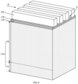
- silicon nitride may be deposited through a chemical vapor deposition process to form the barrier layer 130.
- the silicon nitride film layer is very slow to oxidize, which can protect the substrate 100 located under the silicon nitride film layer and prevent the substrate 100 from being oxidized.
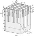
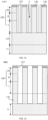
- a fourth dielectric layer 143 is formed in the first trenches a.
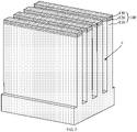
- the fourth dielectric layer 143 is located on sidewalls of the second trenches d (shown in FIG. 9 ), and the fourth dielectric layer 143 is located in the intervals between adjacent semiconductor channels 105.
- the fourth dielectric layer 143 and the fifth dielectric layer 153 form the initial first dielectric layer 113a together, and a fourth interval e is provided between parts of the fifth dielectric layer 153 located on the sidewall of the second trenches d.
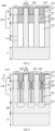
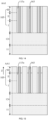
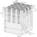
- an orthographic projection of a periphery of the insulating layer 106 on the base 11 is smaller than that of a periphery of the second isolation layer 173 on the base 11. That is, compared to an outer wall of the second isolation layer 173 away from the semiconductor channels 105, an outer wall of the insulating layer 106 away from the semiconductor channels 105 is closer to the semiconductor channels 105. In this way, the fifth intervals i can be formed between the insulating layer 106 and the first isolation layer 163, such that the subsequently formed word lines can surround the part of the insulating layer 106 located on the sidewalls of the channel regions II. In addition, compared to an outer wall of the first dielectric layer 113 (shown in FIG. 20 ) away from the semiconductor channels 105, the outer wall of the insulating layer 106 away from the semiconductor channels 105 may also be closer to the semiconductor channels 105.
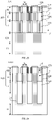
- using the epitaxial growth process is conducive to improving the continuity between the second doped regions III and the initial transition layer 128, reducing contact defects caused by different lattice characteristics or lattice dislocations, reducing contact resistance caused by the contact defects, and improving the transport capacity and moving speed of carriers, thereby improving the conductivity between the second doped regions III and the initial transition layer 128, to reduce the heat generated during the operation of the semiconductor structure;
- using the epitaxial growth process is conducive to increasing the orthographic projection of the initial transition layer 128 on the base 11, making the area of the orthographic projection of a part of the initial transition layer 128 on the base 11 is greater than that of the orthographic projection of the second doped region III on the base 11.
- the remaining part of the first isolation layer 163 is removed to expose the top surfaces of the initial bit lines 124.
Landscapes
- Engineering & Computer Science (AREA)
- Manufacturing & Machinery (AREA)
- Semiconductor Memories (AREA)
- Insulated Gate Type Field-Effect Transistor (AREA)
- Internal Circuitry In Semiconductor Integrated Circuit Devices (AREA)
- Recrystallisation Techniques (AREA)
- Light Receiving Elements (AREA)
- Bipolar Transistors (AREA)
Applications Claiming Priority (2)
| Application Number | Priority Date | Filing Date | Title |
|---|---|---|---|
| CN202110746050.4A CN115568203B (zh) | 2021-07-01 | 2021-07-01 | 半导体结构及其制作方法 |
| PCT/CN2021/121617 WO2023272990A1 (zh) | 2021-07-01 | 2021-09-29 | 半导体结构及其制作方法 |
Publications (2)
| Publication Number | Publication Date |
|---|---|
| EP4135036A1 true EP4135036A1 (de) | 2023-02-15 |
| EP4135036A4 EP4135036A4 (de) | 2023-02-15 |
Family
ID=82115986
Family Applications (1)
| Application Number | Title | Priority Date | Filing Date |
|---|---|---|---|
| EP21870544.0A Pending EP4135036A4 (de) | 2021-07-01 | 2021-09-29 | Halbleiterstruktur und herstellungsverfahren dafür |
Country Status (7)
| Country | Link |
|---|---|
| US (1) | US11600726B2 (de) |
| EP (1) | EP4135036A4 (de) |
| JP (1) | JP7575601B2 (de) |
| KR (1) | KR102768333B1 (de) |
| CN (1) | CN115568203B (de) |
| TW (1) | TWI806672B (de) |
| WO (1) | WO2023272990A1 (de) |
Families Citing this family (6)
| Publication number | Priority date | Publication date | Assignee | Title |
|---|---|---|---|---|
| US20230157003A1 (en) * | 2021-11-12 | 2023-05-18 | Samsung Electronics Co., Ltd. | Semiconductor memory device and method of fabricating the same |
| CN114927477A (zh) * | 2022-05-06 | 2022-08-19 | 长鑫存储技术有限公司 | 一种半导体器件的制备方法、半导体器件及堆叠器件 |
| US12300744B2 (en) * | 2022-06-02 | 2025-05-13 | Changxin Memory Technologies, Inc. | Semiconductor structure and manufacturing method thereof |
| US12464785B2 (en) * | 2022-08-01 | 2025-11-04 | Changxin Memory Technologies, Inc. | Semiconductor structure and method for fabricating same |
| CN116390485B (zh) * | 2023-06-06 | 2023-10-24 | 长鑫存储技术有限公司 | 半导体结构及其制备方法 |
| CN120152273B (zh) * | 2023-12-12 | 2025-12-05 | 长鑫科技集团股份有限公司 | 半导体结构及其制造方法 |
Family Cites Families (43)
| Publication number | Priority date | Publication date | Assignee | Title |
|---|---|---|---|---|
| JP3745392B2 (ja) * | 1994-05-26 | 2006-02-15 | 株式会社ルネサステクノロジ | 半導体装置 |
| US5990509A (en) | 1997-01-22 | 1999-11-23 | International Business Machines Corporation | 2F-square memory cell for gigabit memory applications |
| US7355230B2 (en) | 2004-11-30 | 2008-04-08 | Infineon Technologies Ag | Transistor array for semiconductor memory devices and method for fabricating a vertical channel transistor array |
| KR100673012B1 (ko) | 2005-09-02 | 2007-01-24 | 삼성전자주식회사 | 이중 게이트형 수직 채널 트랜지스터들을 구비하는다이내믹 랜덤 억세스 메모리 장치 및 그 제조 방법 |
| KR20070047572A (ko) * | 2005-11-02 | 2007-05-07 | 삼성전자주식회사 | 반도체 장치 및 그 형성 방법 |
| KR100990549B1 (ko) | 2008-05-02 | 2010-10-29 | 주식회사 하이닉스반도체 | 반도체 소자 및 그 제조 방법 |
| KR100985883B1 (ko) | 2008-06-20 | 2010-10-08 | 주식회사 하이닉스반도체 | 4f2 트랜지스터를 갖는 반도체 소자 및 그 제조방법 |
| KR20100002675A (ko) * | 2008-06-30 | 2010-01-07 | 주식회사 하이닉스반도체 | 반도체 소자의 제조 방법 |
| TWI368315B (en) * | 2008-08-27 | 2012-07-11 | Nanya Technology Corp | Transistor structure, dynamic random access memory containing the transistor structure, and method of making the same |
| US7968876B2 (en) * | 2009-05-22 | 2011-06-28 | Macronix International Co., Ltd. | Phase change memory cell having vertical channel access transistor |
| KR101149043B1 (ko) * | 2009-10-30 | 2012-05-24 | 에스케이하이닉스 주식회사 | 매립형 비트라인을 구비하는 반도체 장치 및 그 제조방법 |
| KR101778287B1 (ko) * | 2010-08-30 | 2017-09-14 | 삼성전자주식회사 | 반도체 메모리 소자 및 그 제조방법 |
| KR101133701B1 (ko) | 2010-09-10 | 2012-04-06 | 주식회사 하이닉스반도체 | 매립비트라인을 구비한 반도체장치 제조 방법 |
| US20120080725A1 (en) | 2010-09-30 | 2012-04-05 | Seagate Technology Llc | Vertical transistor memory array |
| KR101820022B1 (ko) | 2010-11-11 | 2018-01-19 | 삼성전자주식회사 | 수직 채널 트랜지스터를 갖는 반도체 소자 및 그 제조방법 |
| KR101802220B1 (ko) | 2010-12-20 | 2017-11-29 | 삼성전자주식회사 | 수직형 채널 트랜지스터를 포함하는 반도체 소자 및 그 제조 방법 |
| KR101172272B1 (ko) * | 2010-12-30 | 2012-08-09 | 에스케이하이닉스 주식회사 | 매립비트라인을 구비한 반도체장치 제조 방법 |
| US8530312B2 (en) * | 2011-08-08 | 2013-09-10 | Micron Technology, Inc. | Vertical devices and methods of forming |
| TW201322255A (zh) * | 2011-11-21 | 2013-06-01 | Inotera Memories Inc | 動態隨機存取記憶體結構及其製作方法 |
| KR20130075348A (ko) | 2011-12-27 | 2013-07-05 | 에스케이하이닉스 주식회사 | 매립비트라인을 구비한 반도체장치 및 그 제조 방법 |
| KR20130103942A (ko) * | 2012-03-12 | 2013-09-25 | 에스케이하이닉스 주식회사 | 무접합 수직 게이트 트랜지스터를 갖는 반도체 소자 및 그 제조 방법 |
| US9023723B2 (en) * | 2012-05-31 | 2015-05-05 | Applied Materials, Inc. | Method of fabricating a gate-all-around word line for a vertical channel DRAM |
| KR101925012B1 (ko) * | 2012-07-17 | 2018-12-05 | 에스케이하이닉스 주식회사 | 반도체 장치 및 그의 제조 방법 |
| KR20160006466A (ko) * | 2014-07-09 | 2016-01-19 | 에스케이하이닉스 주식회사 | 수직 채널을 갖는 반도체 집적 회로 장치 및 그 제조방법 |
| US9646973B2 (en) * | 2015-03-27 | 2017-05-09 | Taiwan Semiconductor Manufacturing Company, Ltd. | Dual-port SRAM cell structure with vertical devices |
| KR101750093B1 (ko) * | 2016-11-30 | 2017-07-04 | 삼성전자주식회사 | 수직 채널 트랜지스터의 제조방법 |
| EP3435413A1 (de) * | 2017-07-28 | 2019-01-30 | IMEC vzw | Halbleiterbauelement und verfahren zur herstellung des halbleiterbauelements |
| CN109461756B (zh) * | 2017-09-06 | 2021-05-14 | 中国科学院微电子研究所 | Mram及其制造方法及包括mram的电子设备 |
| CN109461738B (zh) | 2017-09-06 | 2021-03-26 | 中国科学院微电子研究所 | 半导体存储设备及其制造方法及包括存储设备的电子设备 |
| TWI653712B (zh) | 2017-11-07 | 2019-03-11 | 華邦電子股份有限公司 | 半導體結構及其製造方法 |
| CN108461496B (zh) * | 2018-05-09 | 2023-09-29 | 长鑫存储技术有限公司 | 集成电路存储器及其形成方法、半导体集成电路器件 |
| CN108493188B (zh) | 2018-05-09 | 2023-10-13 | 长鑫存储技术有限公司 | 集成电路存储器及其形成方法、半导体集成电路器件 |
| CN208127209U (zh) * | 2018-05-09 | 2018-11-20 | 长鑫存储技术有限公司 | 集成电路存储器及半导体集成电路器件 |
| CN109285836B (zh) * | 2018-08-28 | 2023-10-10 | 中国科学院微电子研究所 | 半导体存储设备及其制造方法及包括存储设备的电子设备 |
| CN208655642U (zh) * | 2018-09-05 | 2019-03-26 | 长鑫存储技术有限公司 | 半导体存储器 |
| CN110957319A (zh) | 2018-09-27 | 2020-04-03 | 长鑫存储技术有限公司 | 集成电路存储器及其形成方法、半导体集成电路器件 |
| CN111354738A (zh) | 2018-12-21 | 2020-06-30 | 芯恩(青岛)集成电路有限公司 | 一种三维有结半导体存储器件及其制造方法 |
| US10629615B1 (en) | 2019-01-04 | 2020-04-21 | Macronix International Co., Ltd. | Semiconductor structure having doped active pillars in trenches |
| CN111834338B (zh) * | 2019-04-22 | 2025-01-10 | 长鑫存储技术有限公司 | 电容器及其形成方法、dram单元和存储器 |
| KR102713747B1 (ko) | 2019-07-26 | 2024-10-08 | 에스케이하이닉스 주식회사 | 수직형 메모리 장치 및 수직형 메모리 장치 제조 방법 |
| US11315936B2 (en) | 2019-08-29 | 2022-04-26 | Taiwan Semiconductor Manufacturing Company, Ltd. | Memory device and manufacturing method thereof |
| US11049862B2 (en) * | 2019-10-20 | 2021-06-29 | HeFeChip Corporation Limited | Semiconductor device and fabrication method thereof |
| CN211719592U (zh) | 2020-04-27 | 2020-10-20 | 长鑫存储技术有限公司 | 半导体结构和存储器 |
-
2021
- 2021-07-01 CN CN202110746050.4A patent/CN115568203B/zh active Active
- 2021-09-29 KR KR1020237018424A patent/KR102768333B1/ko active Active
- 2021-09-29 JP JP2023532840A patent/JP7575601B2/ja active Active
- 2021-09-29 WO PCT/CN2021/121617 patent/WO2023272990A1/zh not_active Ceased
- 2021-09-29 EP EP21870544.0A patent/EP4135036A4/de active Pending
-
2022
- 2022-01-24 US US17/648,732 patent/US11600726B2/en active Active
- 2022-06-22 TW TW111123244A patent/TWI806672B/zh active
Also Published As
| Publication number | Publication date |
|---|---|
| KR102768333B1 (ko) | 2025-02-18 |
| JP2023551332A (ja) | 2023-12-07 |
| WO2023272990A1 (zh) | 2023-01-05 |
| JP7575601B2 (ja) | 2024-10-29 |
| EP4135036A4 (de) | 2023-02-15 |
| TWI806672B (zh) | 2023-06-21 |
| CN115568203B (zh) | 2025-08-15 |
| CN115568203A (zh) | 2023-01-03 |
| KR20230093335A (ko) | 2023-06-27 |
| US11600726B2 (en) | 2023-03-07 |
| TW202303933A (zh) | 2023-01-16 |
| US20230006061A1 (en) | 2023-01-05 |
Similar Documents
| Publication | Publication Date | Title |
|---|---|---|
| US11600726B2 (en) | Semiconductor structure | |
| EP4231342B1 (de) | Halbleiterstruktur und herstellungsverfahren dafür | |
| US11569240B2 (en) | Semiconductor structure and manufacturing method thereof | |
| CN115701211B (zh) | 半导体结构及其制作方法 | |
| CN115939043B (zh) | 半导体结构及其制作方法 | |
| US12114485B2 (en) | Semiconductor structure and method for manufacturing same | |
| TWI802451B (zh) | 半導體結構及其製造方法 | |
| CN111916399B (zh) | 一种半导体器件的制备方法以及半导体器件 | |
| WO2023133993A1 (zh) | 半导体结构及半导体结构的制备方法 | |
| RU2807501C1 (ru) | Полупроводниковая структура и способ ее изготовления | |
| US12414285B2 (en) | Semiconductor structure and manufacturing method thereof |
Legal Events
| Date | Code | Title | Description |
|---|---|---|---|
| STAA | Information on the status of an ep patent application or granted ep patent |
Free format text: STATUS: UNKNOWN |
|
| STAA | Information on the status of an ep patent application or granted ep patent |
Free format text: STATUS: THE INTERNATIONAL PUBLICATION HAS BEEN MADE |
|
| PUAI | Public reference made under article 153(3) epc to a published international application that has entered the european phase |
Free format text: ORIGINAL CODE: 0009012 |
|
| STAA | Information on the status of an ep patent application or granted ep patent |
Free format text: STATUS: REQUEST FOR EXAMINATION WAS MADE |
|
| 17P | Request for examination filed |
Effective date: 20220331 |
|
| A4 | Supplementary search report drawn up and despatched |
Effective date: 20221213 |
|
| AK | Designated contracting states |
Kind code of ref document: A1 Designated state(s): AL AT BE BG CH CY CZ DE DK EE ES FI FR GB GR HR HU IE IS IT LI LT LU LV MC MK MT NL NO PL PT RO RS SE SI SK SM TR |
|
| DAV | Request for validation of the european patent (deleted) | ||
| DAX | Request for extension of the european patent (deleted) |