EP4024892B1 - Signalverarbeitungsvorrichtung und einstellverfahren - Google Patents
Signalverarbeitungsvorrichtung und einstellverfahren Download PDFInfo
- Publication number
- EP4024892B1 EP4024892B1 EP20857297.4A EP20857297A EP4024892B1 EP 4024892 B1 EP4024892 B1 EP 4024892B1 EP 20857297 A EP20857297 A EP 20857297A EP 4024892 B1 EP4024892 B1 EP 4024892B1
- Authority
- EP
- European Patent Office
- Prior art keywords
- signal
- adjuster
- input
- output
- offset
- Prior art date
- Legal status (The legal status is an assumption and is not a legal conclusion. Google has not performed a legal analysis and makes no representation as to the accuracy of the status listed.)
- Active
Links
Images


Classifications
-
- H—ELECTRICITY
- H03—ELECTRONIC CIRCUITRY
- H03F—AMPLIFIERS
- H03F3/00—Amplifiers with only discharge tubes or only semiconductor devices as amplifying elements
- H03F3/20—Power amplifiers, e.g. Class B amplifiers, Class C amplifiers
- H03F3/21—Power amplifiers, e.g. Class B amplifiers, Class C amplifiers with semiconductor devices only
- H03F3/217—Class D power amplifiers; Switching amplifiers
-
- H—ELECTRICITY
- H03—ELECTRONIC CIRCUITRY
- H03F—AMPLIFIERS
- H03F1/00—Details of amplifiers with only discharge tubes, only semiconductor devices or only unspecified devices as amplifying elements
- H03F1/32—Modifications of amplifiers to reduce non-linear distortion
- H03F1/3241—Modifications of amplifiers to reduce non-linear distortion using predistortion circuits
- H03F1/3247—Modifications of amplifiers to reduce non-linear distortion using predistortion circuits using feedback acting on predistortion circuits
-
- H—ELECTRICITY
- H03—ELECTRONIC CIRCUITRY
- H03F—AMPLIFIERS
- H03F1/00—Details of amplifiers with only discharge tubes, only semiconductor devices or only unspecified devices as amplifying elements
- H03F1/30—Modifications of amplifiers to reduce influence of variations of temperature or supply voltage or other physical parameters
- H03F1/301—Modifications of amplifiers to reduce influence of variations of temperature or supply voltage or other physical parameters in MOSFET amplifiers
-
- H—ELECTRICITY
- H03—ELECTRONIC CIRCUITRY
- H03F—AMPLIFIERS
- H03F1/00—Details of amplifiers with only discharge tubes, only semiconductor devices or only unspecified devices as amplifying elements
- H03F1/32—Modifications of amplifiers to reduce non-linear distortion
- H03F1/3241—Modifications of amplifiers to reduce non-linear distortion using predistortion circuits
- H03F1/3264—Modifications of amplifiers to reduce non-linear distortion using predistortion circuits in audio amplifiers
-
- H—ELECTRICITY
- H03—ELECTRONIC CIRCUITRY
- H03F—AMPLIFIERS
- H03F3/00—Amplifiers with only discharge tubes or only semiconductor devices as amplifying elements
- H03F3/181—Low-frequency amplifiers, e.g. audio preamplifiers
- H03F3/183—Low-frequency amplifiers, e.g. audio preamplifiers with semiconductor devices only
- H03F3/187—Low-frequency amplifiers, e.g. audio preamplifiers with semiconductor devices only in integrated circuits
-
- H—ELECTRICITY
- H03—ELECTRONIC CIRCUITRY
- H03F—AMPLIFIERS
- H03F3/00—Amplifiers with only discharge tubes or only semiconductor devices as amplifying elements
- H03F3/20—Power amplifiers, e.g. Class B amplifiers, Class C amplifiers
- H03F3/21—Power amplifiers, e.g. Class B amplifiers, Class C amplifiers with semiconductor devices only
- H03F3/217—Class D power amplifiers; Switching amplifiers
- H03F3/2175—Class D power amplifiers; Switching amplifiers using analogue-digital or digital-analogue conversion
-
- H—ELECTRICITY
- H04—ELECTRIC COMMUNICATION TECHNIQUE
- H04R—LOUDSPEAKERS, MICROPHONES, GRAMOPHONE PICK-UPS OR LIKE ACOUSTIC ELECTROMECHANICAL TRANSDUCERS; DEAF-AID SETS; PUBLIC ADDRESS SYSTEMS
- H04R3/00—Circuits for transducers, loudspeakers or microphones
- H04R3/04—Circuits for transducers, loudspeakers or microphones for correcting frequency response
-
- H—ELECTRICITY
- H03—ELECTRONIC CIRCUITRY
- H03F—AMPLIFIERS
- H03F2200/00—Indexing scheme relating to amplifiers
- H03F2200/03—Indexing scheme relating to amplifiers the amplifier being designed for audio applications
-
- H—ELECTRICITY
- H03—ELECTRONIC CIRCUITRY
- H03F—AMPLIFIERS
- H03F2200/00—Indexing scheme relating to amplifiers
- H03F2200/331—Sigma delta modulation being used in an amplifying circuit
-
- H—ELECTRICITY
- H03—ELECTRONIC CIRCUITRY
- H03F—AMPLIFIERS
- H03F2200/00—Indexing scheme relating to amplifiers
- H03F2200/351—Pulse width modulation being used in an amplifying circuit
-
- H—ELECTRICITY
- H03—ELECTRONIC CIRCUITRY
- H03F—AMPLIFIERS
- H03F2200/00—Indexing scheme relating to amplifiers
- H03F2200/391—Indexing scheme relating to amplifiers the output circuit of an amplifying stage comprising an LC-network
-
- H—ELECTRICITY
- H04—ELECTRIC COMMUNICATION TECHNIQUE
- H04R—LOUDSPEAKERS, MICROPHONES, GRAMOPHONE PICK-UPS OR LIKE ACOUSTIC ELECTROMECHANICAL TRANSDUCERS; DEAF-AID SETS; PUBLIC ADDRESS SYSTEMS
- H04R3/00—Circuits for transducers, loudspeakers or microphones
- H04R3/007—Protection circuits for transducers
Definitions
- the present disclosure relates to a signal processing device that amplifies a digital audio signal and a method for adjusting parameters of the signal processing device.
- an amplifier also referred to as a full digital amplifier
- a full digital amplifier which does not convert a digital audio signal into an analog signal, but directly generates a switching signal by digital modulation and amplifies the digital signal as is, has been developed.
- the driver circuit switches directly to the power supply circuit, the waveform of the power supply noise appears at the amplifier output due to the mixing of the power supply noise.
- the switching transistor a metal oxide semiconductor field effect transistor (MOSFET) or the like capable of high-speed response is used.
- MOSFET metal oxide semiconductor field effect transistor
- PTL 3 discloses a signal processing device in which distortion and noise in high power digital PWM amplifiers is reduced by measuring the difference between the desired output signal and the actual output signal on a pulse by pulse basis. This analog error is converted into a digital signal with an analog to digital converter (ADC). The digital error signal is then used to correct the feedback of the delta sigma modulator in real time.
- ADC analog to digital converter
- the amplitude, DC offset and the like of the signal that is to be fed back need to be adjusted.
- a method of making the adjustment a method of using a variable resistor can be considered.
- the resistance value shifts due to aged deterioration of the variable resistor, and the resistance value also shifts due to an impact such as vibration.
- the adjustment varies depending on the person making the adjustment. In this way, in the method using a variable resistor, it is difficult to accurately adjust the amplitude and DC offset of the signal that is to be fed back, that is, it is difficult to accurately extract the distortion component.
- the present disclosure provides a signal processing device or the like capable of more accurately extracting distortion components using feedback technology.
- the signal processing device in the present disclosure is defined by the independent claim 1.
- a corresponding method for adjusting parameters for the signal processing device is defined by the independent claim 6.
- Further embodiments are defined by the appended dependent claims.
- the distortion component can be extracted more accurately by using the feedback technology.
- FIG. 1 is a configuration diagram showing an example of signal processing device 1 according to the embodiment.
- FIG. 1 shows no-signal generator 110, test signal generator 120, and speaker 130. No-signal generator 110, test signal generator 120, and speaker 130 may be provided in signal processing device 1.
- Signal processing device 1 is a device that inputs a digital audio signal obtained from a music source, processes the digital audio signal, and outputs an analog signal to speaker 130 in order to reproduce the music source stored in a storage medium such as a compact disc (CD), a digital versatile disc (DVD), a Blu-ray (registered trademark) disc (BD), a hard disc drive (HDD) or the like.
- a storage medium such as a compact disc (CD), a digital versatile disc (DVD), a Blu-ray (registered trademark) disc (BD), a hard disc drive (HDD) or the like.
- Subtractor 10 is a circuit that subtracts a feedback signal from an input signal that is a digital audio signal and outputs a first digital signal.
- the feedback signal is a signal generated by feeding back an analog signal output from power amplifier circuit 30 and performing various signal processing.
- the feedback signal is a signal that is obtained by processing an analog signal by analog LPF 41, A/D converter 40, offset adjuster 51, amplitude adjuster 52, subtractor 71, compensation filter 72 and decimation filter 73, and is output from decimation filter 73.
- the feedback signal includes a distortion component generated by power amplifier circuit 30 or the like, and the distortion component generated by power amplifier circuit 30 or the like can be canceled by subtracting the distortion component in advance in subtractor 10.
- Signal processing circuit 20 is a circuit that performs signal processing on the first digital signal and outputs the second digital signal.
- Signal processing circuit 20 includes ⁇ modulator 21 and pulse width modulation (PWM) modulator 22.
- ⁇ modulator 21 requantizes the number of gradations of the pulse width of PWM modulator 22 which is smaller than the input audio signal. Due to the feature of the noise shaping of the ⁇ -modulation that pushes the re-quantization noise out of the audible band of, for example, 20 kHz or more, the re-quantization noise generated at the time of re-quantization is reduced in the audible band.
- PWM modulator 22 converts a signal output by ⁇ modulator 21 to a second digital signal (pulse width modulated signal) having the gradation of the pulse width represented by two values of 1 and 0 or 1 and -1 for the gradation of the amplitude level of the signal.
- the second digital signal contains a distortion component when it is amplified by power amplifier circuit 30 and converted into an analog signal.
- the difference between the signals before and after the distortion component is superimposed is extracted.
- the second digital signal before the distortion component is superimposed is input to subtractor 71.
- Power amplifier circuit 30 is a circuit that amplifies the signal amplitude of the second digital signal, converts the amplified second digital signal into an analog signal, and outputs the analog signal.
- Power amplifier circuit 30 includes driver circuit 31, switching transistors 32 and 33, and low pass filter (LPF) 34. It should be noted that power amplifier circuit 30 is a circuit that also includes a D/A conversion function because it converts a digital signal into an analog signal and outputs the analog signal.
- Driver circuit 31 and switching transistors 32 and 33 are circuits that amplify the second digital signal.
- Switching transistors 32 and 33 are included in a push-pull circuit.
- Switching transistors 32 and 33 are, for example, n-type MOSFETs, respectively. It should be noted that switching transistors 32 and 33 may be a combination of an n-type MOSFET and a p-type MOSFET.
- LPF 34 is a filter that demodulates the amplified signal into an analog signal (analog audio signal), and it filters the components higher than a predetermined cutoff frequency such as re-quantization noise of the ⁇ modulator and a carrier signal superimposed by PWM modulation out of the amplified signal and outputs the filtered signal.
- LPF 34 includes an inductor and a capacitor in order to reduce power loss.
- the analog signal output from power amplifier circuit 30 includes a distortion component.
- the analog signal output from power amplifier circuit 30 is fed back.
- the analog signal on which the distortion component to be fed back is superimposed is converted into a third digital signal by A/D converter 40 described later, and the difference (that is, the distortion component) between the third digital signal and the second digital signal before the distortion component is superimposed is extracted by subtractor 71.
- Analog LPF 41 is a filter for performing antialiasing processing at the time of A/D conversion. Analog LPF 41 removes aliasing noise, which is a frequency component exceeding half of the sampling frequency of A/D converter 40, in advance.
- A/D converter 40 is a circuit that converts an analog signal into a third digital signal and outputs the third digital signal. In order to extract the difference (that is, the distortion component) between the second digital signal and the analog signal output from power amplifier circuit 30, A/D converter 40 converts the analog signal into a digital signal having the same signal format as the second digital signal.
- Offset adjuster 51 is a circuit that adjusts the DC offset for the third digital signal. Specifically, offset adjuster 51 adjusts the DC offset using a first parameter regarding the DC offset determined based on the output of offset adjuster 51 which is output when no signal is input to signal processing circuit 20 by subtractor 10. The first parameter will be described later. Since A/D converter 40 causes a DC offset error at the time of A/D conversion, a digital signal deviated by the DC offset from the input analog signal is output. When a digital signal having an error with respect to the input analog signal is output, the distortion component is extracted based on the digital signal having the error, so that it becomes difficult to accurately extract the distortion component. For this reason, offset adjuster 51 adjusts the DC offset for the third digital signal.
- Amplitude adjuster 52 is a circuit that adjusts the amplitude for the third digital signal. Specifically, amplitude adjuster 52 adjusts the amplitude using a second parameter regarding the amplitude determined based on (i) an output of amplitude adjuster 52 which is output when the input signal and the feedback signal are not input to subtractor 10 and a first test signal is input to signal processing circuit 20 and (ii) the first test signal. The second parameter will be described later.
- the second digital signal is amplified, the amplified second digital signal is converted into an analog signal, and the analog signal is converted into a third digital signal by A/D converter 40.
- amplitude adjuster 52 adjusts the amplitude for the third digital signal. It should be noted that amplitude adjuster 52 adjusts the amplitude for the third digital signal having DC offset adjusted by offset adjuster 51.
- Delay adjuster 53 is a circuit that adjusts the delay of the second digital signal. Specifically, delay adjuster 53 adjusts the delay using a third parameter regarding the delay determined based on a difference signal when the input signal and the feedback signal are not input to subtractor 10 and the second test signal is input to signal processing circuit 20. The third parameter and the difference signal will be described later.
- A/D converter 40 a delay occurs at the time of A/D conversion, so that a phase shift between the second digital signal and the third digital signal occurs. For this reason, delay adjuster 53 delays the second digital signal in order to reduce the phase shift and perform the subtraction of the second digital signal and the third digital signal at the same timing.
- signal processing device 1 includes offset adjuster 51, amplitude adjuster 52, and delay adjuster 53, but these components may not necessarily be used. That is, depending on the situation, the DC offset may not be adjusted, the amplitude may not be adjusted, or the delay may not be adjusted.
- Reference signal generator 60 is a circuit that converts the second digital signal into a signal that matches the sampling frequency and the number of bits of the third digital signal, and includes an LPF and a decimation circuit.
- the second digital signal output from signal processing circuit 20 is, for example, a 1-bit, 110.592 MHz signal.
- the third digital signal output from A/D converter 40 is, for example, a 32-bit, 12.288 MHz signal.
- Reference signal generator 60 converts the second digital signal into a reference signal having the same multi-bit configuration and the same frequency as the third digital signal by filtering the re-quantization noise of the ⁇ modulator and the carrier signal superimposed by the PWM modulation, and converting to the same frequency as the third digital signal by the decimation circuit. This makes it possible to subtract the second digital signal (reference signal) and the third digital signal.
- Subtractor 71, compensation filter 72 and decimation filter 73 are components of a calculator that extracts a difference signal which is a difference between the third digital signal having the DC offset adjusted by the offset adjuster and the amplitude adjusted by the amplitude adjuster and the second digital signal having the delay adjusted by the delay adjuster, and outputs the feedback signal based on the difference signal.
- Subtractor 71 is a circuit that subtracts the second digital signal (reference signal) having the delay adjusted by delay adjuster 53 from the third digital signal having the DC offset adjusted by offset adjuster 51 and the amplitude adjusted by amplitude adjuster 52, and outputs a difference signal, which is the difference therebetween.
- Compensation filter 72 is a filter that extracts and outputs a frequency component corresponding to a distortion component included in the difference signal. Compensation filter 72 is connected to, for example, the selection terminal of selector 90.
- Decimation filter 73 is a filter that downsamples the signal output from compensation filter 72. Since the input signal is, for example, 1.536 MHz and the third digital signal is, for example, 12.288 MHz as described above, decimation filter 73 converts into a feedback signal having the same frequency of 1.536 MHz as the input signal by downsampling the output of compensation filter 72 of 12.288 MHz, and outputs the feedback signal to subtractor 10.
- Switch 80 is a switch provided between power amplifier circuit 30 and speaker 130 that converts an analog signal output from power amplifier circuit 30 to sound.
- Switch 80 is, for example, a relay or a semiconductor switch. By putting switch 80 into the non-conductive state, it is possible to prevent the sound from being output from speaker 130.
- Selector 90 is a switch for switching a signal output to subtractor 10 (in other words, a signal input from subtractor 10 to signal processing circuit 20).
- Selector 90 is, for example, a semiconductor switch.
- Selector 90 includes a common terminal connected to decimation filter 73, a selection terminal connected to compensation filter 72, a selection terminal connected to no-signal generator 110, and a selection terminal connected to test signal generator 120.
- Selector 90 switches the connection between subtractor 10 (decimation filter 73) and any of compensation filter 72, no-signal generator 110, and test signal generator 120.
- Controller 100 is a processing unit for determining parameters (a first parameter, a second parameter, and a third parameter) of a circuit related to feedback in signal processing device 1.
- Controller 100 includes first parameter determiner 101, second parameter determiner 102, and third parameter determiner 103 as functional components.
- Controller 100 includes, for example, a processor (microcomputer or the like), a memory, and the like, and first parameter determiner 101, second parameter determiner 102, and third parameter determiner 103 are realized by the processor executing a program stored in the memory.
- First parameter determiner 101 determines the first parameter regarding the DC offset. Specifically, first parameter determiner 101 determines the offset amount in offset adjuster 51 as the first parameter.
- Second parameter determiner 102 determines the second parameter regarding the amplitude. Specifically, second parameter determiner 102 determines the gain of amplitude adjuster 52 as the second parameter.
- Third parameter determiner 103 determines the third parameter regarding the delay. Specifically, third parameter determiner 103 determines the delay amount in delay adjuster 53 as the third parameter.
- controller 100 controls the conductive state and the non-conductive state of switch 80.
- controller 100 controls the connection state of selector 90.
- No-signal generator 110 is a circuit that generates a digital signal (referred to as no-signal) indicating 0.
- No-signal generator 110 is connected to the selection terminal of selector 90. It should be noted that as long as a no-signal can be input to signal processing circuit 20 in response to an instruction from controller 100, the connection form of no-signal generator 110 is not limited thereto.
- Test signal generator 120 is a circuit that generates a test signal such as a sine wave of an arbitrary frequency or the like. Test signal generator 120 generates, for example, a first test signal and a second test signal having different frequencies from each other in response to an instruction from controller 100. Test signal generator 120 is connected to the selection terminal of selector 90. It should be noted that if the test signal can be input to signal processing circuit 20 in response to the instruction from controller 100, the connection form of test signal generator 120 is not limited thereto.
- Speaker 130 converts the power of the analog signal output from power amplifier circuit 30 to sound energy.
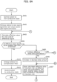
- FIG. 2 is a flowchart showing an example of an operation at the time of determining the parameters of signal processing device 1 according to the embodiment.
- Controller 100 determines the first parameter regarding the DC offset based on the output of offset adjuster 51 which is output when no signal is input to signal processing circuit 20 by subtractor 10 (step S101). Details of step S101 will be described with reference to FIG. 3 and FIG. 4 described later.
- Controller 100 determines the second parameter regarding the amplitude based on (i) an output of amplitude adjuster 52 which is output when the input signal and the feedback signal are not input to subtractor 10 and a first test signal is input to signal processing circuit 20 and (ii) the first test signal (step S102). Details of step S102 will be described with reference to FIG. 5 and FIG. 6 described later.
- Controller 100 determines a third parameter regarding the delay determined based on the difference signal in a calculator (subtractor 71) when the input signal and the feedback signal are not input to subtractor 10 and a second test signal is input to signal processing circuit 20 (step S103). Details of step S103 will be described with reference to FIG. 7 , FIG. 8A and FIG. 8B described later.
- controller 100 determines each parameter in order of, for example, the first parameter, the second parameter, and the third parameter.
- controller 100 performs a process for determining each parameter when the power of the voice reproduction device equipped with signal processing device 1 is turned on.
- controller 100 may perform the process for determining each parameter at a specific timing even after the power is turned on. This is because the circuits included in the audio reproduction device often have temperature characteristics, and the temperature rises after the power is turned on, so some cases are that the signal that is to be fed back cannot be adjusted correctly with the parameters determined when the power is turned on.
- the process of determining each parameter may be performed at a timing such as when the CD or DVD is switched after the power is turned on.
- FIG. 3 is a diagram for illustrating a signal flow at the time of determining the first parameter of signal processing device 1 according to the embodiment.
- the signal flow is indicated by a thick dashed arrow.
- FIG. 4 is a flowchart showing an example of the operation at the time of determining the first parameter of signal processing device 1 according to the embodiment.
- FIG. 4 is a flowchart showing the details of step S101 of FIG. 2 .
- Controller 100 controls switch 80 so that it is in a non-conductive state (step S201). By making switch 80 in a non-conductive state, it is possible to prevent sound from being output from speaker 130 when determining the first parameter. It should be noted that since no signal is input to signal processing circuit 20 (in other words, a no-signal is input) at the time of determining the first parameter, switch 80 may remain in the conductive state.
- Controller 100 changes the connection destination of selector 90 to no-signal generator 110 (step S202).
- the input signal is not input to subtractor 10 at the time of determining the first parameter.
- this creates a state in which no signal is input to signal processing circuit 20 by subtractor 10 (a state that a no-signal is input to signal processing circuit 20).
- controller 100 (first parameter determiner 101) determines the first parameter based on the output of offset adjuster 51 which is output when no signal is input to signal processing circuit 20 by subtractor 10.
- controller 100 first calculates the average value of the output of offset adjuster 51 at a predetermined time (the predetermined time is not particularly limited) (step S203).
- the predetermined time is not particularly limited
- the output of A/D converter 40 is ideally 0, but in fact, the output corresponds to the DC offset error of A/D converter 40.
- the first parameter is, for example, the offset amount of offset adjuster 51. In the initial state, the offset amount is, for example, 0, so the output of A/D converter 40 at this time becomes the output of offset adjuster 51 almost as it is. Since the output of A/D converter 40 may fluctuate depending on the time, the average value of the output of offset adjuster 51 in a predetermined time period is calculated.
- controller 100 determines whether the absolute value of the calculated average value is equal to or smaller than the first threshold (for example, A (positive number)) (step S204). That is, controller 100 determines whether the average value of the output of offset adjuster 51 is equal to or greater than -A and equal to or smaller than +A.
- the first threshold for example, A (positive number)
- controller 100 determines whether the average value is greater than 0 (step S205).
- controller 100 decreases the offset amount (step S206). That is, since the output of offset adjuster 51 has a value greater than A due to the DC offset error of A/D converter 40, the offset amount in offset adjuster 51 is adjusted so that the output of offset adjuster 51 approaches 0 by decreasing the offset amount of offset adjuster 51.
- controller 100 increases the offset amount (first parameter) (step S207). That is, since the output of offset adjuster 51 is smaller than -A due to the DC offset error of A/D converter 40, the offset amount in offset adjuster 51 is adjusted so that the output of offset adjuster 51 approaches 0 by increasing the offset amount of offset adjuster 51.
- step S203 the processes from step S203 are performed again. That is, it is repeated until the absolute value of the average value of the output of offset adjuster 51 becomes equal to or smaller than A that after adjusting the offset amount in offset adjuster 51, the output of offset adjuster 51 which is output when no signal is input to signal processing circuit 20 is confirmed, and according to the output, the offset amount in offset adjuster 51 is adjusted again.
- controller 100 determines the current offset amount in offset adjuster 51 as the first parameter.
- controller 100 changes the connection destination of selector 90 to compensation filter 72 (step S208), and controls switch 80 so that it is in a conductive state (step S209).
- offset adjuster 51 adjusts the DC offset for the third digital signal using the first parameter (offset amount) regarding the DC offset determined based on the output of offset adjuster 51 which is output when no signal is input to signal processing circuit 20 by subtractor 10.
- FIG. 5 is a diagram for illustrating a signal flow at the time of determining the second parameter of signal processing device 1 according to the embodiment.
- the signal flow is indicated by a thick dashed arrow.
- FIG. 6 is a flowchart showing an example of the operation at the time of determining the second parameter of signal processing device 1 according to the embodiment.
- FIG. 6 is a flowchart showing the details of step S102 of FIG. 2 .
- Controller 100 controls switch 80 so that it is in a non-conductive state (step S301). By making switch 80 in a non-conductive state, it is possible to prevent sound from being output from speaker 130 at the time of determining the second parameter. Since the first test signal is input to signal processing circuit 20 at the time of determining the second parameter, switch 80 is put into a non-conductive state so that the sound corresponding to the first test signal is not output from speaker 130.
- Controller 100 changes the connection destination of selector 90 to test signal generator 120, and causes test signal generator 120 to output a first test signal (for example, a sine wave) having a predetermined frequency (step S302).
- a first test signal for example, a sine wave
- a first test signal for example, a sine wave
- controller 100 determines the second parameter regarding the amplitude based on (i) an output of amplitude adjuster 52 which is output when the input signal and the feedback signal are not input to subtractor 10 and a first test signal is input to signal processing circuit 20 and (ii) the first test signal (the first test signal before it is signal-processed by signal processing device 1).
- controller 100 calculates the effective value for one cycle of the first test signal obtained directly from test signal generator 120 by controller 100 (step S303). It should be noted that if the effective value for one cycle of the first test signal is a fixed value and is stored in a memory or the like, the process of calculating the effective value is unnecessary.
- Controller 100 calculates the effective value for one cycle of the output of amplitude adjuster 52 (step S304). Since the first test signal input to signal processing circuit 20 is amplified by power amplification circuit 30, it is necessary to adjust the scale in order to subtract the signals before and after the amplification in subtractor 71.
- the effective value for one cycle of the first test signal obtained directly from test signal generator 120 by controller 100 corresponds to the amplitude of the signal before the amplification in power amplifier circuit 30, and the effective value for one cycle of the output of amplitude adjuster 52 corresponds to the amplitude of the signal after the amplification in power amplifier circuit 30.
- controller 100 calculates the difference obtained by subtracting the effective value for one cycle of the first test signal from the effective value for one cycle of the output of amplitude adjuster 52 (step S305).
- Controller 100 determines whether the absolute value of the calculated difference is equal to or smaller than the second threshold (for example, B (positive value)) (step S306). That is, controller 100 determines whether the difference is equal to or greater than -B and equal to or smaller than +B.
- B positive value
- controller 100 determines whether the difference is greater than 0 (step S307).
- controller 100 decreases the gain of amplitude adjuster 52 (step S308). That is, since the amplitude of the output of amplitude adjuster 52 is greater than the amplitude of the first test signal due to the amplification by power amplifier circuit 30, the gain of amplitude adjuster 52 is decreased and the difference is adjusted to approach 0.
- controller 100 increases the gain of amplitude adjuster 52 (step S309).
- step S309 the details will be described later, when the gain of amplitude adjuster 52 is made too small in step S308 and the amplitude of the output of amplitude adjuster 52 becomes smaller than the amplitude of the first test signal, the gain of amplitude adjuster 52 is increased and the difference is adjusted to approach 0.
- step S304 the processes from step S304 are performed again. That is, it is repeated until the absolute value of the difference obtained by subtracting the effective value for one cycle of the first test signal from the effective value for one cycle of the output of amplitude adjuster 52 becomes equal to or smaller than B that after adjusting the gain of amplitude adjuster 52, the output of amplitude adjuster 52 which is output when the first signal is input to signal processing circuit 20 is confirmed, and according to the output, the gain of amplitude adjuster 52 is adjusted again.
- controller 100 determines the current gain of amplitude adjuster 52 as the second parameter.
- controller 100 changes the connection destination of selector 90 to compensation filter 72 (step S310), and controls switch 80 so that it is in a conductive state (step S311).
- amplitude adjuster 52 adjusts the amplitude for the third digital signal using a second parameter regarding the amplitude determined based on (i) an output of amplitude adjuster 52 which is output when the input signal and the feedback signal are not input to subtractor 10 and a first test signal is input to signal processing circuit 20 and (ii) the first test signal.
- the second parameter may be adjusted using the maximum value of the amplitude for one cycle of the test signal.
- FIG. 7 is a diagram for illustrating a signal flow at the time of determining the third parameter of signal processing device 1 according to the embodiment.
- the signal flow is indicated by a thick dashed arrow.
- FIG. 8A and FIG. 8B are flowcharts showing an example of the operation at the time of determining the third parameter of signal processing device 1 according to the embodiment.
- FIG. 8A and FIG. 8B are flowcharts showing the details of step S103 of FIG. 2 .
- the circled "A” in FIG. 8A indicates that the next process of step S407 is step S403.
- the circled "B1" and “B2" in FIG. 8A and FIG. 8B indicate that the next process in the case of Yes in step S405 is step S408, and indicate that the next process of step S410, step S411, step S413, and step S414 is step S407.
- Controller 100 controls switch 80 so that it is in a non-conductive state (step S401). By making switch 80 in a non-conductive state, it is possible to prevent sound from being output from speaker 130 at the time of determining the third parameter. Since the second test signal is input to signal processing circuit 20 at the time of determining the third parameter, switch 80 is put into a non-conductive state so that the sound corresponding to the second test signal is not output from speaker 130.
- Controller 100 changes the connection destination of selector 90 to test signal generator 120, and causes test signal generator 120 to output a second test signal (for example, a sine wave) having a predetermined frequency (step S402).
- a second test signal for example, a sine wave
- the frequency of the second test signal and the frequency of the first test signal are different, but they may be the same frequency, or the first test signal and the second test signal may be the same signal.
- the input signal is not input to subtractor 10 at the time of determining the third parameter. With this, as shown in FIG. 7 , it becomes in such a state that the input signal and the feedback signal are not input to subtractor 10, and the second test signal is input to signal processing circuit 20. As shown in FIG.
- controller 100 determines the third parameter regarding the delay based on a difference signal which is a difference between the second digital signal having the delay adjusted by delay adjuster 53 and the third digital signal having the DC offset adjusted by offset adjuster 51 and the amplitude adjusted by amplitude adjuster 52, when the input signal and the feedback signal are not input to subtractor 10, and the second test signal is input to signal processing circuit 20.
- controller 100 calculates the effective value for one cycle of the difference signal (step S403). Since the second test signal input to signal processing circuit 20 is delayed (phase shifted) by A/D converter 40, it is also necessary to delay the signal input from signal processing circuit 20 to subtractor 71 via delay adjuster 53 or the like to the same extent in order for subtractor 71 to subtract signals at the same timing.
- Controller 100 determines whether the calculated effective value is equal to or smaller than the third threshold (for example, C (positive value)) (step S404).
- the third threshold for example, C (positive value)
- controller 100 determines whether there is an effective value of the difference signal one cycle before (step S405). Specifically, when the determination in step S405 is performed for the first time after the start of the process of determining the third parameter, there is an effective value one cycle before, and when the determination in step S405 has already been performed after the start of the process of determining the third parameter (specifically, when the process in step S407 described later has been performed), there is an effective value one cycle before.
- controller 100 increases or decreases the delay amount in delay adjuster 53 (step S406). Since it is not known whether the output of delay adjuster 53 is delayed or advanced from the output of A/D converter 40 depending on the initial value of the delay amount in delay adjuster 53, first, the delay amount in delay adjuster 53 is either increased or decreased.
- controller 100 stores the calculated effective value as an effective value one cycle before in a memory or the like, and holds in the memory or the like whether the delay amount is increased or decreased (step S407).
- the information stored in the memory or the like is used in the processes after step S403 that are performed again.
- step S403 is performed again.
- controller 100 determines whether the effective value one cycle before is stored in the memory or the like. Since the effective value one cycle before is stored in the memory or the like after the process in step S407, controller 100 determines that there is an effective value one cycle before (Yes in step S405).
- Controller 100 determines whether the effective value calculated this time is smaller than the effective value one cycle before (step S408). If the phase difference between the output of delay adjuster 53 and the output of A/D converter 40 is smaller due to the adjustment of the delay amount performed after the calculation of the effective value one cycle before, it turns out that the previous adjustment of the delay amount is the correct adjustment.
- controller 100 determines whether the delay amount was increased one cycle before (step S409).
- controller 100 further increases the delay amount (step S410) because the phase difference between the output of delay adjuster 53 and the output of A/D converter 40 is decreased by increasing the delay amount.
- controller 100 further decreases the delay amount (step S411) because the phase difference between the output of delay adjuster 53 and the output of A/D converter 40 is decreased by decreasing the delay amount.
- controller 100 decreases the delay amount (step S413) because the phase difference between the output of delay adjuster 53 and the output of A/D converter 40 is increased by increasing the delay amount.
- controller 100 increases the delay amount (step S414) because the phase difference between the output of delay adjuster 53 and the output of A/D converter 40 is increased by decreasing the delay amount.
- controller 100 determines the current delay amount in delay adjuster 53 as the third parameter.
- controller 100 changes the connection destination of selector 90 to compensation filter 72 (step S415), and controls switch 80 so that it is in a conductive state (step S416).
- delay adjuster 53 adjusts the delay of the second digital signal using the third parameter regarding the delay determined based on the difference signal when the input signal and the feedback signal are not input to subtractor 10 and the second test signal is input to signal processing circuit 20.
- the third parameter may be adjusted using the maximum value of the amplitude for one cycle of the test signal.
- controller 100 may continuously determine each parameter when determining each parameter in order of the first parameter, the second parameter, and the third parameter.
- the connection destination of selector 90 may not be changed to compensation filter 72 as shown in step S208 of FIG. 4 , and switch 80 may not be put into a conductive state as shown in step S209 of FIG. 4 .
- the connection destination of selector 90 may not be changed to compensation filter 72 as shown in step S310 of FIG. 6 , and switch 80 may not be put into a conductive state as shown in step S311 of FIG. 6 .
- amplitude adjuster 52 adjusts the amplitude of the third digital signal having the DC offset adjusted by offset adjuster 51, but the present invention is not limited thereto.
- offset adjuster 51 may adjust the DC offset for the third digital signal having the amplitude adjusted by amplitude adjuster 52. That is, the output of A/D converter 40 may be input to amplitude adjuster 52, and the output of offset adjuster 51 may be input to subtractor 71 (calculator).
- each parameter is determined in order of the first parameter, the second parameter, and the third parameter, but it is not necessary to determine in this order.
- signal processing device 1 includes switch 80, but it may not include switch 80.
- a calculator that extracts a difference signal which is a difference between the third digital signal having the DC offset adjusted by offset adjuster 51 and the amplitude adjusted by amplitude adjuster 52 and the second digital signal having the delay adjusted by delay adjuster53, and outputs the feedback signal based on the difference signal includes subtractor 71, compensation filter 72, and decimation filter 73, but is not limited thereto.
- the calculator may include at least subtractor 71.
- the present disclosure can be realized as a program for causing a computer to execute the steps included in the method according to claim 6. Furthermore, the present disclosure can be realized as a non-temporary computer-readable recording medium such as a CD-ROM on which the program is recorded.
- each step is executed by executing the program using hardware resources such as a CPU, a memory, and an input/output circuit of a computer. That is, each step is executed by the CPU obtaining data from the memory, the input/output circuit or the like and performs an operation, or outputs the operation result to the memory, the input/output circuit or the like.
- hardware resources such as a CPU, a memory, and an input/output circuit of a computer. That is, each step is executed by the CPU obtaining data from the memory, the input/output circuit or the like and performs an operation, or outputs the operation result to the memory, the input/output circuit or the like.
- the component included in signal processing device 1 of the above-described embodiment may be realized as a large scale integration (LSI) which is an integrated circuit (IC).
- LSI large scale integration
- IC integrated circuit
- the integrated circuit is not limited to the LSI, and may be realized by a dedicated circuit or a general-purpose processor.
- a programmable field programmable gate array (FPGA) or a reconfigurable processor in which the connections and settings of circuit cells inside the LSI can be reconfigured may be used.
- the components described in the attached drawings and the detailed description may include not only the components essential for problem solving but also the components not essential for problem solving. For that reason, the fact that these non-essential components are described in the accompanying drawings or detailed description should not immediately determine that those non-essential components are essential.
- the present disclosure is applicable to devices that reproduce sound of audio equipment, televisions, personal computers (PCs), mobile equipment or the like.
Landscapes
- Engineering & Computer Science (AREA)
- Power Engineering (AREA)
- Physics & Mathematics (AREA)
- Nonlinear Science (AREA)
- Multimedia (AREA)
- Acoustics & Sound (AREA)
- Signal Processing (AREA)
- Microelectronics & Electronic Packaging (AREA)
- Amplifiers (AREA)
- Circuit For Audible Band Transducer (AREA)
Claims (6)
- Signalverarbeitungsvorrichtung (1), die Folgendes umfasst:einen Subtrahierer (10), der dazu ausgelegt ist, ein Rückmeldungssignal von einem Eingangssignal zu subtrahieren, das ein digitales Audiosignal ist, und ein erstes digitales Signal auszugeben;eine Signalverarbeitungsschaltung (20), die dazu ausgelegt ist, eine Signalverarbeitung am ersten digitalen Signal durchzuführen und ein zweites digitales Signal auszugeben,eine Leistungsverstärkerschaltung (30), die dazu ausgelegt ist, das zweite digitale Signal zu verstärken, das verstärkte zweite digitale Signal in ein analoges Signal auszugeben und das analoge Signal auszugeben;einen A/D-Wandler (40), der dazu ausgelegt ist, das analoge Signal in ein drittes digitales Signal umzuwandeln und das dritte digitale Signal auszugeben;einen Versatzanpasser (51), der dazu ausgelegt ist, einen DC-Versatz für das dritte digitale Signal anzupassen;einen Amplitudenanpasser (52), der dazu ausgelegt ist, eine Amplitude für das dritte digitale Signal anzupassen;einen Verzögerungsanpasser (53), der dazu ausgelegt ist, eine Verzögerung des zweiten digitalen Signals anzupassen; undeinen Berechner, der dazu ausgelegt ist, ein Differenzsignal zu extrahieren, das eine Differenz zwischen dem dritten digitalen Signal, dessen DC-Versatz vom Versatzanpasser (51) angepasst wurde und dessen Amplitude vom Amplitudenanpasser (52) angepasst wurde, und dem zweiten digitalen Signal ist, dessen Verzögerung vom Verzögerungsanpasser (53) angepasst wurde, und das Rückmeldungssignal auf Basis des Differenzsignals auszugeben,wobei der Versatzanpasser (51) dazu ausgelegt ist, den DC-Versatz unter Verwendung eines ersten Parameters mit Bezug auf den DC-Versatz anzupassen, der auf Basis einer Ausgabe des Versatzanpassers (51) bestimmt wurde, der ausgegeben wird, wenn vom Subtrahierer (10) kein Signal in die Signalverarbeitungsschaltung (20) eingegeben wird,der Amplitudenanpasser (52) ist dazu ausgelegt, die Amplitude unter Verwendung eines zweiten Parameters mit Bezug auf die Amplitude anzupassen, der auf Basis (i) einer Ausgabe des Amplitudenanpassers (52) bestimmt wurde, der ausgegeben wird, wenn das Eingangssignal und das Rückmeldungssignal nicht in den Subtrahierer (10) eingegeben werden und ein erstes Testsignal in die Signalverarbeitungsschaltung (20) eingegeben wird, und (ii) des ersten Testsignals bestimmt wird, undder Verzögerungsanpasser (53) ist dazu ausgelegt, die Verzögerung unter Verwendung eines dritten Parameters mit Bezug auf die Verzögerung anzupassen, der auf Basis des Differenzsignals bestimmt wird, wenn das Eingangssignal und das Rückmeldungssignal nicht in den Subtrahierer (71) eingegeben werden und ein zweites Testsignal in die Signalverarbeitungsschaltung (20) eingegeben wird.
- Signalverarbeitungsvorrichtung (1) nach Anspruch 1,
wobei der Amplitudenanpasser (52) dazu ausgelegt ist, die Amplitude für das dritte digitale Signal anzupassen, dessen DC-Versatz vom Versatzanpasser (51) angepasst wurde. - Signalverarbeitungsvorrichtung (1) nach Anspruch 1 oder 2, die ferner Folgendes umfasst:eine Steuerung (100), die dazu ausgelegt ist, den ersten Parameter, den zweiten Parameter und den dritten Parameters zu bestimmen, undwobei die Steuerung (100) dazu ausgelegt ist, den ersten Parameter, den zweiten Parameter und den dritten Parameter in angegebener Reihenfolge zu bestimmen.
- Signalverarbeitungsvorrichtung (1) nach einem der Ansprüche 1 bis 3, die ferner Folgendes umfasst:
einen Schalter (80), der zwischen der Leistungsverstärkerschaltung (30) und einem Lautsprecher (130) bereitgestellt ist, der dazu ausgelegt ist, das von der Leistungsverstärkerschaltung (30) ausgegebene Analogsignal in Klang umzuwandeln. - Signalverarbeitungsvorrichtung (1) nach Anspruch 4, die ferner Folgendes umfasst:eine Steuerung (100), die dazu ausgelegt ist, den Schalter (80) zu steuern,wobei die Steuerung (100) dazu ausgelegt ist, den Schalter (80) in einen nicht leitfähigen Zustand zu bringen, wenn das erste Testsignal oder das zweite Testsignal in die Signalverarbeitungsschaltung (20) eingegeben wird.
- Verfahren zum Anpassen von Parametern für eine Signalverarbeitungsvorrichtung (1), die Folgendes beinhaltet:einen Subtrahierer (10), der ein Rückmeldungssignal von einem Eingangssignal subtrahiert, das ein digitales Audiosignal ist, und ein erstes digitales Signal ausgibt;eine Signalverarbeitungsschaltung (20), die eine Signalverarbeitung am ersten digitalen Signal durchführt und ein zweites digitales Signal ausgibt,eine Leistungsverstärkerschaltung (30), die das zweite digitale Signal verstärkt, das verstärkte zweite digitale Signal in ein analoges Signal umwandelt und das analoge Signal ausgibt;einen A/D-Wandler (40), der das analoge Signal in ein drittes digitales Signal umwandelt und das dritte digitale Signal ausgibt;einen Versatzanpasser (51), der einen DC-Versatz für das dritte digitale Signal anpasst;einen Amplitudenanpasser (52), der eine Amplitude für das dritte digitale Signal anpasst;einen Verzögerungsanpasser (53), der eine Verzögerung des zweiten digitalen Signals anpasst; undeinen Berechner, der ein Differenzsignal extrahiert, das eine Differenz zwischen dem dritten digitalen Signal, dessen DC-Versatz vom Versatzanpasser (51) angepasst wurde und dessen Amplitude vom Amplitudenanpasser (52) angepasst wurde, und dem zweiten digitalen Signal ist, dessen Verzögerung vom Verzögerungsanpasser (53) angepasst wurde, und das Rückmeldungssignal auf Basis des Differenzsignals ausgibt,wobei das Verfahren Folgendes umfasst:Bestimmen eines ersten Parameters mit Bezug auf den DC-Versatz, der auf Basis einer Ausgabe des Versatzanpassers (51) bestimmt wurde, der ausgegeben wird, wenn vom Subtrahierer (10) kein Signal in die Signalverarbeitungsschaltung (20) eingegeben wird;Bestimmen eines zweiten Parameters mit Bezug auf die Amplitude, der auf Basis (i) einer Ausgabe des Amplitudenanpassers bestimmt wurde, der ausgegeben wird, wenn das Eingangssignal und das Rückmeldungssignal nicht in den Subtrahierer (10) eingegeben werden und ein erstes Testsignal in die Signalverarbeitungsschaltung (20) eingegeben wird, und (ii) des ersten Testsignals bestimmt wird; undBestimmen eines dritten Parameters mit Bezug auf die Verzögerung auf Basis des Differenzsignals, wenn das Eingangssignal und das Rückmeldungssignal nicht in den Subtrahierer (10) eingegeben werden und ein zweites Testsignal in die Signalverarbeitungsschaltung (20) eingegeben wird.
Applications Claiming Priority (2)
| Application Number | Priority Date | Filing Date | Title |
|---|---|---|---|
| JP2019154601 | 2019-08-27 | ||
| PCT/JP2020/023507 WO2021039037A1 (ja) | 2019-08-27 | 2020-06-16 | 信号処理装置及び調整方法 |
Publications (3)
| Publication Number | Publication Date |
|---|---|
| EP4024892A1 EP4024892A1 (de) | 2022-07-06 |
| EP4024892A4 EP4024892A4 (de) | 2022-10-12 |
| EP4024892B1 true EP4024892B1 (de) | 2025-05-14 |
Family
ID=74683644
Family Applications (1)
| Application Number | Title | Priority Date | Filing Date |
|---|---|---|---|
| EP20857297.4A Active EP4024892B1 (de) | 2019-08-27 | 2020-06-16 | Signalverarbeitungsvorrichtung und einstellverfahren |
Country Status (4)
| Country | Link |
|---|---|
| US (1) | US11955935B2 (de) |
| EP (1) | EP4024892B1 (de) |
| JP (1) | JP6994656B2 (de) |
| WO (1) | WO2021039037A1 (de) |
Families Citing this family (2)
| Publication number | Priority date | Publication date | Assignee | Title |
|---|---|---|---|---|
| CN113346903B (zh) * | 2021-06-18 | 2023-07-14 | 重庆吉芯科技有限公司 | 一种在线自适应直流失调校正电路及接收机 |
| CN117336345B (zh) * | 2023-11-30 | 2024-02-23 | 苏州元脑智能科技有限公司 | 一种数据复制容灾方法、系统、装置及介质 |
Citations (5)
| Publication number | Priority date | Publication date | Assignee | Title |
|---|---|---|---|---|
| WO2001097384A2 (en) * | 2000-06-12 | 2001-12-20 | Cirrus Logic, Inc. | Real time correction of a digital pwm amplifier |
| EP1406381A1 (de) * | 2002-10-02 | 2004-04-07 | Dialog Semiconductor GmbH | Klasse-D-Verstärker mit digitaler Rückkopplung |
| JP2006121529A (ja) * | 2004-10-22 | 2006-05-11 | Pioneer Electronic Corp | D級増幅装置、増幅制御プログラム及び情報記録媒体 |
| JP2008167072A (ja) * | 2006-12-27 | 2008-07-17 | Sharp Corp | Δς変調器、および、δς変調型デジタルアナログ変換器 |
| WO2009142718A2 (en) * | 2008-05-21 | 2009-11-26 | Silicon Laboratories Inc. | Predictive feedback compensation for pwm switching amplifiers |
Family Cites Families (17)
| Publication number | Priority date | Publication date | Assignee | Title |
|---|---|---|---|---|
| JP3560398B2 (ja) * | 1995-08-31 | 2004-09-02 | 富士通株式会社 | 歪補償を有する増幅器 |
| JP3880329B2 (ja) * | 2001-04-20 | 2007-02-14 | 株式会社日立国際電気 | ループゲイン制御方法及び電力増幅回路 |
| JP3801118B2 (ja) | 2002-08-27 | 2006-07-26 | 三菱電機株式会社 | D級増幅器 |
| JP2004289424A (ja) * | 2003-03-20 | 2004-10-14 | Denon Ltd | パルス幅変調増幅装置 |
| ATE435521T1 (de) * | 2004-10-28 | 2009-07-15 | Camco Prod & Vertriebs Gmbh | Geschalteter leistungsverstärker und verfahren zur verstärkung eines digitalen signals |
| GB2419757B (en) | 2004-11-01 | 2008-11-26 | Zetex Plc | A digital amplifier |
| JP4564912B2 (ja) | 2005-10-17 | 2010-10-20 | シャープ株式会社 | 信号再生装置 |
| JP4769583B2 (ja) * | 2006-01-13 | 2011-09-07 | 株式会社日立国際電気 | 歪補償増幅装置 |
| JP5012581B2 (ja) * | 2008-03-06 | 2012-08-29 | 富士通株式会社 | 歪補償増幅装置および補正方法 |
| JP4985626B2 (ja) * | 2008-12-04 | 2012-07-25 | トヨタ自動車株式会社 | 正弦波発生装置 |
| JP5321263B2 (ja) | 2009-06-12 | 2013-10-23 | ソニー株式会社 | 信号処理装置、信号処理方法 |
| JP5383437B2 (ja) * | 2009-11-04 | 2014-01-08 | 三菱電機株式会社 | 増幅装置 |
| US9065393B2 (en) * | 2010-10-05 | 2015-06-23 | Nec Corporation | Power amplifier, radio-frequency power amplification device, and amplification control method |
| JP6286908B2 (ja) * | 2013-07-19 | 2018-03-07 | 住友電気工業株式会社 | 増幅装置及び無線通信装置 |
| JP6361030B2 (ja) | 2014-02-18 | 2018-07-25 | パナソニックIpマネジメント株式会社 | オーディオ信号増幅装置 |
| JP6340207B2 (ja) * | 2014-02-24 | 2018-06-06 | パナソニック株式会社 | 非線形歪み検出装置及び歪み補償電力増幅器 |
| JP6817567B2 (ja) * | 2017-07-21 | 2021-01-20 | パナソニックIpマネジメント株式会社 | デジタルアンプ |
-
2020
- 2020-06-16 WO PCT/JP2020/023507 patent/WO2021039037A1/ja not_active Ceased
- 2020-06-16 US US17/423,068 patent/US11955935B2/en active Active
- 2020-06-16 EP EP20857297.4A patent/EP4024892B1/de active Active
- 2020-06-16 JP JP2021504546A patent/JP6994656B2/ja active Active
Patent Citations (6)
| Publication number | Priority date | Publication date | Assignee | Title |
|---|---|---|---|---|
| WO2001097384A2 (en) * | 2000-06-12 | 2001-12-20 | Cirrus Logic, Inc. | Real time correction of a digital pwm amplifier |
| EP1374411B1 (de) * | 2000-06-12 | 2005-03-30 | Cirrus Logic Inc. | Echtzeitkorrektur eines digitalen pulsbreitenmodulatorverstärkers |
| EP1406381A1 (de) * | 2002-10-02 | 2004-04-07 | Dialog Semiconductor GmbH | Klasse-D-Verstärker mit digitaler Rückkopplung |
| JP2006121529A (ja) * | 2004-10-22 | 2006-05-11 | Pioneer Electronic Corp | D級増幅装置、増幅制御プログラム及び情報記録媒体 |
| JP2008167072A (ja) * | 2006-12-27 | 2008-07-17 | Sharp Corp | Δς変調器、および、δς変調型デジタルアナログ変換器 |
| WO2009142718A2 (en) * | 2008-05-21 | 2009-11-26 | Silicon Laboratories Inc. | Predictive feedback compensation for pwm switching amplifiers |
Also Published As
| Publication number | Publication date |
|---|---|
| US20220103138A1 (en) | 2022-03-31 |
| EP4024892A1 (de) | 2022-07-06 |
| EP4024892A4 (de) | 2022-10-12 |
| US11955935B2 (en) | 2024-04-09 |
| JPWO2021039037A1 (ja) | 2021-09-13 |
| JP6994656B2 (ja) | 2022-01-14 |
| WO2021039037A1 (ja) | 2021-03-04 |
Similar Documents
| Publication | Publication Date | Title |
|---|---|---|
| KR100750004B1 (ko) | D급 증폭기 | |
| US10110182B2 (en) | Estimating voltage on speaker terminals driven by a class-D amplifier | |
| US7538607B2 (en) | Class D amplifier | |
| EP3229371B1 (de) | Audioverstärkungssystem | |
| CN111900935B (zh) | D类放大器电路及包括其的集成电路和电子设备 | |
| EP1310041B1 (de) | Digitaler klasse-d-audioverstärker | |
| US6605991B2 (en) | Circuitry for creating a spectral null in a differential output switching amplifier and method therefor | |
| JPWO2003030373A1 (ja) | デルタシグマ変調装置及び信号増幅装置 | |
| EP4024892B1 (de) | Signalverarbeitungsvorrichtung und einstellverfahren | |
| JPWO2006087870A1 (ja) | オーディオ信号増幅回路およびそれを用いた電子機器 | |
| JP2002158549A (ja) | デジタルパワーアンプ装置 | |
| EP4262085A1 (de) | Rauschformer-fader | |
| JP4882353B2 (ja) | パルス幅変調増幅器 | |
| JP2004088431A (ja) | D級増幅器 | |
| JP2016111430A (ja) | Pwm変調装置および音声信号出力装置 | |
| US10389324B2 (en) | Audio reproduction device | |
| JP2005079692A (ja) | 信号処理装置及びd級アンプ装置 | |
| JP2001203581A (ja) | ミュート回路及び電子装置並びにそのミュート方法 | |
| JP2017175497A (ja) | Adコンバータ及びオーディオ信号増幅器 | |
| JPWO2013047550A1 (ja) | 信号合成回路、デジタルオーディオアンプ及び電源回路 | |
| JP4688225B2 (ja) | 電力増幅装置 | |
| WO2021131847A1 (ja) | 信号処理装置、増幅装置、及び再生装置 | |
| JP2008271370A (ja) | A/d変換システム | |
| JP2005117146A (ja) | 変調器 | |
| Chiu et al. | The implementation of a transient DC-link boost based digital amplifier for eliminating pulse-dropping distortion |
Legal Events
| Date | Code | Title | Description |
|---|---|---|---|
| STAA | Information on the status of an ep patent application or granted ep patent |
Free format text: STATUS: THE INTERNATIONAL PUBLICATION HAS BEEN MADE |
|
| PUAI | Public reference made under article 153(3) epc to a published international application that has entered the european phase |
Free format text: ORIGINAL CODE: 0009012 |
|
| STAA | Information on the status of an ep patent application or granted ep patent |
Free format text: STATUS: REQUEST FOR EXAMINATION WAS MADE |
|
| 17P | Request for examination filed |
Effective date: 20220121 |
|
| AK | Designated contracting states |
Kind code of ref document: A1 Designated state(s): AL AT BE BG CH CY CZ DE DK EE ES FI FR GB GR HR HU IE IS IT LI LT LU LV MC MK MT NL NO PL PT RO RS SE SI SK SM TR |
|
| A4 | Supplementary search report drawn up and despatched |
Effective date: 20220914 |
|
| RIC1 | Information provided on ipc code assigned before grant |
Ipc: H03F 3/187 20060101ALI20220908BHEP Ipc: H03F 1/30 20060101ALI20220908BHEP Ipc: H03F 3/217 20060101ALI20220908BHEP Ipc: H03F 1/32 20060101ALI20220908BHEP Ipc: H04R 3/00 20060101AFI20220908BHEP |
|
| DAV | Request for validation of the european patent (deleted) | ||
| DAX | Request for extension of the european patent (deleted) | ||
| GRAP | Despatch of communication of intention to grant a patent |
Free format text: ORIGINAL CODE: EPIDOSNIGR1 |
|
| STAA | Information on the status of an ep patent application or granted ep patent |
Free format text: STATUS: GRANT OF PATENT IS INTENDED |
|
| INTG | Intention to grant announced |
Effective date: 20240621 |
|
| GRAJ | Information related to disapproval of communication of intention to grant by the applicant or resumption of examination proceedings by the epo deleted |
Free format text: ORIGINAL CODE: EPIDOSDIGR1 |
|
| STAA | Information on the status of an ep patent application or granted ep patent |
Free format text: STATUS: REQUEST FOR EXAMINATION WAS MADE |
|
| GRAP | Despatch of communication of intention to grant a patent |
Free format text: ORIGINAL CODE: EPIDOSNIGR1 |
|
| INTC | Intention to grant announced (deleted) | ||
| STAA | Information on the status of an ep patent application or granted ep patent |
Free format text: STATUS: GRANT OF PATENT IS INTENDED |
|
| INTG | Intention to grant announced |
Effective date: 20241128 |
|
| GRAJ | Information related to disapproval of communication of intention to grant by the applicant or resumption of examination proceedings by the epo deleted |
Free format text: ORIGINAL CODE: EPIDOSDIGR1 |
|
| STAA | Information on the status of an ep patent application or granted ep patent |
Free format text: STATUS: REQUEST FOR EXAMINATION WAS MADE |
|
| GRAP | Despatch of communication of intention to grant a patent |
Free format text: ORIGINAL CODE: EPIDOSNIGR1 |
|
| STAA | Information on the status of an ep patent application or granted ep patent |
Free format text: STATUS: GRANT OF PATENT IS INTENDED |
|
| INTC | Intention to grant announced (deleted) | ||
| INTG | Intention to grant announced |
Effective date: 20250211 |
|
| GRAS | Grant fee paid |
Free format text: ORIGINAL CODE: EPIDOSNIGR3 |
|
| GRAA | (expected) grant |
Free format text: ORIGINAL CODE: 0009210 |
|
| STAA | Information on the status of an ep patent application or granted ep patent |
Free format text: STATUS: THE PATENT HAS BEEN GRANTED |
|
| AK | Designated contracting states |
Kind code of ref document: B1 Designated state(s): AL AT BE BG CH CY CZ DE DK EE ES FI FR GB GR HR HU IE IS IT LI LT LU LV MC MK MT NL NO PL PT RO RS SE SI SK SM TR |
|
| REG | Reference to a national code |
Ref country code: GB Ref legal event code: FG4D |
|
| REG | Reference to a national code |
Ref country code: CH Ref legal event code: EP |
|
| REG | Reference to a national code |
Ref country code: IE Ref legal event code: FG4D |
|
| REG | Reference to a national code |
Ref country code: DE Ref legal event code: R096 Ref document number: 602020051386 Country of ref document: DE |
|
| PGFP | Annual fee paid to national office [announced via postgrant information from national office to epo] |
Ref country code: DE Payment date: 20250618 Year of fee payment: 6 |
|
| PGFP | Annual fee paid to national office [announced via postgrant information from national office to epo] |
Ref country code: GB Payment date: 20250618 Year of fee payment: 6 |
|
| REG | Reference to a national code |
Ref country code: NL Ref legal event code: MP Effective date: 20250514 |
|
| PG25 | Lapsed in a contracting state [announced via postgrant information from national office to epo] |
Ref country code: FI Free format text: LAPSE BECAUSE OF FAILURE TO SUBMIT A TRANSLATION OF THE DESCRIPTION OR TO PAY THE FEE WITHIN THE PRESCRIBED TIME-LIMIT Effective date: 20250514 Ref country code: PT Free format text: LAPSE BECAUSE OF FAILURE TO SUBMIT A TRANSLATION OF THE DESCRIPTION OR TO PAY THE FEE WITHIN THE PRESCRIBED TIME-LIMIT Effective date: 20250915 Ref country code: ES Free format text: LAPSE BECAUSE OF FAILURE TO SUBMIT A TRANSLATION OF THE DESCRIPTION OR TO PAY THE FEE WITHIN THE PRESCRIBED TIME-LIMIT Effective date: 20250514 |
|
| REG | Reference to a national code |
Ref country code: LT Ref legal event code: MG9D |
|
| PG25 | Lapsed in a contracting state [announced via postgrant information from national office to epo] |
Ref country code: GR Free format text: LAPSE BECAUSE OF FAILURE TO SUBMIT A TRANSLATION OF THE DESCRIPTION OR TO PAY THE FEE WITHIN THE PRESCRIBED TIME-LIMIT Effective date: 20250815 Ref country code: NO Free format text: LAPSE BECAUSE OF FAILURE TO SUBMIT A TRANSLATION OF THE DESCRIPTION OR TO PAY THE FEE WITHIN THE PRESCRIBED TIME-LIMIT Effective date: 20250814 |
|
| PG25 | Lapsed in a contracting state [announced via postgrant information from national office to epo] |
Ref country code: PL Free format text: LAPSE BECAUSE OF FAILURE TO SUBMIT A TRANSLATION OF THE DESCRIPTION OR TO PAY THE FEE WITHIN THE PRESCRIBED TIME-LIMIT Effective date: 20250514 Ref country code: NL Free format text: LAPSE BECAUSE OF FAILURE TO SUBMIT A TRANSLATION OF THE DESCRIPTION OR TO PAY THE FEE WITHIN THE PRESCRIBED TIME-LIMIT Effective date: 20250514 |
|
| REG | Reference to a national code |
Ref country code: AT Ref legal event code: MK05 Ref document number: 1795834 Country of ref document: AT Kind code of ref document: T Effective date: 20250514 |
|
| PG25 | Lapsed in a contracting state [announced via postgrant information from national office to epo] |
Ref country code: BG Free format text: LAPSE BECAUSE OF FAILURE TO SUBMIT A TRANSLATION OF THE DESCRIPTION OR TO PAY THE FEE WITHIN THE PRESCRIBED TIME-LIMIT Effective date: 20250514 |
|
| PG25 | Lapsed in a contracting state [announced via postgrant information from national office to epo] |
Ref country code: HR Free format text: LAPSE BECAUSE OF FAILURE TO SUBMIT A TRANSLATION OF THE DESCRIPTION OR TO PAY THE FEE WITHIN THE PRESCRIBED TIME-LIMIT Effective date: 20250514 |
|
| PG25 | Lapsed in a contracting state [announced via postgrant information from national office to epo] |
Ref country code: AT Free format text: LAPSE BECAUSE OF FAILURE TO SUBMIT A TRANSLATION OF THE DESCRIPTION OR TO PAY THE FEE WITHIN THE PRESCRIBED TIME-LIMIT Effective date: 20250514 |
|
| PG25 | Lapsed in a contracting state [announced via postgrant information from national office to epo] |
Ref country code: RS Free format text: LAPSE BECAUSE OF FAILURE TO SUBMIT A TRANSLATION OF THE DESCRIPTION OR TO PAY THE FEE WITHIN THE PRESCRIBED TIME-LIMIT Effective date: 20250814 |
|
| PG25 | Lapsed in a contracting state [announced via postgrant information from national office to epo] |
Ref country code: IS Free format text: LAPSE BECAUSE OF FAILURE TO SUBMIT A TRANSLATION OF THE DESCRIPTION OR TO PAY THE FEE WITHIN THE PRESCRIBED TIME-LIMIT Effective date: 20250914 |
|
| PG25 | Lapsed in a contracting state [announced via postgrant information from national office to epo] |
Ref country code: LV Free format text: LAPSE BECAUSE OF FAILURE TO SUBMIT A TRANSLATION OF THE DESCRIPTION OR TO PAY THE FEE WITHIN THE PRESCRIBED TIME-LIMIT Effective date: 20250514 |
|
| PG25 | Lapsed in a contracting state [announced via postgrant information from national office to epo] |
Ref country code: SM Free format text: LAPSE BECAUSE OF FAILURE TO SUBMIT A TRANSLATION OF THE DESCRIPTION OR TO PAY THE FEE WITHIN THE PRESCRIBED TIME-LIMIT Effective date: 20250514 Ref country code: DK Free format text: LAPSE BECAUSE OF FAILURE TO SUBMIT A TRANSLATION OF THE DESCRIPTION OR TO PAY THE FEE WITHIN THE PRESCRIBED TIME-LIMIT Effective date: 20250514 |
|
| PG25 | Lapsed in a contracting state [announced via postgrant information from national office to epo] |
Ref country code: CZ Free format text: LAPSE BECAUSE OF FAILURE TO SUBMIT A TRANSLATION OF THE DESCRIPTION OR TO PAY THE FEE WITHIN THE PRESCRIBED TIME-LIMIT Effective date: 20250514 |
|
| PG25 | Lapsed in a contracting state [announced via postgrant information from national office to epo] |
Ref country code: EE Free format text: LAPSE BECAUSE OF FAILURE TO SUBMIT A TRANSLATION OF THE DESCRIPTION OR TO PAY THE FEE WITHIN THE PRESCRIBED TIME-LIMIT Effective date: 20250514 |
|
| PG25 | Lapsed in a contracting state [announced via postgrant information from national office to epo] |
Ref country code: SK Free format text: LAPSE BECAUSE OF FAILURE TO SUBMIT A TRANSLATION OF THE DESCRIPTION OR TO PAY THE FEE WITHIN THE PRESCRIBED TIME-LIMIT Effective date: 20250514 Ref country code: RO Free format text: LAPSE BECAUSE OF FAILURE TO SUBMIT A TRANSLATION OF THE DESCRIPTION OR TO PAY THE FEE WITHIN THE PRESCRIBED TIME-LIMIT Effective date: 20250514 |
|
| REG | Reference to a national code |
Ref country code: CH Ref legal event code: H13 Free format text: ST27 STATUS EVENT CODE: U-0-0-H10-H13 (AS PROVIDED BY THE NATIONAL OFFICE) Effective date: 20260127 |
|
| PG25 | Lapsed in a contracting state [announced via postgrant information from national office to epo] |
Ref country code: IT Free format text: LAPSE BECAUSE OF FAILURE TO SUBMIT A TRANSLATION OF THE DESCRIPTION OR TO PAY THE FEE WITHIN THE PRESCRIBED TIME-LIMIT Effective date: 20250514 |
|
| PG25 | Lapsed in a contracting state [announced via postgrant information from national office to epo] |
Ref country code: LU Free format text: LAPSE BECAUSE OF NON-PAYMENT OF DUE FEES Effective date: 20250616 |