EP3905334B1 - Leistungshalbleiterbauelement und herstellungsverfahren dafür - Google Patents
Leistungshalbleiterbauelement und herstellungsverfahren dafür Download PDFInfo
- Publication number
- EP3905334B1 EP3905334B1 EP19904844.8A EP19904844A EP3905334B1 EP 3905334 B1 EP3905334 B1 EP 3905334B1 EP 19904844 A EP19904844 A EP 19904844A EP 3905334 B1 EP3905334 B1 EP 3905334B1
- Authority
- EP
- European Patent Office
- Prior art keywords
- region
- conductivity
- type
- contact
- type doping
- Prior art date
- Legal status (The legal status is an assumption and is not a legal conclusion. Google has not performed a legal analysis and makes no representation as to the accuracy of the status listed.)
- Active
Links
Images




Classifications
-
- H—ELECTRICITY
- H10—SEMICONDUCTOR DEVICES; ELECTRIC SOLID-STATE DEVICES NOT OTHERWISE PROVIDED FOR
- H10D—INORGANIC ELECTRIC SEMICONDUCTOR DEVICES
- H10D84/00—Integrated devices formed in or on semiconductor substrates that comprise only semiconducting layers, e.g. on Si wafers or on GaAs-on-Si wafers
- H10D84/101—Integrated devices comprising main components and built-in components, e.g. IGBT having built-in freewheel diode
- H10D84/141—VDMOS having built-in components
- H10D84/146—VDMOS having built-in components the built-in components being Schottky barrier diodes
-
- H—ELECTRICITY
- H10—SEMICONDUCTOR DEVICES; ELECTRIC SOLID-STATE DEVICES NOT OTHERWISE PROVIDED FOR
- H10D—INORGANIC ELECTRIC SEMICONDUCTOR DEVICES
- H10D12/00—Bipolar devices controlled by the field effect, e.g. insulated-gate bipolar transistors [IGBT]
- H10D12/01—Manufacture or treatment
- H10D12/031—Manufacture or treatment of IGBTs
-
- H—ELECTRICITY
- H10—SEMICONDUCTOR DEVICES; ELECTRIC SOLID-STATE DEVICES NOT OTHERWISE PROVIDED FOR
- H10D—INORGANIC ELECTRIC SEMICONDUCTOR DEVICES
- H10D30/00—Field-effect transistors [FET]
- H10D30/01—Manufacture or treatment
- H10D30/021—Manufacture or treatment of FETs having insulated gates [IGFET]
- H10D30/028—Manufacture or treatment of FETs having insulated gates [IGFET] of double-diffused metal oxide semiconductor [DMOS] FETs
- H10D30/0291—Manufacture or treatment of FETs having insulated gates [IGFET] of double-diffused metal oxide semiconductor [DMOS] FETs of vertical DMOS [VDMOS] FETs
-
- H—ELECTRICITY
- H10—SEMICONDUCTOR DEVICES; ELECTRIC SOLID-STATE DEVICES NOT OTHERWISE PROVIDED FOR
- H10D—INORGANIC ELECTRIC SEMICONDUCTOR DEVICES
- H10D62/00—Semiconductor bodies, or regions thereof, of devices having potential barriers
- H10D62/10—Shapes, relative sizes or dispositions of the regions of the semiconductor bodies; Shapes of the semiconductor bodies
- H10D62/124—Shapes, relative sizes or dispositions of the regions of semiconductor bodies or of junctions between the regions
- H10D62/126—Top-view geometrical layouts of the regions or the junctions
-
- H—ELECTRICITY
- H10—SEMICONDUCTOR DEVICES; ELECTRIC SOLID-STATE DEVICES NOT OTHERWISE PROVIDED FOR
- H10D—INORGANIC ELECTRIC SEMICONDUCTOR DEVICES
- H10D62/00—Semiconductor bodies, or regions thereof, of devices having potential barriers
- H10D62/10—Shapes, relative sizes or dispositions of the regions of the semiconductor bodies; Shapes of the semiconductor bodies
- H10D62/17—Semiconductor regions connected to electrodes not carrying current to be rectified, amplified or switched, e.g. channel regions
- H10D62/393—Body regions of DMOS transistors or IGBTs
-
- H—ELECTRICITY
- H10—SEMICONDUCTOR DEVICES; ELECTRIC SOLID-STATE DEVICES NOT OTHERWISE PROVIDED FOR
- H10D—INORGANIC ELECTRIC SEMICONDUCTOR DEVICES
- H10D62/00—Semiconductor bodies, or regions thereof, of devices having potential barriers
- H10D62/80—Semiconductor bodies, or regions thereof, of devices having potential barriers characterised by the materials
- H10D62/83—Semiconductor bodies, or regions thereof, of devices having potential barriers characterised by the materials being Group IV materials, e.g. B-doped Si or undoped Ge
- H10D62/832—Semiconductor bodies, or regions thereof, of devices having potential barriers characterised by the materials being Group IV materials, e.g. B-doped Si or undoped Ge being Group IV materials comprising two or more elements, e.g. SiGe
- H10D62/8325—Silicon carbide
-
- H—ELECTRICITY
- H10—SEMICONDUCTOR DEVICES; ELECTRIC SOLID-STATE DEVICES NOT OTHERWISE PROVIDED FOR
- H10P—GENERIC PROCESSES OR APPARATUS FOR THE MANUFACTURE OR TREATMENT OF DEVICES COVERED BY CLASS H10
- H10P30/00—Ion implantation into wafers, substrates or parts of devices
- H10P30/20—Ion implantation into wafers, substrates or parts of devices into semiconductor materials, e.g. for doping
- H10P30/22—Ion implantation into wafers, substrates or parts of devices into semiconductor materials, e.g. for doping using masks
-
- H—ELECTRICITY
- H10—SEMICONDUCTOR DEVICES; ELECTRIC SOLID-STATE DEVICES NOT OTHERWISE PROVIDED FOR
- H10D—INORGANIC ELECTRIC SEMICONDUCTOR DEVICES
- H10D62/00—Semiconductor bodies, or regions thereof, of devices having potential barriers
- H10D62/10—Shapes, relative sizes or dispositions of the regions of the semiconductor bodies; Shapes of the semiconductor bodies
- H10D62/102—Constructional design considerations for preventing surface leakage or controlling electric field concentration
- H10D62/103—Constructional design considerations for preventing surface leakage or controlling electric field concentration for increasing or controlling the breakdown voltage of reverse-biased devices
- H10D62/105—Constructional design considerations for preventing surface leakage or controlling electric field concentration for increasing or controlling the breakdown voltage of reverse-biased devices by having particular doping profiles, shapes or arrangements of PN junctions; by having supplementary regions, e.g. junction termination extension [JTE]
- H10D62/106—Constructional design considerations for preventing surface leakage or controlling electric field concentration for increasing or controlling the breakdown voltage of reverse-biased devices by having particular doping profiles, shapes or arrangements of PN junctions; by having supplementary regions, e.g. junction termination extension [JTE] having supplementary regions doped oppositely to or in rectifying contact with regions of the semiconductor bodies, e.g. guard rings with PN or Schottky junctions
- H10D62/107—Buried supplementary regions, e.g. buried guard rings
-
- H—ELECTRICITY
- H10—SEMICONDUCTOR DEVICES; ELECTRIC SOLID-STATE DEVICES NOT OTHERWISE PROVIDED FOR
- H10D—INORGANIC ELECTRIC SEMICONDUCTOR DEVICES
- H10D64/00—Electrodes of devices having potential barriers
- H10D64/60—Electrodes characterised by their materials
- H10D64/64—Electrodes comprising a Schottky barrier to a semiconductor
-
- H—ELECTRICITY
- H10—SEMICONDUCTOR DEVICES; ELECTRIC SOLID-STATE DEVICES NOT OTHERWISE PROVIDED FOR
- H10D—INORGANIC ELECTRIC SEMICONDUCTOR DEVICES
- H10D8/00—Diodes
- H10D8/60—Schottky-barrier diodes
Definitions
- the present disclosure relates to a power semiconductor device and a manufacturing method thereof.
- Silicon carbide is one of the wide band gap semiconductor materials developed rapidly in recent decades. Compared with silicon, germanium and gallium arsenide which are widely used semiconductor materials, silicon carbide has many advantages, such as a wide band gap, a high breakdown electric field, a high carrier saturation drift rate, high thermal conductivity and high power density, and thus is an ideal material for preparing high-temperature, high-power and high-frequency devices.
- developed countries such as the United States, Europe and Japan have basically solved the problems of single-crystal growth and homoepitaxial films of silicon carbide, and occupy a leading position in the field of high-power semiconductor devices.
- a power semiconductor device includes: a substrate of a first conductivity type; a drain metal disposed on a first surface of the substrate; a drift region of the first conductivity type and disposed on a second surface of the substrate, the second surface being opposite to the first surface; a base region of a second conductivity type and disposed in the drift region; the first conductivity type and the second conductivity type being opposite conductivity types; a gate structure including a gate dielectric layer on the drift region and a gate on the gate dielectric layer, the gate structure extending above the base region; a first-conductivity-type doping region in contact with the base region on one side of the base region away from the gate structure; a source region of the first conductivity type and disposed in the base region and between the first-conductivity-type doping region and the gate structure; a contact metal disposed on the first-conductivity-type doping region and forming a contact barrier having rectification characteristics with the first-conductivity-type doping region below, wherein a dimension of the contact
- a method of manufacturing a power semiconductor device includes: acquiring a substrate provided with a drift region, the drift region being formed on one surface of the substrate, and the substrate and the drift region being of a first conductivity type; doping second-conductivity-type ions to form a base region of a second conductivity type in the drift region; the first conductivity type and the second conductivity type being opposite conductivity types; doping first-conductivity-type ions to form a first-conductivity-type doping region in the drift region that is in contact with the base region; doping the first-conductivity-type ions to form a source region of the first conductivity type in the base region; forming a contact metal on the first-conductivity-type doping region, the contact metal forming a contact barrier having rectification characteristics with the first-conductivity-type doping region below, and the contact metal extending toward the source region and above the base region not reaching the source region; forming a gate structure on the drift region, the gate structure including a gate dielectric layer on
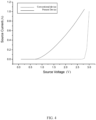
- the contact metal of the contact barrier having rectification characteristics is introduced to the bottom of the source metal, meanwhile the first-conductivity-type doping region is added below the contact metal, which replaces the parasitic body diode in the conventional power device to complete a freewheel function.
- a freewheel conduction voltage drop is obviously reduced, and a reverse recovery speed of the device is faster than that of the parasitic body diode of the conventional power device.
- a reverse recovery peak current of the improved structure is lower than that of the parasitic body diode of the conventional power device, and its reliability is higher.
- a first element, component, region, layer or portion may be referred to as a second element, component, region, layer or portion.
- Spatial relationship terms such as “under”, “underneath”, “below”, “beneath”, “over”, and “above” may be used for illustrative purposes to describe a relationship between one element or feature and another element or feature illustrated in the figures. It should be understood that, in addition to the orientations illustrated in the figures, the spatial relationship terms are intended to further include different orientations of the device in use and operation. For example, if the device in the figures is flipped, the element or feature described as “below”, “underneath” or “under” another element or feature may be oriented as “on” the another element or feature. Thus, the exemplary terms “below” and “under” may include two orientations of above and below. In addition, the device may include additional orientations (e.g., 90-degree rotation or other orientations), and thus spatial descriptors used herein may be interpreted accordingly.
- additional orientations e.g., 90-degree rotation or other orientations
- an implanted region illustrated as a rectangle typically, has rounded or curved features and/or a gradient of implant concentration at its edges rather than a binary change from an implanted region to a non-implanted region.
- a dimension of the contact metal 11 in a Y-axis direction is greater than that of the first-conductivity-type doping region 13 in the Y-axis direction, such that the contact metal 11 completely covers the first-conductivity-type doping region 13 and extends above the base region 3.
- the Y-axis direction in FIG. 1 is also a wiring direction between the gate 8 and the contact metal 11.
- the contact metal 11 is only slightly "wider" than the first-conductivity-type doping region 13, so as not to extend above the source region 4.
- the source metal 6 wraps the contact metal 11 and is in contact with the source region 4.
- the power semiconductor device further includes a body contact region 5 of the second conductivity type.
- the body contact region 5 is disposed in the base region 3 and between the source region 4 and the first-conductivity-type doping region 13, and the contact metal 11 is in contact with the body contact region 5.
- the body contact region 5 is a P+ contact region
- the contact metal 11 extends along the Y-axis direction above the body contact region 5, and the source metal 6 is also in contact with the body contact region 5.
- both sides of the gate structure are each provided with one body contact region 5, and the two body contact regions 5 are arranged in bilateral symmetry.
- the first-conductivity-type doping region 13 is also provided with mutually symmetrical body contact regions 5 on both sides thereof.
- a ratio of a dimension a of the interval between the P+ sub-doping regions in the X-axis direction to a dimension b of the P+ sub-doping regions in the X-axis direction is 0.2-0.6:1. It should be noted that the dimensions of a and b in FIG. 3 do not represent actual dimensions/proportions of the P+ sub-doping regions.
- doped ions in the second-conductivity-type doping region 12 are aluminum ions
- doped ions in the base region 3 are aluminum ions
- doped ions in the first-conductivity-type doping region 13 are nitrogen ions
- doped ions in the body contact region 5 are aluminum ions
- doped ions in the source region 4 are nitrogen ions.
Landscapes
- Electrodes Of Semiconductors (AREA)
- Metal-Oxide And Bipolar Metal-Oxide Semiconductor Integrated Circuits (AREA)
Claims (13)
- Leistungshalbleitereinrichtung, aufweisend:ein Substrat (1) von einem ersten Leitfähigkeitstyp;ein Drain-Metall (10), das auf einer ersten Oberfläche des Substrats (1) angeordnet ist;einen Drift-Bereich (2) des ersten Leitfähigkeitstyps, der auf einer zweiten Oberfläche des Substrats (1) angeordnet ist, wobei die zweite Oberfläche der ersten Oberfläche gegenüberliegt;einen Basis-Bereich (3) eines zweiten Leitfähigkeitstyps, der in dem Drift-Bereich (2) angeordnet ist; wobei der erste Leitfähigkeitstyp und der zweite Leitfähigkeitstyp entgegengesetzte Leitfähigkeitstypen sind;eine Gate-Struktur (7, 8), aufweisend einer dielektrischen Gate-Schicht (7) auf dem Drift-Bereich (2) und einem Gate (8) auf der dielektrischen Gate-Schicht (7), wobei sich die Gate-Struktur oberhalb des Basis-Bereichs (3) erstreckt;einen Dotierungsbereich (13) ersten Leitfähigkeitstyps in Kontakt mit dem Basis-Bereich (3) auf einer Seite des Basis-Bereichs (3) entfernt von der Gate-Struktur (7, 8);einen Source-Bereich (4) des ersten Leitfähigkeitstyps, der in dem Basis-Bereich (3) und zwischen dem Dotierungsbereich (13) des ersten Leitfähigkeitstyps und der Gate-Struktur (7, 8) angeordnet ist;ein Kontaktmetall (11), das auf dem Dotierungsbereich (13) des ersten Leitfähigkeitstyps angeordnet ist und mit dem darunter liegenden Dotierungsbereich (13) des ersten Leitfähigkeitstyps eine Kontaktbarriere mit Gleichrichtereigenschaften bildet, wobei eine Abmessung des Kontaktmetalls (11) in einer ersten Richtung größer ist als eine Abmessung des Dotierungsbereichs (13) des ersten Leitfähigkeitstyps in der ersten Richtung, so dass sich das Kontaktmetall (11) bis zu einer Position oberhalb des Basis-Bereichs (3) neben dem Dotierungsbereich (13) des ersten Leitfähigkeitstyps erstreckt und den Source-Bereich (4) nicht erreicht, wobei die erste Richtung eine Leitungsrichtung zwischen dem Gate (8) und dem Kontaktmetall (11) ist; undein Source-Metall (6), das das Kontaktmetall (11) umhüllt und in Kontakt mit dem Source-Bereich (4) steht;gekennzeichnet durcheinen Dotierungsbereich (12) zweiten Leitfähigkeitstyps, der in dem Drift-Bereich (2) angeordnet ist, wobei der Dotierungsbereich (12) des zweiten Leitfähigkeitstyps unter dem Basis-Bereich (3) und dem Dotierungsbereich (13) des ersten Leitfähigkeitstyps angeordnet ist und mit dem Basis-Bereich (3) und dem Dotierungsbereich (13) des ersten Leitfähigkeitstyps in Kontakt steht.
- Leistungshalbleitereinrichtung nach Anspruch 1, ferner aufweisend einen Körperkontaktbereich (5) des zweiten Leitfähigkeitstyps, der im Basis-Bereich (3) und zwischen dem Source-Bereich (4) und dem Dotierungsbereich (13) des ersten Leitfähigkeitstyps angeordnet ist, wobei das Kontaktmetall (11) in Kontakt mit dem Körperkontaktbereich (5) steht.
- Leistungshalbleitereinrichtung nach Anspruch 1, wobei der Dotierungsbereich (12) des zweiten Leitfähigkeitstyps aus einer Mehrzahl von Unterdotierungsbereichen besteht, die in Intervallen in einer zweiten Richtung verteilt sind, wobei die zweite Richtung senkrecht zu der ersten Richtung ist und eine Ebene, die durch die zweite Richtung und die erste Richtung gebildet wird, eine horizontale Ebene ist.
- Leistungshalbleitereinrichtung nach Anspruch 3, wobei die Unterdotierungsbereiche die gleiche Größe haben und in gleichen Abständen in der zweiten Richtung verteilt sind und das Verhältnis der Abmessung des Abstandes in der zweiten Richtung zu der Abmessung der Unterdotierungsbereiche in der zweiten Richtung 0,2-0,6:1 beträgt.
- Leistungshalbleitereinrichtung nach Anspruch 1, wobei ein Abmessungsverhältnis eines Teils des Dotierungsbereichs (12) vom zweiten Leitfähigkeitstyp unterhalb des Basis-Bereichs (3) zu einem Teil des Dotierungsbereichs (12) vom zweiten Leitfähigkeitstyp unterhalb des Dotierungsbereichs (13) vom ersten Leitfähigkeitstyp in der ersten Richtung 0,2-0,4:1 beträgt.
- Leistungshalbleitereinrichtung nach Anspruch 1, wobei eine Dotierungskonzentration des Dotierungsbereichs (13) des ersten Leitfähigkeitstyps größer als eine Dotierungskonzentration des Drift-Bereichs (2) und kleiner als eine Dotierungskonzentration des Source-Bereichs (4) ist.
- Leistungshalbleitereinrichtung nach Anspruch 1, wobei das Kontaktmetall (11) aus mindestens einem der folgenden Metalle hergestellt ist: Gold, Titan und Nickel.
- Leistungshalbleitereinrichtung nach Anspruch 1, wobei die Kontaktbarriere mit Gleichrichtereigenschaften eine Schottky-Barriere ist.
- Leistungshalbleitereinrichtung nach Anspruch 1, wobei der erste Leitfähigkeitstyp vom N-Typ und der zweite Leitfähigkeitstyp vom P-Typ ist.
- Leistungshalbleitereinrichtung nach einem der Ansprüche 1 bis 9, wobei die Leistungshalbleitereinrichtung eine Siliziumkarbid-Leistungshalbleitereinrichtung ist.
- Verfahren zur Herstellung einer Leistungshalbleitereinrichtung, das aufweist:Bereitstellen eines Substrats (1), das mit einem Drift-Bereich (2) versehen ist, wobei der Drift-Bereich (2) auf einer Oberfläche des Substrats (1) geformt ist und das Substrat (1) und der Drift-Bereich (2) von einem ersten Leitfähigkeitstyp sind;Dotieren von Ionen eines zweiten Leitfähigkeitstyps, um einen Basis-Bereich (3) eines zweiten Leitfähigkeitstyps in dem Drift-Bereich (2) zu formen; wobei der erste Leitfähigkeitstyp und der zweite Leitfähigkeitstyp gegenüberliegende Leitfähigkeitstypen sind;Dotieren von Ionen eines ersten Leitfähigkeitstyps, um einen Dotierungsbereich (13) eines ersten Leitfähigkeitstyps in dem Drift-Bereich (2) zu formen, der in Kontakt mit dem Basis-Bereich (3) steht;Dotieren der Ionen des ersten Leitfähigkeitstyps, um einen Source-Bereich (4) des ersten Leitfähigkeitstyps in dem Basis-Bereich (3) zu formen;Formen eines Kontaktmetalls (11) auf dem Dotierungsbereich (13) des ersten Leitfähigkeitstyps, wobei das Kontaktmetall (11) eine Kontaktbarriere mit Gleichrichtereigenschaften mit dem darunter liegenden Dotierungsbereich (13) des ersten Leitfähigkeitstyps bildet und das Kontaktmetall (11) sich in Richtung des Source-Bereichs (4) und oberhalb des Basis-Bereichs (3) erstreckt, ohne den Source-Bereich (4) zu erreichen;Formen einer Gate-Struktur (7, 8) auf dem Drift-Bereich (2), wobei die Gate-Struktur (7, 8) eine dielektrische Gate-Schicht (7) auf dem Drift-Bereich (2) und ein Gate (8) auf der dielektrischen Gate-Schicht (7) aufweist, wobei sich die Gate-Struktur (7, 8) oberhalb einer Seite des Basis-Bereichs (3) gegenüber dem Dotierungsbereich (13) vom ersten Leitfähigkeitstyp erstreckt; undFormen eines Source-Metalls (6), das das Kontaktmetall (11) umhüllt, wobei das Source-Metall (6) in Kontakt mit dem Source-Bereich (4) stehtdadurch gekennzeichnet, dassnach dem Schritt des Bereitstellens des mit dem Drift-Bereich (2) versehenen Substrats (1) und vor dem Schritt des Dotierens von Ionen des zweiten Leitfähigkeitstyps, um den Basis-Bereich (3) des zweiten Leitfähigkeitstyps im Drift-Bereich (2) zu bilden, das Verfahren ferner einen Schritt des Formens eines Dotierungsbereichs (12) des zweiten Leitfähigkeitstyps im Drift-Bereich (2) aufweist, wobei der Dotierungsbereich (12) des zweiten Leitfähigkeitstyps unter dem Basis-Bereich (3) und dem Dotierungsbereich (13) des ersten Leitfähigkeitstyps geformt wird und mit dem Basis-Bereich (3) und dem Dotierungsbereich (13) des ersten Leitfähigkeitstyps in Kontakt steht.
- Verfahren nach Anspruch 11, wobei das Verfahren nach dem Schritt des Dotierens von Ionen des zweiten Leitfähigkeitstyps zum Bilden des Basis-Bereichs (3) des zweiten Leitfähigkeitstyps im Drift-Bereich (2) und vor dem Schritt des Bildens des Kontaktmetalls (11) auf dem Dotierungsbereich (13) des ersten Leitfähigkeitstyps ferner einen Schritt des Formens eines Körperkontaktbereichs in dem Basis-Bereich (3) aufweist, wobei der Körperkontaktbereich zwischen dem Source-Bereich (4) und dem Dotierungsbereich (13) des ersten Leitfähigkeitstyps gebildet wird.
- Verfahren nach Anspruch 11, wobei der Schritt des Formens des Dotierungsbereichs (12) des zweiten Leitfähigkeitstyps im Drift-Bereich (2) aufweist: Formen des Dotierungsbereichs (12) des zweiten Leitfähigkeitstyps, der in Intervallen im Drift-Bereich (2) verteilt ist, durch Aluminiumionenimplantation mittels eines Photoresists bzw. Fotolacks als Maske und nach der Photolithographie.
Applications Claiming Priority (2)
| Application Number | Priority Date | Filing Date | Title |
|---|---|---|---|
| CN201811583692.1A CN111354794B (zh) | 2018-12-24 | 2018-12-24 | 功率半导体器件及其制造方法 |
| PCT/CN2019/127355 WO2020135313A1 (zh) | 2018-12-24 | 2019-12-23 | 功率半导体器件及其制造方法 |
Publications (4)
| Publication Number | Publication Date |
|---|---|
| EP3905334A1 EP3905334A1 (de) | 2021-11-03 |
| EP3905334A4 EP3905334A4 (de) | 2022-09-07 |
| EP3905334B1 true EP3905334B1 (de) | 2025-04-02 |
| EP3905334C0 EP3905334C0 (de) | 2025-04-02 |
Family
ID=71129209
Family Applications (1)
| Application Number | Title | Priority Date | Filing Date |
|---|---|---|---|
| EP19904844.8A Active EP3905334B1 (de) | 2018-12-24 | 2019-12-23 | Leistungshalbleiterbauelement und herstellungsverfahren dafür |
Country Status (5)
| Country | Link |
|---|---|
| US (1) | US12183818B2 (de) |
| EP (1) | EP3905334B1 (de) |
| JP (1) | JP7198931B2 (de) |
| CN (1) | CN111354794B (de) |
| WO (1) | WO2020135313A1 (de) |
Families Citing this family (2)
| Publication number | Priority date | Publication date | Assignee | Title |
|---|---|---|---|---|
| JP7707009B2 (ja) * | 2021-09-22 | 2025-07-14 | 株式会社東芝 | 半導体装置 |
| KR20230150663A (ko) * | 2022-04-22 | 2023-10-31 | 현대모비스 주식회사 | 전력 반도체 소자, 이를 포함하는 전력 반도체 칩 및 이의 제조 방법 |
Family Cites Families (32)
| Publication number | Priority date | Publication date | Assignee | Title |
|---|---|---|---|---|
| JP2003017701A (ja) * | 2001-07-04 | 2003-01-17 | Denso Corp | 半導体装置 |
| JP4860102B2 (ja) * | 2003-06-26 | 2012-01-25 | ルネサスエレクトロニクス株式会社 | 半導体装置 |
| US8704295B1 (en) * | 2008-02-14 | 2014-04-22 | Maxpower Semiconductor, Inc. | Schottky and MOSFET+Schottky structures, devices, and methods |
| US7863685B2 (en) * | 2008-05-28 | 2011-01-04 | Force-Mos Technology Corp. | Trench MOSFET with embedded junction barrier Schottky diode |
| CN102044563A (zh) | 2009-10-16 | 2011-05-04 | 上海华虹Nec电子有限公司 | Ldmos器件及其制造方法 |
| US20110156810A1 (en) | 2009-12-30 | 2011-06-30 | Intersil Americas Inc. | Integrated dmos and schottky |
| CN101853852B (zh) * | 2010-04-29 | 2011-08-17 | 苏州硅能半导体科技股份有限公司 | 单胞中集成肖特基二极管的沟槽mos器件及制造方法 |
| CN101950759A (zh) * | 2010-08-27 | 2011-01-19 | 电子科技大学 | 一种Super Junction VDMOS器件 |
| US8431470B2 (en) * | 2011-04-04 | 2013-04-30 | Alpha And Omega Semiconductor Incorporated | Approach to integrate Schottky in MOSFET |
| US9214458B2 (en) * | 2012-09-06 | 2015-12-15 | Mitsubishi Electric Corporation | Semiconductor device |
| JP2014157896A (ja) * | 2013-02-15 | 2014-08-28 | Toyota Central R&D Labs Inc | 半導体装置とその製造方法 |
| CN105074921B (zh) * | 2013-04-03 | 2017-11-21 | 三菱电机株式会社 | 半导体装置 |
| JP6244762B2 (ja) * | 2013-09-12 | 2017-12-13 | 住友電気工業株式会社 | 炭化珪素半導体装置 |
| US9214572B2 (en) * | 2013-09-20 | 2015-12-15 | Monolith Semiconductor Inc. | High voltage MOSFET devices and methods of making the devices |
| CN104617139B (zh) | 2013-11-05 | 2017-08-08 | 上海华虹宏力半导体制造有限公司 | Ldmos器件及制造方法 |
| JP6180978B2 (ja) * | 2014-03-20 | 2017-08-16 | 株式会社東芝 | 半導体装置およびその製造方法 |
| US9460926B2 (en) | 2014-06-30 | 2016-10-04 | Alpha And Omega Semiconductor Incorporated | Forming JFET and LDMOS transistor in monolithic power integrated circuit using deep diffusion regions |
| US9660074B2 (en) | 2014-08-07 | 2017-05-23 | Texas Instruments Incorporated | Methods and apparatus for LDMOS devices with cascaded RESURF implants and double buffers |
| DE112015004515B4 (de) * | 2014-10-01 | 2021-11-18 | Mitsubishi Electric Corporation | Halbleitervorrichtungen |
| KR102177431B1 (ko) | 2014-12-23 | 2020-11-11 | 주식회사 키 파운드리 | 반도체 소자 |
| US9583482B2 (en) * | 2015-02-11 | 2017-02-28 | Monolith Semiconductor Inc. | High voltage semiconductor devices and methods of making the devices |
| CN107534054B (zh) * | 2015-04-22 | 2020-08-18 | 三菱电机株式会社 | 半导体装置以及半导体装置的制造方法 |
| US10256294B2 (en) * | 2015-05-18 | 2019-04-09 | Qorvo Us, Inc. | Vertical gallium nitride power field-effect transistor with a field plate structure |
| CN105810722B (zh) | 2016-03-16 | 2019-04-30 | 中国科学院半导体研究所 | 一种碳化硅mosfet器件及其制备方法 |
| CN105762176B (zh) | 2016-04-28 | 2018-11-09 | 电子科技大学 | 碳化硅mosfet器件及其制作方法 |
| CN107425046B (zh) | 2016-05-23 | 2020-05-12 | 中芯国际集成电路制造(北京)有限公司 | 一种ldmos器件及其制作方法 |
| US20180019309A1 (en) * | 2016-07-15 | 2018-01-18 | Global Power Technologies Group, Inc. | Semiconductor device based on wideband gap semiconductor materials |
| US10707341B2 (en) * | 2016-08-25 | 2020-07-07 | Mitsubishi Electric Corporation | Semiconductor device |
| CN108257856B (zh) | 2017-12-21 | 2019-05-24 | 秦皇岛京河科学技术研究院有限公司 | 耐高温低功耗的SiC MOSFET功率器件的制备方法及其结构 |
| CN109979801B (zh) | 2017-12-28 | 2021-01-01 | 无锡华润上华科技有限公司 | 一种半导体器件的制造方法和半导体器件 |
| CN108899369B (zh) * | 2018-06-27 | 2020-11-03 | 东南大学 | 一种石墨烯沟道碳化硅功率半导体晶体管 |
| CN108807505B (zh) * | 2018-08-28 | 2021-01-08 | 电子科技大学 | 一种碳化硅mosfet器件及其制造方法 |
-
2018
- 2018-12-24 CN CN201811583692.1A patent/CN111354794B/zh active Active
-
2019
- 2019-12-23 EP EP19904844.8A patent/EP3905334B1/de active Active
- 2019-12-23 US US17/417,677 patent/US12183818B2/en active Active
- 2019-12-23 WO PCT/CN2019/127355 patent/WO2020135313A1/zh not_active Ceased
- 2019-12-23 JP JP2021536814A patent/JP7198931B2/ja active Active
Also Published As
| Publication number | Publication date |
|---|---|
| JP2022516061A (ja) | 2022-02-24 |
| JP7198931B2 (ja) | 2023-01-04 |
| US12183818B2 (en) | 2024-12-31 |
| EP3905334C0 (de) | 2025-04-02 |
| US20220115532A1 (en) | 2022-04-14 |
| WO2020135313A1 (zh) | 2020-07-02 |
| CN111354794B (zh) | 2021-11-05 |
| CN111354794A (zh) | 2020-06-30 |
| EP3905334A1 (de) | 2021-11-03 |
| EP3905334A4 (de) | 2022-09-07 |
Similar Documents
| Publication | Publication Date | Title |
|---|---|---|
| US10734514B2 (en) | Semiconductor device with trench gate structure including a gate electrode and a contact structure for a diode region | |
| US12295156B2 (en) | Semiconductor device including trench gate structure and buried shielding region and method of manufacturing | |
| JP7786512B2 (ja) | 半導体装置 | |
| US9059284B2 (en) | Semiconductor device | |
| US9209242B2 (en) | Semiconductor device with an edge termination structure having a closed vertical trench | |
| US20180197852A1 (en) | Method of Producing a Semiconductor Device | |
| US20050029558A1 (en) | High-breakdown-voltage semiconductor device | |
| US7847315B2 (en) | High efficiency rectifier | |
| US11908929B2 (en) | Semiconductor device | |
| CN114927570B (zh) | 利用新的单元几何结构增强固态功率半导体器件特性 | |
| WO2012131768A1 (ja) | 炭化珪素半導体装置およびその製造方法 | |
| US10147813B2 (en) | Tunneling field effect transistor | |
| JP3998454B2 (ja) | 電力用半導体装置 | |
| US10269952B2 (en) | Semiconductor device having steps in a termination region and manufacturing method thereof | |
| CN117878142A (zh) | 一种集成肖特基二极管的平面栅型mosfet及其制备方法 | |
| US12183818B2 (en) | Power semiconductor device and manufacturing method therefor | |
| JP4948784B2 (ja) | 半導体装置及びその製造方法 | |
| WO2015111177A1 (ja) | 半導体装置,パワーモジュール,電力変換装置,および鉄道車両 | |
| US20230326960A1 (en) | Silicon carbide semiconductor device and method of manufacturing silicon carbide semiconductor device | |
| CN108063166A (zh) | 一种沟槽结构肖特基半导体装置及其制备方法 | |
| US20250357122A1 (en) | Method of manufacturing a semiconductor device including an ohmic contact and a gate dielectric | |
| EP4668340A1 (de) | Vertikal-sperrschicht-feldeffekttransistor mit einer siliziumschicht in einer grabenstruktur | |
| CN120897485A (zh) | 一种氧化镓垂直沟槽mosfet器件及其制备方法 | |
| CN121751679A (zh) | 集成结势垒肖特基二极管的单沟道元胞结构及版图结构 | |
| HK1128361A (en) | High efficiency rectifier |
Legal Events
| Date | Code | Title | Description |
|---|---|---|---|
| STAA | Information on the status of an ep patent application or granted ep patent |
Free format text: STATUS: THE INTERNATIONAL PUBLICATION HAS BEEN MADE |
|
| PUAI | Public reference made under article 153(3) epc to a published international application that has entered the european phase |
Free format text: ORIGINAL CODE: 0009012 |
|
| STAA | Information on the status of an ep patent application or granted ep patent |
Free format text: STATUS: REQUEST FOR EXAMINATION WAS MADE |
|
| 17P | Request for examination filed |
Effective date: 20210702 |
|
| AK | Designated contracting states |
Kind code of ref document: A1 Designated state(s): AL AT BE BG CH CY CZ DE DK EE ES FI FR GB GR HR HU IE IS IT LI LT LU LV MC MK MT NL NO PL PT RO RS SE SI SK SM TR |
|
| DAV | Request for validation of the european patent (deleted) | ||
| DAX | Request for extension of the european patent (deleted) | ||
| REG | Reference to a national code |
Ref country code: DE Ref legal event code: R079 Free format text: PREVIOUS MAIN CLASS: H01L0029060000 Ipc: H01L0029100000 Ref country code: DE Ref legal event code: R079 Ref document number: 602019068252 Country of ref document: DE Free format text: PREVIOUS MAIN CLASS: H01L0029060000 Ipc: H01L0029100000 |
|
| A4 | Supplementary search report drawn up and despatched |
Effective date: 20220808 |
|
| RIC1 | Information provided on ipc code assigned before grant |
Ipc: H01L 29/06 20060101ALI20220802BHEP Ipc: H01L 21/336 20060101ALI20220802BHEP Ipc: H01L 29/78 20060101ALI20220802BHEP Ipc: H01L 29/10 20060101AFI20220802BHEP |
|
| GRAP | Despatch of communication of intention to grant a patent |
Free format text: ORIGINAL CODE: EPIDOSNIGR1 |
|
| STAA | Information on the status of an ep patent application or granted ep patent |
Free format text: STATUS: GRANT OF PATENT IS INTENDED |
|
| INTG | Intention to grant announced |
Effective date: 20240620 |
|
| GRAJ | Information related to disapproval of communication of intention to grant by the applicant or resumption of examination proceedings by the epo deleted |
Free format text: ORIGINAL CODE: EPIDOSDIGR1 |
|
| STAA | Information on the status of an ep patent application or granted ep patent |
Free format text: STATUS: REQUEST FOR EXAMINATION WAS MADE |
|
| GRAP | Despatch of communication of intention to grant a patent |
Free format text: ORIGINAL CODE: EPIDOSNIGR1 |
|
| STAA | Information on the status of an ep patent application or granted ep patent |
Free format text: STATUS: GRANT OF PATENT IS INTENDED |
|
| INTC | Intention to grant announced (deleted) | ||
| INTG | Intention to grant announced |
Effective date: 20241024 |
|
| GRAS | Grant fee paid |
Free format text: ORIGINAL CODE: EPIDOSNIGR3 |
|
| GRAA | (expected) grant |
Free format text: ORIGINAL CODE: 0009210 |
|
| STAA | Information on the status of an ep patent application or granted ep patent |
Free format text: STATUS: THE PATENT HAS BEEN GRANTED |
|
| AK | Designated contracting states |
Kind code of ref document: B1 Designated state(s): AL AT BE BG CH CY CZ DE DK EE ES FI FR GB GR HR HU IE IS IT LI LT LU LV MC MK MT NL NO PL PT RO RS SE SI SK SM TR |
|
| REG | Reference to a national code |
Ref country code: GB Ref legal event code: FG4D |
|
| REG | Reference to a national code |
Ref country code: DE Ref legal event code: R096 Ref document number: 602019068252 Country of ref document: DE |
|
| REG | Reference to a national code |
Ref country code: IE Ref legal event code: FG4D |
|
| U01 | Request for unitary effect filed |
Effective date: 20250429 |
|
| U07 | Unitary effect registered |
Designated state(s): AT BE BG DE DK EE FI FR IT LT LU LV MT NL PT RO SE SI Effective date: 20250507 |
|
| PG25 | Lapsed in a contracting state [announced via postgrant information from national office to epo] |
Ref country code: ES Free format text: LAPSE BECAUSE OF FAILURE TO SUBMIT A TRANSLATION OF THE DESCRIPTION OR TO PAY THE FEE WITHIN THE PRESCRIBED TIME-LIMIT Effective date: 20250402 |
|
| PG25 | Lapsed in a contracting state [announced via postgrant information from national office to epo] |
Ref country code: NO Free format text: LAPSE BECAUSE OF FAILURE TO SUBMIT A TRANSLATION OF THE DESCRIPTION OR TO PAY THE FEE WITHIN THE PRESCRIBED TIME-LIMIT Effective date: 20250702 Ref country code: GR Free format text: LAPSE BECAUSE OF FAILURE TO SUBMIT A TRANSLATION OF THE DESCRIPTION OR TO PAY THE FEE WITHIN THE PRESCRIBED TIME-LIMIT Effective date: 20250703 |
|
| PG25 | Lapsed in a contracting state [announced via postgrant information from national office to epo] |
Ref country code: PL Free format text: LAPSE BECAUSE OF FAILURE TO SUBMIT A TRANSLATION OF THE DESCRIPTION OR TO PAY THE FEE WITHIN THE PRESCRIBED TIME-LIMIT Effective date: 20250402 |
|
| PG25 | Lapsed in a contracting state [announced via postgrant information from national office to epo] |
Ref country code: HR Free format text: LAPSE BECAUSE OF FAILURE TO SUBMIT A TRANSLATION OF THE DESCRIPTION OR TO PAY THE FEE WITHIN THE PRESCRIBED TIME-LIMIT Effective date: 20250402 |
|
| PG25 | Lapsed in a contracting state [announced via postgrant information from national office to epo] |
Ref country code: RS Free format text: LAPSE BECAUSE OF FAILURE TO SUBMIT A TRANSLATION OF THE DESCRIPTION OR TO PAY THE FEE WITHIN THE PRESCRIBED TIME-LIMIT Effective date: 20250702 |
|
| PG25 | Lapsed in a contracting state [announced via postgrant information from national office to epo] |
Ref country code: IS Free format text: LAPSE BECAUSE OF FAILURE TO SUBMIT A TRANSLATION OF THE DESCRIPTION OR TO PAY THE FEE WITHIN THE PRESCRIBED TIME-LIMIT Effective date: 20250802 |
|
| PGFP | Annual fee paid to national office [announced via postgrant information from national office to epo] |
Ref country code: GB Payment date: 20251219 Year of fee payment: 7 |
|
| PG25 | Lapsed in a contracting state [announced via postgrant information from national office to epo] |
Ref country code: SM Free format text: LAPSE BECAUSE OF FAILURE TO SUBMIT A TRANSLATION OF THE DESCRIPTION OR TO PAY THE FEE WITHIN THE PRESCRIBED TIME-LIMIT Effective date: 20250402 |
|
| PG25 | Lapsed in a contracting state [announced via postgrant information from national office to epo] |
Ref country code: CZ Free format text: LAPSE BECAUSE OF FAILURE TO SUBMIT A TRANSLATION OF THE DESCRIPTION OR TO PAY THE FEE WITHIN THE PRESCRIBED TIME-LIMIT Effective date: 20250402 |
|
| PG25 | Lapsed in a contracting state [announced via postgrant information from national office to epo] |
Ref country code: SK Free format text: LAPSE BECAUSE OF FAILURE TO SUBMIT A TRANSLATION OF THE DESCRIPTION OR TO PAY THE FEE WITHIN THE PRESCRIBED TIME-LIMIT Effective date: 20250402 |
|
| U20 | Renewal fee for the european patent with unitary effect paid |
Year of fee payment: 7 Effective date: 20251230 |
|
| PLBE | No opposition filed within time limit |
Free format text: ORIGINAL CODE: 0009261 |
|
| STAA | Information on the status of an ep patent application or granted ep patent |
Free format text: STATUS: NO OPPOSITION FILED WITHIN TIME LIMIT |
|
| REG | Reference to a national code |
Ref country code: CH Ref legal event code: L10 Free format text: ST27 STATUS EVENT CODE: U-0-0-L10-L00 (AS PROVIDED BY THE NATIONAL OFFICE) Effective date: 20260211 |
|
| 26N | No opposition filed |
Effective date: 20260105 |