EP3796302A1 - Anzeigetafel und anzeigevorrichtung - Google Patents
Anzeigetafel und anzeigevorrichtung Download PDFInfo
- Publication number
- EP3796302A1 EP3796302A1 EP19734657.0A EP19734657A EP3796302A1 EP 3796302 A1 EP3796302 A1 EP 3796302A1 EP 19734657 A EP19734657 A EP 19734657A EP 3796302 A1 EP3796302 A1 EP 3796302A1
- Authority
- EP
- European Patent Office
- Prior art keywords
- electrode
- transistor
- capacitor
- line
- light emitting
- Prior art date
- Legal status (The legal status is an assumption and is not a legal conclusion. Google has not performed a legal analysis and makes no representation as to the accuracy of the status listed.)
- Ceased
Links
- 239000003990 capacitor Substances 0.000 claims abstract description 180
- 230000006641 stabilisation Effects 0.000 claims abstract description 73
- 238000011105 stabilization Methods 0.000 claims abstract description 73
- 239000010410 layer Substances 0.000 claims description 75
- 238000003860 storage Methods 0.000 claims description 42
- 239000000758 substrate Substances 0.000 claims description 39
- 238000009413 insulation Methods 0.000 claims description 25
- 239000004065 semiconductor Substances 0.000 claims description 15
- 239000011229 interlayer Substances 0.000 claims description 14
- 230000003071 parasitic effect Effects 0.000 claims description 13
- 230000000149 penetrating effect Effects 0.000 claims description 8
- 229910044991 metal oxide Inorganic materials 0.000 claims description 7
- 150000004706 metal oxides Chemical class 0.000 claims description 7
- 239000010409 thin film Substances 0.000 claims description 6
- OFIYHXOOOISSDN-UHFFFAOYSA-N tellanylidenegallium Chemical compound [Te]=[Ga] OFIYHXOOOISSDN-UHFFFAOYSA-N 0.000 claims description 3
- 239000000463 material Substances 0.000 description 11
- 238000000034 method Methods 0.000 description 7
- 238000010586 diagram Methods 0.000 description 6
- 239000012774 insulation material Substances 0.000 description 3
- 229910021420 polycrystalline silicon Inorganic materials 0.000 description 3
- VYPSYNLAJGMNEJ-UHFFFAOYSA-N Silicium dioxide Chemical compound O=[Si]=O VYPSYNLAJGMNEJ-UHFFFAOYSA-N 0.000 description 2
- 239000010949 copper Substances 0.000 description 2
- 238000013461 design Methods 0.000 description 2
- 239000010931 gold Substances 0.000 description 2
- 239000011777 magnesium Substances 0.000 description 2
- 238000004519 manufacturing process Methods 0.000 description 2
- 238000012986 modification Methods 0.000 description 2
- 230000004048 modification Effects 0.000 description 2
- 229920003229 poly(methyl methacrylate) Polymers 0.000 description 2
- 239000004926 polymethyl methacrylate Substances 0.000 description 2
- SMZOUWXMTYCWNB-UHFFFAOYSA-N 2-(2-methoxy-5-methylphenyl)ethanamine Chemical compound COC1=CC=C(C)C=C1CCN SMZOUWXMTYCWNB-UHFFFAOYSA-N 0.000 description 1
- NIXOWILDQLNWCW-UHFFFAOYSA-N 2-Propenoic acid Natural products OC(=O)C=C NIXOWILDQLNWCW-UHFFFAOYSA-N 0.000 description 1
- RYGMFSIKBFXOCR-UHFFFAOYSA-N Copper Chemical compound [Cu] RYGMFSIKBFXOCR-UHFFFAOYSA-N 0.000 description 1
- FYYHWMGAXLPEAU-UHFFFAOYSA-N Magnesium Chemical compound [Mg] FYYHWMGAXLPEAU-UHFFFAOYSA-N 0.000 description 1
- ZOKXTWBITQBERF-UHFFFAOYSA-N Molybdenum Chemical compound [Mo] ZOKXTWBITQBERF-UHFFFAOYSA-N 0.000 description 1
- 229910052581 Si3N4 Inorganic materials 0.000 description 1
- XUIMIQQOPSSXEZ-UHFFFAOYSA-N Silicon Chemical compound [Si] XUIMIQQOPSSXEZ-UHFFFAOYSA-N 0.000 description 1
- BQCADISMDOOEFD-UHFFFAOYSA-N Silver Chemical compound [Ag] BQCADISMDOOEFD-UHFFFAOYSA-N 0.000 description 1
- NRTOMJZYCJJWKI-UHFFFAOYSA-N Titanium nitride Chemical compound [Ti]#N NRTOMJZYCJJWKI-UHFFFAOYSA-N 0.000 description 1
- XLOMVQKBTHCTTD-UHFFFAOYSA-N Zinc monoxide Chemical compound [Zn]=O XLOMVQKBTHCTTD-UHFFFAOYSA-N 0.000 description 1
- 239000000956 alloy Substances 0.000 description 1
- 229910052782 aluminium Inorganic materials 0.000 description 1
- XAGFODPZIPBFFR-UHFFFAOYSA-N aluminium Chemical compound [Al] XAGFODPZIPBFFR-UHFFFAOYSA-N 0.000 description 1
- JYMITAMFTJDTAE-UHFFFAOYSA-N aluminum zinc oxygen(2-) Chemical compound [O-2].[Al+3].[Zn+2] JYMITAMFTJDTAE-UHFFFAOYSA-N 0.000 description 1
- 239000004020 conductor Substances 0.000 description 1
- 229910052802 copper Inorganic materials 0.000 description 1
- 238000005137 deposition process Methods 0.000 description 1
- 238000011161 development Methods 0.000 description 1
- 238000005265 energy consumption Methods 0.000 description 1
- 230000005669 field effect Effects 0.000 description 1
- 239000011521 glass Substances 0.000 description 1
- PCHJSUWPFVWCPO-UHFFFAOYSA-N gold Chemical compound [Au] PCHJSUWPFVWCPO-UHFFFAOYSA-N 0.000 description 1
- 229910052737 gold Inorganic materials 0.000 description 1
- 239000012535 impurity Substances 0.000 description 1
- AMGQUBHHOARCQH-UHFFFAOYSA-N indium;oxotin Chemical compound [In].[Sn]=O AMGQUBHHOARCQH-UHFFFAOYSA-N 0.000 description 1
- 238000005468 ion implantation Methods 0.000 description 1
- 229910052749 magnesium Inorganic materials 0.000 description 1
- 239000011159 matrix material Substances 0.000 description 1
- 229910052751 metal Inorganic materials 0.000 description 1
- 239000002184 metal Substances 0.000 description 1
- 229910021645 metal ion Inorganic materials 0.000 description 1
- 150000002739 metals Chemical class 0.000 description 1
- 229910052750 molybdenum Inorganic materials 0.000 description 1
- 239000011733 molybdenum Substances 0.000 description 1
- 229910021421 monocrystalline silicon Inorganic materials 0.000 description 1
- TWNQGVIAIRXVLR-UHFFFAOYSA-N oxo(oxoalumanyloxy)alumane Chemical compound O=[Al]O[Al]=O TWNQGVIAIRXVLR-UHFFFAOYSA-N 0.000 description 1
- 238000000059 patterning Methods 0.000 description 1
- 238000002360 preparation method Methods 0.000 description 1
- 238000011160 research Methods 0.000 description 1
- 229910052710 silicon Inorganic materials 0.000 description 1
- 239000010703 silicon Substances 0.000 description 1
- 235000012239 silicon dioxide Nutrition 0.000 description 1
- 239000000377 silicon dioxide Substances 0.000 description 1
- HQVNEWCFYHHQES-UHFFFAOYSA-N silicon nitride Chemical compound N12[Si]34N5[Si]62N3[Si]51N64 HQVNEWCFYHHQES-UHFFFAOYSA-N 0.000 description 1
- 229910052709 silver Inorganic materials 0.000 description 1
- 239000004332 silver Substances 0.000 description 1
- 239000002356 single layer Substances 0.000 description 1
- 238000006467 substitution reaction Methods 0.000 description 1
- WFKWXMTUELFFGS-UHFFFAOYSA-N tungsten Chemical compound [W] WFKWXMTUELFFGS-UHFFFAOYSA-N 0.000 description 1
- 229910052721 tungsten Inorganic materials 0.000 description 1
- 239000010937 tungsten Substances 0.000 description 1
- YVTHLONGBIQYBO-UHFFFAOYSA-N zinc indium(3+) oxygen(2-) Chemical compound [O--].[Zn++].[In+3] YVTHLONGBIQYBO-UHFFFAOYSA-N 0.000 description 1
Images

Classifications
-
- G—PHYSICS
- G09—EDUCATION; CRYPTOGRAPHY; DISPLAY; ADVERTISING; SEALS
- G09G—ARRANGEMENTS OR CIRCUITS FOR CONTROL OF INDICATING DEVICES USING STATIC MEANS TO PRESENT VARIABLE INFORMATION
- G09G3/00—Control arrangements or circuits, of interest only in connection with visual indicators other than cathode-ray tubes
- G09G3/20—Control arrangements or circuits, of interest only in connection with visual indicators other than cathode-ray tubes for presentation of an assembly of a number of characters, e.g. a page, by composing the assembly by combination of individual elements arranged in a matrix no fixed position being assigned to or needed to be assigned to the individual characters or partial characters
- G09G3/22—Control arrangements or circuits, of interest only in connection with visual indicators other than cathode-ray tubes for presentation of an assembly of a number of characters, e.g. a page, by composing the assembly by combination of individual elements arranged in a matrix no fixed position being assigned to or needed to be assigned to the individual characters or partial characters using controlled light sources
- G09G3/30—Control arrangements or circuits, of interest only in connection with visual indicators other than cathode-ray tubes for presentation of an assembly of a number of characters, e.g. a page, by composing the assembly by combination of individual elements arranged in a matrix no fixed position being assigned to or needed to be assigned to the individual characters or partial characters using controlled light sources using electroluminescent panels
- G09G3/32—Control arrangements or circuits, of interest only in connection with visual indicators other than cathode-ray tubes for presentation of an assembly of a number of characters, e.g. a page, by composing the assembly by combination of individual elements arranged in a matrix no fixed position being assigned to or needed to be assigned to the individual characters or partial characters using controlled light sources using electroluminescent panels semiconductive, e.g. using light-emitting diodes [LED]
- G09G3/3208—Control arrangements or circuits, of interest only in connection with visual indicators other than cathode-ray tubes for presentation of an assembly of a number of characters, e.g. a page, by composing the assembly by combination of individual elements arranged in a matrix no fixed position being assigned to or needed to be assigned to the individual characters or partial characters using controlled light sources using electroluminescent panels semiconductive, e.g. using light-emitting diodes [LED] organic, e.g. using organic light-emitting diodes [OLED]
- G09G3/3225—Control arrangements or circuits, of interest only in connection with visual indicators other than cathode-ray tubes for presentation of an assembly of a number of characters, e.g. a page, by composing the assembly by combination of individual elements arranged in a matrix no fixed position being assigned to or needed to be assigned to the individual characters or partial characters using controlled light sources using electroluminescent panels semiconductive, e.g. using light-emitting diodes [LED] organic, e.g. using organic light-emitting diodes [OLED] using an active matrix
- G09G3/3233—Control arrangements or circuits, of interest only in connection with visual indicators other than cathode-ray tubes for presentation of an assembly of a number of characters, e.g. a page, by composing the assembly by combination of individual elements arranged in a matrix no fixed position being assigned to or needed to be assigned to the individual characters or partial characters using controlled light sources using electroluminescent panels semiconductive, e.g. using light-emitting diodes [LED] organic, e.g. using organic light-emitting diodes [OLED] using an active matrix with pixel circuitry controlling the current through the light-emitting element
-
- G—PHYSICS
- G09—EDUCATION; CRYPTOGRAPHY; DISPLAY; ADVERTISING; SEALS
- G09G—ARRANGEMENTS OR CIRCUITS FOR CONTROL OF INDICATING DEVICES USING STATIC MEANS TO PRESENT VARIABLE INFORMATION
- G09G2300/00—Aspects of the constitution of display devices
- G09G2300/04—Structural and physical details of display devices
- G09G2300/0421—Structural details of the set of electrodes
- G09G2300/0426—Layout of electrodes and connections
-
- G—PHYSICS
- G09—EDUCATION; CRYPTOGRAPHY; DISPLAY; ADVERTISING; SEALS
- G09G—ARRANGEMENTS OR CIRCUITS FOR CONTROL OF INDICATING DEVICES USING STATIC MEANS TO PRESENT VARIABLE INFORMATION
- G09G2300/00—Aspects of the constitution of display devices
- G09G2300/08—Active matrix structure, i.e. with use of active elements, inclusive of non-linear two terminal elements, in the pixels together with light emitting or modulating elements
- G09G2300/0809—Several active elements per pixel in active matrix panels
- G09G2300/0819—Several active elements per pixel in active matrix panels used for counteracting undesired variations, e.g. feedback or autozeroing
-
- G—PHYSICS
- G09—EDUCATION; CRYPTOGRAPHY; DISPLAY; ADVERTISING; SEALS
- G09G—ARRANGEMENTS OR CIRCUITS FOR CONTROL OF INDICATING DEVICES USING STATIC MEANS TO PRESENT VARIABLE INFORMATION
- G09G2300/00—Aspects of the constitution of display devices
- G09G2300/08—Active matrix structure, i.e. with use of active elements, inclusive of non-linear two terminal elements, in the pixels together with light emitting or modulating elements
- G09G2300/0809—Several active elements per pixel in active matrix panels
- G09G2300/0842—Several active elements per pixel in active matrix panels forming a memory circuit, e.g. a dynamic memory with one capacitor
- G09G2300/0852—Several active elements per pixel in active matrix panels forming a memory circuit, e.g. a dynamic memory with one capacitor being a dynamic memory with more than one capacitor
-
- G—PHYSICS
- G09—EDUCATION; CRYPTOGRAPHY; DISPLAY; ADVERTISING; SEALS
- G09G—ARRANGEMENTS OR CIRCUITS FOR CONTROL OF INDICATING DEVICES USING STATIC MEANS TO PRESENT VARIABLE INFORMATION
- G09G2300/00—Aspects of the constitution of display devices
- G09G2300/08—Active matrix structure, i.e. with use of active elements, inclusive of non-linear two terminal elements, in the pixels together with light emitting or modulating elements
- G09G2300/0809—Several active elements per pixel in active matrix panels
- G09G2300/0842—Several active elements per pixel in active matrix panels forming a memory circuit, e.g. a dynamic memory with one capacitor
- G09G2300/0861—Several active elements per pixel in active matrix panels forming a memory circuit, e.g. a dynamic memory with one capacitor with additional control of the display period without amending the charge stored in a pixel memory, e.g. by means of additional select electrodes
-
- G—PHYSICS
- G09—EDUCATION; CRYPTOGRAPHY; DISPLAY; ADVERTISING; SEALS
- G09G—ARRANGEMENTS OR CIRCUITS FOR CONTROL OF INDICATING DEVICES USING STATIC MEANS TO PRESENT VARIABLE INFORMATION
- G09G2310/00—Command of the display device
- G09G2310/02—Addressing, scanning or driving the display screen or processing steps related thereto
- G09G2310/0243—Details of the generation of driving signals
- G09G2310/0251—Precharge or discharge of pixel before applying new pixel voltage
-
- G—PHYSICS
- G09—EDUCATION; CRYPTOGRAPHY; DISPLAY; ADVERTISING; SEALS
- G09G—ARRANGEMENTS OR CIRCUITS FOR CONTROL OF INDICATING DEVICES USING STATIC MEANS TO PRESENT VARIABLE INFORMATION
- G09G2320/00—Control of display operating conditions
- G09G2320/02—Improving the quality of display appearance
- G09G2320/0209—Crosstalk reduction, i.e. to reduce direct or indirect influences of signals directed to a certain pixel of the displayed image on other pixels of said image, inclusive of influences affecting pixels in different frames or fields or sub-images which constitute a same image, e.g. left and right images of a stereoscopic display
- G09G2320/0214—Crosstalk reduction, i.e. to reduce direct or indirect influences of signals directed to a certain pixel of the displayed image on other pixels of said image, inclusive of influences affecting pixels in different frames or fields or sub-images which constitute a same image, e.g. left and right images of a stereoscopic display with crosstalk due to leakage current of pixel switch in active matrix panels
-
- G—PHYSICS
- G09—EDUCATION; CRYPTOGRAPHY; DISPLAY; ADVERTISING; SEALS
- G09G—ARRANGEMENTS OR CIRCUITS FOR CONTROL OF INDICATING DEVICES USING STATIC MEANS TO PRESENT VARIABLE INFORMATION
- G09G2320/00—Control of display operating conditions
- G09G2320/02—Improving the quality of display appearance
- G09G2320/0219—Reducing feedthrough effects in active matrix panels, i.e. voltage changes on the scan electrode influencing the pixel voltage due to capacitive coupling
-
- G—PHYSICS
- G09—EDUCATION; CRYPTOGRAPHY; DISPLAY; ADVERTISING; SEALS
- G09G—ARRANGEMENTS OR CIRCUITS FOR CONTROL OF INDICATING DEVICES USING STATIC MEANS TO PRESENT VARIABLE INFORMATION
- G09G2320/00—Control of display operating conditions
- G09G2320/04—Maintaining the quality of display appearance
- G09G2320/043—Preventing or counteracting the effects of ageing
Definitions
- Embodiments of the present disclosure relate to a display panel and a display device.
- organic light emitting diode (OLED) display panels have characteristics of self-luminous, high contrast, low energy consumption, wide viewing angle, fast response, applicable for flexible panels, wide operating temperature range and simple manufacturing, and have broad development prospects.
- Embodiments of the present disclosure provide a display panel and a display device.
- An embodiment of the present disclosure provides a display panel, which includes a pixel circuit structure, a data line and a voltage signal line, wherein the data line is connected to the pixel circuit structure to provide a data signal; the voltage signal line is connected to the pixel circuit structure to provide a voltage signal, the voltage signal is a constant voltage signal; the pixel circuit structure includes a first stabilization capacitor provided between the data line and the voltage signal line.
- the display panel further includes a gate line and a light emitting element.
- the gate line is connected to the pixel circuit structure to provide a scan signal;
- the pixel circuit structure further includes a driving transistor, the driving transistor is electrically connected to the light emitting element and outputs a driving current to drive the light emitting element to emit light under control of the scan signal and the data signal.
- a capacitance value of the first stabilization capacitor is equal to or greater than 10 times of a capacitance value of a parasitic capacitance between the data line and a gate electrode of the driving transistor.
- the first stabilization capacitor includes a first capacitor electrode and a second capacitor electrode, the first capacitor electrode is electrically connected to the voltage signal line, and the second capacitor electrode is electrically connected to the data line.
- the display panel further includes a substrate.
- the pixel circuit structure, the gate line, the data line and the voltage signal line are on the substrate, the first capacitor electrode and the second capacitor electrode overlap with each other in a direction perpendicular to the substrate.
- the voltage signal line and the data line are disposed in a same layer and extend in a same direction, the first capacitor electrode is located on a side of the data line close to the substrate; the display panel further includes an interlayer insulation layer between the data line and the first capacitor electrode, the first capacitor electrode is connected to the voltage signal line through a via hole penetrating through the interlayer insulation layer.
- the display panel further includes a compensation transistor.
- a first electrode and a second electrode of the driving transistor are respectively connected to the voltage signal line and the light emitting element; a first electrode and a second electrode of the compensation transistor are respectively connected to the second electrode and a gate electrode of the driving transistor, and a gate electrode of the compensation transistor is connected to the gate line.
- the compensation transistor includes an active layer, the active layer includes a first electrode region, a second electrode region, and a channel region between the first electrode region and the second electrode region, the first electrode region and the second electrode region are conductive regions, the display panel further includes a first connecting electrode, the first connecting electrode connects the second electrode region and the gate electrode of the driving transistor.
- the pixel circuit structure further includes a storage capacitor, a first electrode and a second electrode of the storage capacitor are electrically connected to the voltage signal line and the gate electrode of the driving transistor, respectively; the first electrode of the storage capacitor is disposed in the same layer as the first capacitor electrode, and overlaps with the gate electrode of the driving transistor in the direction perpendicular to the substrate.
- the first electrode of the storage capacitor and the data line overlap with each other in the direction perpendicular to the substrate.
- the first electrode of the storage capacitor is provided with an opening, and the first connecting electrode is electrically connected to the gate electrode of the driving transistor through the opening.
- the pixel circuit structure further includes a second stabilization capacitor, the second stabilization capacitor is located between the data line and the first electrode of the driving transistor, or the second stabilization capacitor is located between the voltage signal line and the first electrode of the driving transistor; or, the pixel circuit structure further includes a second stabilization capacitor and a third stabilization capacitor, one of the second stabilization capacitor and the third stabilization capacitor is located between the data line and the first electrode of the driving transistor, and the other of the second stabilization capacitor and the third stabilization capacitor is located between the voltage signal line and the first electrode of the driving transistor.
- the display panel further includes a light emitting control signal line, a reset control signal line and an initialization signal line
- the pixel circuit structure further includes a data writing transistor, a first light emitting control transistor, a second light emitting control transistor, a first reset transistor and a second reset transistor, wherein a first electrode and a second electrode of the data writing transistor are electrically connected to the data line and the first electrode of the driving transistor, respectively, and a gate electrode of the data writing transistor is electrically connected to the gate line;
- a gate electrode of the first light emitting control transistor is electrically connected to the light emitting control signal line, a first electrode and a second electrode of the first light emitting control transistor are electrically connected to the voltage signal line and the first electrode of the driving transistor, respectively;
- a gate electrode of the second light emitting control transistor is electrically connected to the light emitting control signal line, a first electrode and a second electrode of the second light emitting control transistor are electrically connected to the second electrode of the driving transistor and the first electrode of the light emitting
- the voltage signal line includes a power line.
- An embodiment of the present disclosure also provides a display panel, which includes a substrate, and a pixel circuit structure, a light emitting element, a gate line, a data line, a first power line, a second power line, a light emitting control signal line, an initialization signal line and a reset control signal line on the substrate, the pixel circuit structure including a storage capacitor, a driving transistor, a data writing transistor, a compensation transistor, a first light emitting control transistor, a second light emitting control transistor, a first reset transistor and a second reset transistor, wherein a first electrode of the storage capacitor is electrically connected to the first power line, a second electrode of the storage capacitor is electrically connected to a second electrode of the compensation transistor through a first connecting electrode; a gate electrode of the data writing transistor is electrically connected to the gate line, a first electrode and a second electrode of the data writing transistor are electrically connected to the data line and a first electrode of the driving transistor, respectively; a gate electrode of the compensation transistor is electrically connected to the gate line
- the gate line, the gate electrode of the driving transistor and the second electrode of the storage transistor are disposed in a same layer; the first capacitor electrode, the initialization signal line and the first electrode of the storage transistor are disposed in a same layer; the data line, the first power line and the first connecting electrode are disposed in a same layer; the first capacitor electrode and the data line overlap with each other in a direction perpendicular to the substrate.
- the compensation transistor and the first reset transistor are metal oxide semiconductor thin film transistors or double gate thin film transistors.
- the first capacitor electrode is electrically connected to the first power line
- the first stabilization capacitor further includes a second capacitor electrode
- the second capacitor electrode is electrically connected to the data line
- the first capacitor electrode and the second capacitor electrode overlap with each other in a direction perpendicular to the substrate.
- the first capacitor electrode is located on a side of the data line close to the substrate; the display panel further includes an interlayer insulation layer between the data line and the first capacitor electrode, the first capacitor electrode is connected to the first power line through a via hole penetrating through the interlayer insulation layer.
- the first electrode of the storage capacitor and the gate electrode of the driving transistor overlap with each other in a direction perpendicular to the substrate; the first electrode of the storage capacitor and the data line overlap with each other in the direction perpendicular to the substrate; an opening is disposed in the first electrode of the storage capacitor, and the first connecting electrode is electrically connected to the gate electrode of the driving transistor through the opening.
- the pixel circuit structure further includes a second stabilization capacitor, the second stabilization capacitor is located between the data line and the first electrode of the driving transistor, or the second stabilization capacitor is located between the first power line and the first electrode of the driving transistor; or, the pixel circuit structure further includes a second stabilization capacitor and a third stabilization capacitor, one of the second stabilization capacitor and the third stabilization capacitor is located between the data line and the first electrode of the driving transistor, and the other of the second stabilization capacitor and the third stabilization capacitor is located between the first power line and the first electrode of the driving transistor.
- An embodiment of the present disclosure also provides a display device, which includes the display panel mentioned above.
- a driving transistor is connected to an organic light emitting element, and outputs a driving current to the organic light emitting element under the control of signals such as a data signal and a scan signal, thereby driving the organic light emitting element to emit light. Because the magnitude of a gate voltage of the driving transistor is directly related to the magnitude of the driving current of the organic light emitting element, the stabilization of the gate signal is an important factor for achieving stable light emission of the organic light emitting element and stable display of the display panel.
- an inventor of the present application has found that when the data signal is transmitted on the data line, the fluctuation of the data signal easily interferes with the gate signal of the driving transistor.
- the data signal interferes with the gate signal through a parasitic capacitance formed between the data line and the gate electrode of the driving transistor, thereby affecting the stability of the gate signal.
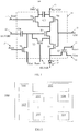
- FIG. 1 is a schematic structural diagram of a display panel provided by an embodiment of the present disclosure
- FIG. 2 is a schematic plan view of a display panel provided by an embodiment of the present disclosure.
- the display panel 100 includes a plurality of pixel units 101 arranged in a matrix, and each of the plurality of pixel units 101 includes a pixel circuit structure 10, a light emitting element 20, a gate line 11, a data line 12, and a voltage signal line.
- the light emitting element 20 is an organic light emitting element OLED, and the light emitting element 20 emits red light, green light, blue light, or white light, etc., when driven by a corresponding pixel circuit structure 10 thereof.
- the voltage signal line can be one or more.
- the voltage signal line can include signal lines that provide a constant voltage signal, such as a first power line 13, a second power line 14, and an initialization signal line 16, etc..
- the first power line 13 is configured to provide a constant first voltage signal ELVDD to the pixel circuit structure 10
- the second power line 14 is configured to provide a constant second voltage signal ELVSS
- the first voltage signal ELVDD is greater than the second voltage signal ELVSS.
- the light emitting control signal line 15 is configured to provide a light emitting control signal EM.
- the initialization signal line 16 and a reset control signal line 17 are respectively configured to provide an initialization signal Vint and a reset control signal Reset.
- the initialization signal Vint is a constant voltage signal, the magnitude of which can be, for example, between the first voltage signal ELVDD and the second voltage signal ELVSS, but is not limited thereto.
- the initialization signal Vint can also be less than or equal to the second voltage signal ELVSS.
- the pixel circuit structure 10 includes a driving transistor T1, a data writing transistor T2, a compensation transistor T3, a first light emitting control transistor T4, a second light emitting control transistor T5, a first reset transistor T6, a second reset transistor T7, and a storage capacitor Cst.
- the driving transistor T1 is electrically connected to the light emitting element 20, and outputs a driving current, under the control of signals such as the scan signal Scan, the data signal Data, the first voltage signal ELVDD, and the second voltage signal ELVSS, etc., to drive the light emitting element 20 to emit light.
- the pixel circuit structure 10 further includes a first stabilization capacitor C1 between the data line 12 and the voltage signal line, and the voltage signal line shown in FIG. 1 refers to the first power line 13.
- the first stabilization capacitor C1 can reduce the interference of the parasitic capacitance between the data line 12 and the gate electrode of the driving transistor T1 to the gate signal of the driving transistor T1.
- a capacitance value of the first stabilization capacitor C1 can be designed to be equal to or greater than 10 times of the parasitic capacitance between the data line 12 and the gate electrode of the driving transistor T1.
- the capacitance value of the parasitic capacitance can be neglected compared with that of the first stabilization capacitor C1, the influence of the data line signal on the gate signal through the parasitic capacitance is also negligible.
- the first stabilization capacitor C1 can be arranged in a variety of ways.
- the first stabilization capacitor can include a first capacitor electrode and a second capacitor electrode, the first capacitor electrode is electrically connected to the first power source line 13, and the second capacitor electrode is electrically connected to the data line 12.
- the first capacitor electrode can be a part of the first power line 13 or an electrode that is separately provided and electrically connected to the first power line 13, both of which are included in the scope of "the first capacitor electrode is electrically connected to the first power source line” mentioned above.
- the second capacitor electrode can be a part of the data line 12 or an electrode that is separately provided and electrically connected to the data line 12, both of which are included in the scope of "the second capacitor electrode is electrically connected to the data line” mentioned above.
- a pixel circuit structure is prepared on a substrate of the display panel 100 by semiconductor techniques, and the pixel circuit structure includes a circuit layer, an insulation layer and the like that are stacked.
- the first capacitor electrode and the second capacitor electrode can overlap with each other in a direction perpendicular to the substrate of the display panel 100, and are spaced apart from each other by the insulation layer (a dielectric layer), thereby forming a capacitor.
- the capacitance value of the first stabilization capacitor C1 can be adjusted by designing a distance between the first capacitor electrode and the second capacitor electrode, a material of the intermediate insulation layer (i.e., a dielectric constant), and an overlapping area between the first capacitor electrode and the second capacitor electrode.
- a first electrode of the storage capacitor Cst is electrically connected to the first power line 13, and a second electrode of the storage capacitor Cst is electrically connected to a second electrode of the compensation transistor T3.
- a gate electrode of the data writing transistor T2 is electrically connected to the gate line 11, a first electrode and a second electrode of the data writing transistor T2 are electrically connected to the data line 12 and a first electrode of the driving transistor T1, respectively.
- a gate electrode of the compensation transistor T3 is electrically connected to the gate line 11, the first electrode and a second electrode of the compensation transistor T3 are electrically connected to a second electrode and a gate electrode of the driving transistor T1, respectively.
- a gate electrode of the first light emitting control transistor T4 is electrically connected to the light emitting control signal line 15, a first electrode and a second electrode of the first light emitting control transistor T4 are electrically connected to the first power line 13 and the first electrode of the driving transistor T1, respectively.
- a gate electrode of the second light emitting control transistor T5 is electrically connected to the light emitting control signal line 15, a first electrode and a second electrode of the second light emitting control transistor T5 are electrically connected to the second electrode of the driving transistor T1 and a first electrode of the light emitting element 20, respectively.
- a gate electrode of the first reset transistor T6 is electrically connected to the reset control signal line 17, a first electrode and a second electrode of the first reset transistor T6 are electrically connected to the initialization signal line 16 and the gate electrode of the driving transistor T1, respectively.
- a gate electrode of the second reset transistor T7 is electrically connected to the reset control signal line 17, a first electrode and a second electrode of the second reset transistor T7 are electrically connected to the initialization signal line 16 and the first electrode of the light emitting element 20, respectively.
- a second electrode of the light emitting element 20 is electrically connected to the second power line 14.
- a source electrode and a drain electrode of a transistor used here can be symmetrical in structure, so that the source electrode and the drain electrode can be indistinguishable in structure.
- one of the two electrodes is directly described as a first electrode while the other of the two electrodes is directly described as a second electrode, so the first and second electrodes of all or a part of the transistors in the embodiments of the present disclosure are interchangeable as needed.
- the first electrode of the transistors in the embodiments of the present disclosure can be a source electrode, and the second electrode thereof can be a drain electrode; alternatively, the first electrode of the transistors is a drain electrode, and the second electrode thereof is a source electrode.
- the transistors can be divided into N-type and P-type transistors according to the characteristics of the transistors.
- the embodiments of the present disclosure are described by taking a case that the transistors are P-type transistors as an example. Based on the description and teaching of the implementations of the present disclosure, those skilled in the art can easily imagine that at least some of the transistors in the pixel circuit structure of the embodiments of the present disclosure can adopt an implementation of adopting a N-type transistor, that is, an implementation adopting N-type transistors or adopting a combination of N-type transistors and P-type transistors. Therefore, these implementations are also within the protection scope of the present disclosure.
- an active layer of the transistors adopted in the embodiments of the present disclosure can be made of mono-crystalline silicon, poly-crystalline silicon (e.g., low temperature poly-crystalline silicon), or a metal oxide semiconductor material (e.g., IGZO, AZO, etc.).
- the transistors are all P-type LTPS (low temperature poly-crystalline silicon) thin film transistors.
- the compensation transistor T3 (threshold compensation transistor) and the first reset transistor T6 that are directly connected to the gate electrode of the driving transistor T1 are metal oxide semiconductor thin film transistors, that is, a channel material of these transistors is a metal oxide semiconductor material (such as IGZO, AZO, etc.).
- the metal oxide semiconductor thin film transistors have a low leakage current, which can help reduce the gate leakage current of the driving transistor T1.
- the transistors adopted in the embodiments of the present disclosure can include various structures, such as a top gate type, a bottom gate type, or a double gate structure.
- the compensation transistor T3 and the first reset transistor T6 that are directly connected to the gate electrode of the driving transistor T1 are double gate thin film transistors, which can help reduce the gate leakage current of the driving transistor T1.
- the display panel 100 provided by the embodiment of the present disclosure further includes: a data driver 102, a scan driver 103, and a controller 104.
- the data driver 102 is configured to provide a data signal Data to the pixel unit 101 according to an instruction of the controller 104;
- the scan driver 103 is configured to provide a light emitting control signal EM, a scan signal Scan, and a reset control signal Reset, etc., to the pixel unit 101 according to an instruction of the controller 104.
- the scan driver 103 is a GOA (Gate On Array) structure mounted on the display panel, or a driver chip (IC) structure bonding to the display panel.
- GOA Gate On Array
- the display panel 100 further includes a power source (not shown in FIG. 2 ) for providing the above voltage signal, which can be a voltage source or a current source as needed, and the power source is configured to supply the pixel unit 101 with the first power voltage ELVDD, the second power voltage ELVSS, and the initialization signal Vint, etc., through the first power line 13, the second power line 14, and the initialization signal line 16, respectively.
- a power source (not shown in FIG. 2 ) for providing the above voltage signal, which can be a voltage source or a current source as needed, and the power source is configured to supply the pixel unit 101 with the first power voltage ELVDD, the second power voltage ELVSS, and the initialization signal Vint, etc., through the first power line 13, the second power line 14, and the initialization signal line 16, respectively.
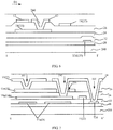
- FIG. 3 is a timing signal diagram of a pixel unit in a display panel provided by an embodiment of the present disclosure. A driving method of a pixel unit in the display panel provided by the embodiment of the present disclosure will be described below with reference to FIG. 3 .
- the driving method of the pixel unit includes a reset phase t1, a data writing and threshold compensating phase t2, and a light emitting phase t3.
- the light emitting control signal EM is set to be a turn-off voltage
- the reset control signal Reset is set to be a turn-on voltage
- the scan signal Scan is set to be a turn-off voltage.
- the light emitting control signal EM is set to be a turn-off voltage
- the reset control signal Reset is set to be a turn-off voltage
- the scan signal Scan is set to be a turn-on voltage.
- the light emitting control signal EM is set to be a turn-on voltage
- the reset control signal Reset is set to be a turn-off voltage
- the scan signal Scan is set to be a turn-off voltage.
- the turn-on voltage refers to a voltage that enables the first electrode and the second electrode of the respective transistors to be turned on
- the turn-off voltage refers to a voltage that enables the first electrode and the second electrode of the respective transistors to be turned off.
- the turn-on voltage is a low voltage (for example, 0V)
- the turn-off voltage is a high voltage (for example, 5V)
- the transistor is an N-type transistor
- the turn-on voltage is a high voltage (for example, 5V)
- the turned-off voltage is a low voltage (for example, 0V).
- the driving waveforms shown in FIG. 3 are all described by taking P-type transistors as an example, that is, the turn-on voltage is a low voltage (for example, 0 V), and the turn-off voltage is a high voltage (for example, 5 V).
- the light emitting control signal EM is the turn-off voltage
- the reset control signal Reset is the turn-on voltage
- the scan signal Scan is the turn-off voltage.
- the first reset transistor T6 and the second reset transistor T7 are in a turn-on state
- the data writing transistor T2, the compensation transistor T3, the first light emitting control transistor T4, and the second light emitting control transistor T5 are in a turn-off state.
- the initialization signal (initialization voltage) Vint is transmitted to the gate electrode of the driving transistor T1 through the first reset transistor T6, and is stored by the storage capacitor Cst, so as to reset the driving transistor T1 and eliminate data stored during a previous light emitting (a previous frame); the initialization signal Vint is transmitted to the first electrode of the light emitting element 20 through the second reset transistor T7, so as to reset the light emitting element 20.
- the light emitting control signal EM is the turn-off voltage
- the reset control signal Reset is the turn-off voltage
- the scan signal Scan is the turn-on voltage.
- the data writing transistor T2 transmits the data signal voltage Vdata to the first electrode of the driving transistor T1, that is, the data writing transistor T2 receives the scan signal Scan and the data signal Data, and writes the data signal Data to the first electrode of the driving transistor T1 according to the scan signal Scan.
- the compensation transistor T3 is turned on to connect the driving transistor T1 into a diode structure, whereby the gate electrode of the driving transistor T1 can be charged.
- the gate voltage of the driving transistor T1 is Vdata + Vth, where Vdata is the data signal voltage, and Vth is the threshold voltage of the driving transistor T1.
- the compensation transistor T3 receives the scan signal Scan and performs threshold voltage compensation on the gate voltage of the driving transistor T1 according to the scan signal Scan.
- the voltage difference between two terminals of the storage capacitor Cst is ELVDD-Vdata-Vth.
- the light emitting control signal EM is the turn-on voltage
- the reset control signal Reset is the turn-off voltage
- the scan signal Scan is the turn-off voltage.
- the first light emitting control transistor T4 and the second light emitting control transistor T5 are in a turn-on state, while the data writing transistor T2, the compensation transistor T3, the first reset transistor T6, and the second reset transistor T7 arc in a turn-off state.
- the first power signal ELVDD is transmitted to the first electrode of the driving transistor T1 through the first light emitting control transistor T4, the gate voltage of the driving transistor T1 is maintained at Vdata + Vth, and the driving current I flows into the light emitting element 20 through the first light emitting control transistor T4, the driving transistor T1 and the second light emitting control transistor T5, and the light emitting element 20 emits light. That is, the first light emitting control transistor T4 and the second light emitting control transistor T5 receive the light emitting control signal EM, and control the light emitting element 20 to emit light according to the light emitting control signal EM.
- the current flowing through the light emitting element 20 is independent of the threshold voltage of the driving transistor T1. Therefore, the pixel circuit structure compensates for the threshold voltage of the driving transistor T1 very well.
- the reset control signal line 17 can be set as a gate line of a previous row of pixel units, that is, the reset control signal is served by a scan signal Scan(n-1) of the previous row of pixel units, thereby reducing wiring and the number of signals.
- the ratio of the duration of the light emitting phase t3 to the display period of one frame can be adjusted.
- the luminous brightness can be controlled by adjusting the ratio of the duration of the light emitting phase t3 to the display period of one frame.
- the scan driver 103 in the display panel or a driver additionally provided the ratio of the duration of the light emitting phase t3 to the display period of one frame can be adjusted.
- the first stabilization capacitor C1 can also be located between the data line 12 and another signal line that provides a constant voltage signal.
- the first stabilization capacitor C1 is located between the data line 12 and the second power line 14, or the first stabilization capacitor C1 is located between the data line 12 and the initialization signal line 16.
- the first light emitting control transistor T4 or the second light emitting control transistor T5 may not be provided, or, the first reset transistor T6 or the second reset transistor T7 may not be provided. That is, the embodiment of the present disclosure is not limited to the specific pixel circuit shown in FIG. 1 , and other pixel circuits that enable compensation for the driving transistor can be adopted. Based on the description and teaching of the implementation of the present disclosure, other arrangements that can be easily conceived by those skilled in the art without creative efforts are within the protection scope of the present disclosure.
- FIG. 4 is a schematic diagram of a display panel provided by another embodiment of the present disclosure.
- the display panel provided by the present embodiment differs from the display panel in FIG. 1
- the display panel 100 further includes a second stabilization capacitor C2 and/or a third stabilization capacitor C3.
- the second stabilization capacitor C2 is located between the data line 12 and the first electrode of the driving transistor T1
- the third stabilization capacitor C3 is located between the first power source line 13 and the first electrode of the driving transistor T1. Because the presence of the second stabilization capacitor C2, the interference of the parasitic capacitance between the data line 12 and the gate electrode of the driving transistor T1 to the gate signal of the driving transistor T1 can be further reduced. Because the presence of the third stabilization capacitor C3, the interference of the parasitic capacitance between the first power line 13 and the gate electrode of the driving transistor T1 to the gate signal of the driving transistor T1 can be further reduced.
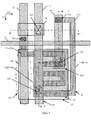
- FIG. 5 is a schematic plan view (exemplary layout) of the display panel 100 of FIG. 1 .
- the driving transistor T1, the data writing transistor T2, the compensation transistor T3, the storage capacitor Cst and the first stabilization capacitor C1 is shown, and the structures of other transistors are not shown.
- FIG. 6 is a cross-sectional view of the display panel shown in FIG. 5 taken along section line I-I'
- FIG. 7 is a cross-sectional view of the display panel shown in FIG. 5 taken along section line II-II'.
- the display panel 100 provided by the embodiment of the present disclosure will be exemplarily described below with reference to FIGS. 5-7 .
- disposed in the same layer refers to that two (or more than two) material layer structures are formed by the same deposition process and patterned by the same patterning process, so the two (more than two) have the same material.
- an electrical connection between A and B as illustrated in the present disclosure includes a case where A is a part of B and a case where B is a part of A.
- T1g, T1s, T1d and T1a are used to represent the gate electrode, the first electrode, the second electrode, and the channel region of the driving transistor T1, respectively;
- T2g, T2s, T2d and T2a are used to represent the gate electrode, the first electrode, the second electrode, and the channel region of the data writing transistor T2, respectively;
- T3g, T3s, T3d and T3a are used to represent the gate electrode, the first electrode, the second electrode, and the channel region of the compensation transistor T3, respectively;
- Csa and Csb are used to represent the first electrode and the second electrode of the storage capacitor, respectively.
- the display panel 100 includes a substrate 200, and a semiconductor pattern layer 21, a first insulation layer 22, a first conductive pattern layer 23, a second insulation layer 24, a second conductive pattern layer 25, an interlayer insulation layer 26 and a third conductive pattern layer 27, that are sequentially stacked on the substrate 200.
- the semiconductor pattern layer 21 includes an active layer of the driving transistor T1, an active layer of the data writing transistor T2, and an active layer of the compensation transistor T3.
- the first conductive pattern layer 23 includes the gate line 11, the second electrode Csb of the storage capacitor Cst, the gate electrode T1g of the driving transistor T1, the gate electrode T2g of the data writing transistor, and the gate electrode T3g of the compensation transistor.
- the second conductive pattern layer 25 includes the first electrode Csa of the storage capacitor Cst.
- the first electrode Csa of the storage capacitor Cst and the gate electrode T1g of the driving transistor T1 overlap with each other in a direction perpendicular to the substrate 200.
- the third conductive pattern layer 27 includes the data line 12 and the first power line 13.
- the gate line 11 extends in a first direction D1
- the data line 12 and the first power line 13 extend in a second direction D2 and are disposed in the same layer.
- the first direction D1 and the second direction D2 are substantially perpendicular to each other.
- the first stabilization capacitor C1 includes a first capacitor electrode 18 that is separately provided and is electrically connected to the first power line 13, and a second capacitor electrode of the first stabilization capacitor C1 is served by a part of the data line 12 itself.
- the second capacitor electrode can also be separately provided as an electrode connected to the data line 12.
- the first capacitor electrode 18 is located on a side of the data line 12 close to the substrate 200 and is disposed in the same layer as the first capacitor electrode Csa of the storage capacitor Cst.
- the first capacitor electrode 18 is electrically connected to the first power line 13 through a first via hole 260 penetrating through the interlayer insulation layer 26.
- the first capacitor electrode 18 and the data line 12 overlap with each other in the direction perpendicular to the substrate 200, thereby forming the first stabilization capacitor C1.
- the semiconductor pattern layer 21 is subjected to a conductor treatment using the first conductive pattern layer 23 as a mask.
- the semiconductor pattern layer 21 is heavily doped by ion implantation, so that a portion of the semiconductor pattern layer 21 not covered by the first conductive pattern layer 23 is made conductive, thereby forming a source region (first electrode T1s) and a drain region (second electrode T1d) of the driving transistor T1, and a source region (first electrode T2s) and a drain region (second electrode T2d) of the data writing transistor T2, and a source region (first electrode T3s) and a drain region (second electrode T3d) of the compensation transistor T3.
- a portion of the semiconductor pattern layer 21 covered by the first conductive pattern layer 23 retains semiconductor characteristics, thereby forming channel regions T1a, T2a, and T3a of the respective transistors.
- the display panel 100 further includes a first connecting electrode 19, and the first connecting electrode 19 is configured to connect the drain region (second electrode region) of the compensation transistor T3 and the gate electrode T1g of the driving transistor T1, thereby electrically connecting the second electrode T3d of the compensation transistor T3 to the gate electrode T1g of the driving transistor T1.
- the first connecting electrode 19 is disposed in the same layer as the data line 12 and extends in the same direction as the data line 12.
- the first capacitor electrode 18 can function to raise the data line, and can increase a distance between a side surface of the data line 12 and a side surface of the first connecting electrode 19, and a distance between the side surface of the data line 12 and a side surface of the second electrode T3d of the compensation transistor T3, thereby reduce the parasitic capacitances.
- the second electrode T3d of the compensation transistor T3 is directly connected to the gate electrode of the driving transistor T1
- a case of reducing the parasitic capacitances helps to reduce the interference of the data line to the gate signal of the driving transistor T1.
- an orthographic projection of the first connecting electrode 19 on the layer where the first capacitor electrode 18 is located i.e., the second conductive pattern layer 25
- the first capacitor electrode 18 overlap with each other in a direction perpendicular to the extending direction of the data line 12 (i.e., the first direction D1).
- an opening 250 is disposed on the first electrode Csa of the storage capacitor Cst, and the first connecting electrode 19 is electrically connected to the gate electrode T1g of the driving transistor T1 (i.e., the second electrode Csb of the storage capacitor Cst) through the opening 250 and a second via hole 240 penetrating through the second insulation layer 24 and the interlayer insulation layer 26.
- the first connecting electrode 19 is electrically connected to the second electrode T3d of the compensation transistor T3 through a third via hole 220 penetrating through the first insulation layer 22, the second insulation layer 24, and the interlayer insulation layer 26.
- the first power line 13 is electrically connected to the first electrode Csa of the storage capacitor Cst through a fourth via 261 penetrating through the interlayer insulation layer 26.
- the first electrode Csa of the storage capacitor Cst and the data line 12 overlap with each other in the direction perpendicular to the substrate, thereby forming a fourth stabilization capacitor C4. Because the first electrode Csa of the storage capacitor Cst is electrically connected to the first power line 13, the fourth stabilization capacitor C4 is also formed between the first power line and the data line, thereby further reducing the interference of the parasitic capacitance between the data line 12 and the gate electrode of the driving transistor T1 to the gate signal of the driving transistor T1.
- a material of the first insulation layer 22, the second insulation layer 24 and the interlayer insulation layer 26, can include an inorganic insulation material such as silicon nitride, silicon oxynitride, etc., or aluminum oxide, titanium nitride, etc..
- the insulation material can further include an organic insulation material such as acrylic acid or polymethyl methacrylate (PMMA), etc.
- the insulation layer can be a monolayer structure or a multilayer structure.
- materials of the first conductive pattern layer 23, the second conductive pattern layer 25 and the third conductive pattern layer 27, include gold (Au), silver (Ag), copper (Cu), aluminum (Al), molybdenum (Mo), magnesium (Mg), tungsten (W), and an alloy material composed of the above metals; or a conductive metal oxide material such as indium tin oxide (ITO), indium zinc oxide (IZO), zinc oxide (ZnO), zinc aluminum oxide (AZO), etc.
- the display panel 100 can further include a buffer layer 28 between the substrate 200 and the semiconductor pattern layer 21.
- the substrate 200 is a glass substrate, and a material of the buffer layer 28 is silicon dioxide, so as to prevent impurities (metal ions) in the substrate 200 from diffusing into the pixel circuit structure.
- the display panel provided by the embodiments of the present disclosure can be applied to any product or component having a display function, such as a mobile phone, a tablet computer, a television, a display, a notebook computer, a digital photo frame, a navigator, etc.
- the display panel is an organic light emitting diode display panel.
- the embodiments of the present disclosure also provide a display device, which includes the above display panel.
- the display device can be an electronic device that applies the display panel, such as a mobile phone, a tablet computer, a television, a display, a notebook computer, a digital photo frame, a navigator, etc.
- the display device is an organic light emitting diode display device.
Applications Claiming Priority (2)
| Application Number | Priority Date | Filing Date | Title |
|---|---|---|---|
| CN201820713468.9U CN208335702U (zh) | 2018-05-14 | 2018-05-14 | 显示面板及显示装置 |
| PCT/CN2019/071187 WO2019218713A1 (zh) | 2018-05-14 | 2019-01-10 | 显示面板及显示装置 |
Publications (2)
| Publication Number | Publication Date |
|---|---|
| EP3796302A1 true EP3796302A1 (de) | 2021-03-24 |
| EP3796302A4 EP3796302A4 (de) | 2021-12-22 |
Family
ID=64777204
Family Applications (1)
| Application Number | Title | Priority Date | Filing Date |
|---|---|---|---|
| EP19734657.0A Ceased EP3796302A4 (de) | 2018-05-14 | 2019-01-10 | Anzeigetafel und anzeigevorrichtung |
Country Status (5)
| Country | Link |
|---|---|
| US (1) | US11380257B2 (de) |
| EP (1) | EP3796302A4 (de) |
| JP (1) | JP7402053B2 (de) |
| CN (1) | CN208335702U (de) |
| WO (1) | WO2019218713A1 (de) |
Cited By (1)
| Publication number | Priority date | Publication date | Assignee | Title |
|---|---|---|---|---|
| US11798474B2 (en) | 2020-10-27 | 2023-10-24 | Boe Technology Group Co., Ltd. | Display panel, driving method thereof and display device |
Families Citing this family (18)
| Publication number | Priority date | Publication date | Assignee | Title |
|---|---|---|---|---|
| CN208335702U (zh) | 2018-05-14 | 2019-01-04 | 北京京东方技术开发有限公司 | 显示面板及显示装置 |
| WO2021102999A1 (zh) * | 2019-11-29 | 2021-06-03 | 京东方科技集团股份有限公司 | 显示基板及显示装置 |
| EP4067987A4 (de) * | 2019-11-29 | 2022-11-30 | BOE Technology Group Co., Ltd. | Matrixsubstrat, herstellungsverfahren dafür, anzeigevorrichtung und anzeigesubstrat |
| CN113196494B (zh) | 2019-11-29 | 2024-04-02 | 京东方科技集团股份有限公司 | 显示基板及其制备方法、显示装置 |
| EP4068374A4 (de) | 2019-11-29 | 2022-11-23 | BOE Technology Group Co., Ltd. | Anzeigesubstrat und anzeigevorrichtung |
| WO2021226807A1 (zh) | 2020-05-11 | 2021-11-18 | 京东方科技集团股份有限公司 | 显示面板及显示装置 |
| CN111724744A (zh) * | 2020-07-14 | 2020-09-29 | 武汉华星光电半导体显示技术有限公司 | 像素电路及显示装置 |
| CN111710303B (zh) * | 2020-07-16 | 2021-08-10 | 京东方科技集团股份有限公司 | 像素驱动电路及其驱动方法、显示装置 |
| CN114902321B (zh) * | 2020-11-27 | 2024-01-30 | 京东方科技集团股份有限公司 | 像素电路及其驱动方法、显示基板、显示装置 |
| KR20220078778A (ko) * | 2020-12-03 | 2022-06-13 | 삼성디스플레이 주식회사 | 발광 표시 장치 |
| CN112885884B (zh) * | 2021-01-29 | 2023-06-27 | 鄂尔多斯市源盛光电有限责任公司 | 显示面板及其制造方法、显示装置 |
| CN115191036A (zh) * | 2021-02-04 | 2022-10-14 | 京东方科技集团股份有限公司 | 阵列基板和显示装置 |
| CN113035134A (zh) * | 2021-03-17 | 2021-06-25 | 武汉天马微电子有限公司 | 显示面板和显示装置 |
| US20240144849A1 (en) * | 2021-03-29 | 2024-05-02 | Chengdu Boe Optoelectronics Technology Co., Ltd. | Pixel circuit, display panel, and display device |
| CN115512631A (zh) * | 2021-06-22 | 2022-12-23 | 荣耀终端有限公司 | 像素驱动电路及其驱动方法、显示面板及终端设备 |
| CN113724651B (zh) * | 2021-09-06 | 2023-12-05 | 武汉华星光电半导体显示技术有限公司 | 一种阵列基板及显示面板 |
| CN113781961B (zh) * | 2021-10-27 | 2023-05-02 | 京东方科技集团股份有限公司 | 一种像素电路、显示面板及驱动方法 |
| WO2023238297A1 (ja) * | 2022-06-08 | 2023-12-14 | シャープディスプレイテクノロジー株式会社 | 表示装置 |
Family Cites Families (42)
| Publication number | Priority date | Publication date | Assignee | Title |
|---|---|---|---|---|
| KR100592273B1 (ko) | 2004-05-20 | 2006-06-22 | 삼성에스디아이 주식회사 | 평판 디스플레이 장치 |
| KR100761077B1 (ko) * | 2005-05-12 | 2007-09-21 | 삼성에스디아이 주식회사 | 유기 전계발광 표시장치 |
| JP4736954B2 (ja) * | 2006-05-29 | 2011-07-27 | セイコーエプソン株式会社 | 単位回路、電気光学装置、及び電子機器 |
| JP5260230B2 (ja) * | 2008-10-16 | 2013-08-14 | グローバル・オーエルイーディー・テクノロジー・リミテッド・ライアビリティ・カンパニー | 表示装置 |
| TWI413441B (zh) | 2009-12-29 | 2013-10-21 | Au Optronics Corp | 畫素結構及電致發光裝置 |
| JP5669440B2 (ja) * | 2010-05-25 | 2015-02-12 | 株式会社ジャパンディスプレイ | 画像表示装置 |
| JP2012008228A (ja) * | 2010-06-22 | 2012-01-12 | Hitachi Displays Ltd | 画像表示装置 |
| JP6056175B2 (ja) * | 2012-04-03 | 2017-01-11 | セイコーエプソン株式会社 | 電気光学装置及び電子機器 |
| US20140002332A1 (en) * | 2012-06-29 | 2014-01-02 | Taiwan Semiconductor Manufacturing Company, Ltd. | Pixels for display |
| KR20140030455A (ko) | 2012-08-29 | 2014-03-12 | 삼성디스플레이 주식회사 | 유기 발광 표시 장치 및 그 구동 방법 |
| KR20140050361A (ko) * | 2012-10-19 | 2014-04-29 | 삼성디스플레이 주식회사 | 화소, 이를 이용한 입체 영상 표시 장치 및 그의 구동 방법 |
| KR102024319B1 (ko) | 2013-04-12 | 2019-09-24 | 삼성디스플레이 주식회사 | 유기 발광 표시 장치 및 그 구동 방법 |
| KR102042192B1 (ko) * | 2013-04-30 | 2019-11-08 | 삼성디스플레이 주식회사 | 화소 및 이를 이용한 유기전계발광 표시장치 |
| JP6372084B2 (ja) | 2014-01-22 | 2018-08-15 | セイコーエプソン株式会社 | 発光装置、及び電子機器 |
| CN104064148B (zh) * | 2014-06-30 | 2017-05-31 | 上海天马微电子有限公司 | 一种像素电路、有机电致发光显示面板及显示装置 |
| KR102294133B1 (ko) * | 2015-06-15 | 2021-08-27 | 삼성디스플레이 주식회사 | 유기발광 디스플레이 장치의 스캔 드라이버, 유기발광 디스플레이 장치 및 이를 포함하는 디스플레이 시스템 |
| KR102473208B1 (ko) | 2015-07-06 | 2022-12-05 | 삼성디스플레이 주식회사 | 유기전계발광 표시장치 및 그의 구동 방법 |
| CN105096838B (zh) * | 2015-09-25 | 2018-03-02 | 京东方科技集团股份有限公司 | 显示面板及其驱动方法和显示装置 |
| JP6510144B2 (ja) * | 2016-03-28 | 2019-05-08 | アップル インコーポレイテッドApple Inc. | 発光ダイオードディスプレイ |
| CN105679236B (zh) | 2016-04-06 | 2018-11-30 | 京东方科技集团股份有限公司 | 像素电路及其驱动方法、阵列基板、显示面板和显示装置 |
| KR102486877B1 (ko) | 2016-04-28 | 2023-01-11 | 삼성디스플레이 주식회사 | 디스플레이 장치 |
| US10789891B2 (en) * | 2016-09-19 | 2020-09-29 | Boe Technology Group Co., Ltd. | Pixel circuit, driving method thereof, display substrate and display apparatus |
| US10157572B2 (en) | 2016-11-01 | 2018-12-18 | Innolux Corporation | Pixel driver circuitry for a display device |
| KR20180071896A (ko) * | 2016-12-20 | 2018-06-28 | 엘지디스플레이 주식회사 | 유기발광표시장치 및 그의 구동방법 |
| KR102575662B1 (ko) * | 2017-02-06 | 2023-09-07 | 삼성디스플레이 주식회사 | 화소 및 이를 포함하는 표시 장치 |
| KR102309097B1 (ko) * | 2017-04-10 | 2021-10-07 | 삼성디스플레이 주식회사 | 표시장치 및 그의 구동 방법 |
| CN107274829B (zh) | 2017-07-10 | 2020-04-14 | 上海天马有机发光显示技术有限公司 | 一种有机电致发光显示面板及显示设备 |
| US10354592B2 (en) * | 2017-08-22 | 2019-07-16 | Shenzhen China Star Optoelectronics Semiconductor Display Technology Co., Ltd. | AMOLED pixel driver circuit |
| CN107331351B (zh) * | 2017-08-24 | 2023-08-29 | 京东方科技集团股份有限公司 | 一种像素补偿电路、其驱动方法、显示面板及显示装置 |
| CN111886644B (zh) * | 2018-03-28 | 2022-07-19 | 夏普株式会社 | 显示装置及其驱动方法 |
| KR102508450B1 (ko) * | 2018-05-08 | 2023-03-10 | 삼성디스플레이 주식회사 | 스캔 드라이버 및 이를 포함하는 표시 장치 |
| CN208335702U (zh) * | 2018-05-14 | 2019-01-04 | 北京京东方技术开发有限公司 | 显示面板及显示装置 |
| KR102530014B1 (ko) * | 2018-09-04 | 2023-05-10 | 삼성디스플레이 주식회사 | 로고 제어부 및 로고 제어 방법 |
| CN110895915A (zh) * | 2018-09-13 | 2020-03-20 | 京东方科技集团股份有限公司 | 像素电路及其驱动方法、显示装置 |
| CN109192140B (zh) * | 2018-09-27 | 2020-11-24 | 武汉华星光电半导体显示技术有限公司 | 像素驱动电路和显示装置 |
| CN110767696A (zh) * | 2018-12-28 | 2020-02-07 | 云谷(固安)科技有限公司 | 显示面板及其制备方法、透明oled基板、阵列基板 |
| US11074856B2 (en) * | 2019-08-09 | 2021-07-27 | Wuhan China Star Optoelectronics Semiconductor Display Technology Co., Ltd. | Display panel and display device |
| CN110600509A (zh) * | 2019-08-22 | 2019-12-20 | 武汉华星光电半导体显示技术有限公司 | 折叠oled显示面板 |
| EP4068374A4 (de) * | 2019-11-29 | 2022-11-23 | BOE Technology Group Co., Ltd. | Anzeigesubstrat und anzeigevorrichtung |
| CN210956110U (zh) * | 2019-12-24 | 2020-07-07 | 北京京东方技术开发有限公司 | 一种显示装置 |
| KR20210110432A (ko) * | 2020-02-28 | 2021-09-08 | 삼성디스플레이 주식회사 | 표시 장치 및 그 구동 방법 |
| KR20210117383A (ko) * | 2020-03-18 | 2021-09-29 | 삼성디스플레이 주식회사 | 표시 장치, 및 표시 장치의 구동 방법 |
-
2018
- 2018-05-14 CN CN201820713468.9U patent/CN208335702U/zh active Active
-
2019
- 2019-01-10 EP EP19734657.0A patent/EP3796302A4/de not_active Ceased
- 2019-01-10 US US16/477,308 patent/US11380257B2/en active Active
- 2019-01-10 JP JP2019570502A patent/JP7402053B2/ja active Active
- 2019-01-10 WO PCT/CN2019/071187 patent/WO2019218713A1/zh unknown
Cited By (1)
| Publication number | Priority date | Publication date | Assignee | Title |
|---|---|---|---|---|
| US11798474B2 (en) | 2020-10-27 | 2023-10-24 | Boe Technology Group Co., Ltd. | Display panel, driving method thereof and display device |
Also Published As
| Publication number | Publication date |
|---|---|
| EP3796302A4 (de) | 2021-12-22 |
| US20210407402A1 (en) | 2021-12-30 |
| WO2019218713A1 (zh) | 2019-11-21 |
| JP2021521471A (ja) | 2021-08-26 |
| US11380257B2 (en) | 2022-07-05 |
| JP7402053B2 (ja) | 2023-12-20 |
| CN208335702U (zh) | 2019-01-04 |
Similar Documents
| Publication | Publication Date | Title |
|---|---|---|
| US11380257B2 (en) | Display panel and display device | |
| US11545088B2 (en) | Display panel and display device | |
| US11600234B2 (en) | Display substrate and driving method thereof | |
| US11721282B2 (en) | Display substrate and display device | |
| US11335757B2 (en) | Organic light emitting display device | |
| US11798473B2 (en) | Pixel driving circuit and display panel | |
| US20230351958A1 (en) | Array substrate, display panel comprising the array substrate, and display device | |
| US20210287610A1 (en) | Display device and method of driving the same | |
| CN112419972A (zh) | 具有像素的显示装置 | |
| US11882742B2 (en) | Display panel and electronic device including same | |
| US20230154401A1 (en) | Display panel and display device | |
| CN113936604B (zh) | 显示基板及显示装置 | |
| WO2024012283A1 (zh) | 显示基板以及显示装置 | |
| CN111192903B (zh) | 一种显示面板、显示模组和电子设备 | |
| US20230267888A1 (en) | Array substrate, display panel comprising the array substrate, and display device | |
| EP4123717A1 (de) | Anzeigetafel und anzeigevorrichtung | |
| US11455955B2 (en) | Display device | |
| WO2022133978A1 (zh) | 显示面板、像素电路及显示装置 | |
| WO2024036629A1 (zh) | 显示基板及其驱动方法、显示装置 | |
| WO2024092510A1 (zh) | 显示面板以及显示装置 | |
| KR20230143645A (ko) | 표시 장치 | |
| CN115347036A (zh) | 一种发光面板及显示装置 |
Legal Events
| Date | Code | Title | Description |
|---|---|---|---|
| STAA | Information on the status of an ep patent application or granted ep patent |
Free format text: STATUS: UNKNOWN |
|
| STAA | Information on the status of an ep patent application or granted ep patent |
Free format text: STATUS: THE INTERNATIONAL PUBLICATION HAS BEEN MADE |
|
| STAA | Information on the status of an ep patent application or granted ep patent |
Free format text: STATUS: THE INTERNATIONAL PUBLICATION HAS BEEN MADE |
|
| PUAI | Public reference made under article 153(3) epc to a published international application that has entered the european phase |
Free format text: ORIGINAL CODE: 0009012 |
|
| STAA | Information on the status of an ep patent application or granted ep patent |
Free format text: STATUS: REQUEST FOR EXAMINATION WAS MADE |
|
| 17P | Request for examination filed |
Effective date: 20190710 |
|
| AK | Designated contracting states |
Kind code of ref document: A1 Designated state(s): AL AT BE BG CH CY CZ DE DK EE ES FI FR GB GR HR HU IE IS IT LI LT LU LV MC MK MT NL NO PL PT RO RS SE SI SK SM TR |
|
| AX | Request for extension of the european patent |
Extension state: BA ME |
|
| DAV | Request for validation of the european patent (deleted) | ||
| DAX | Request for extension of the european patent (deleted) | ||
| A4 | Supplementary search report drawn up and despatched |
Effective date: 20211119 |
|
| RIC1 | Information provided on ipc code assigned before grant |
Ipc: G09G 3/3233 20160101AFI20211115BHEP |
|
| STAA | Information on the status of an ep patent application or granted ep patent |
Free format text: STATUS: EXAMINATION IS IN PROGRESS |
|
| 17Q | First examination report despatched |
Effective date: 20230117 |
|
| REG | Reference to a national code |
Ref country code: DE Ref legal event code: R003 |
|
| STAA | Information on the status of an ep patent application or granted ep patent |
Free format text: STATUS: THE APPLICATION HAS BEEN REFUSED |
|
| 18R | Application refused |
Effective date: 20231210 |