EP3720005B1 - Tunermodul und empfangsvorrichtung - Google Patents
Tunermodul und empfangsvorrichtung Download PDFInfo
- Publication number
- EP3720005B1 EP3720005B1 EP18883263.8A EP18883263A EP3720005B1 EP 3720005 B1 EP3720005 B1 EP 3720005B1 EP 18883263 A EP18883263 A EP 18883263A EP 3720005 B1 EP3720005 B1 EP 3720005B1
- Authority
- EP
- European Patent Office
- Prior art keywords
- tuner
- circuit board
- case
- auxiliary piece
- tuner case
- Prior art date
- Legal status (The legal status is an assumption and is not a legal conclusion. Google has not performed a legal analysis and makes no representation as to the accuracy of the status listed.)
- Active
Links
Images





Classifications
-
- H—ELECTRICITY
- H04—ELECTRIC COMMUNICATION TECHNIQUE
- H04B—TRANSMISSION
- H04B1/00—Details of transmission systems, not covered by a single one of groups H04B3/00 - H04B13/00; Details of transmission systems not characterised by the medium used for transmission
- H04B1/06—Receivers
- H04B1/08—Constructional details, e.g. cabinet
-
- H—ELECTRICITY
- H05—ELECTRIC TECHNIQUES NOT OTHERWISE PROVIDED FOR
- H05K—PRINTED CIRCUITS; CASINGS OR CONSTRUCTIONAL DETAILS OF ELECTRIC APPARATUS; MANUFACTURE OF ASSEMBLAGES OF ELECTRICAL COMPONENTS
- H05K5/00—Casings, cabinets or drawers for electric apparatus
- H05K5/0026—Casings, cabinets or drawers for electric apparatus provided with connectors and printed circuit boards [PCB], e.g. automotive electronic control units
- H05K5/0069—Casings, cabinets or drawers for electric apparatus provided with connectors and printed circuit boards [PCB], e.g. automotive electronic control units having connector relating features for connecting the connector pins with the PCB or for mounting the connector body with the housing
-
- H—ELECTRICITY
- H04—ELECTRIC COMMUNICATION TECHNIQUE
- H04N—PICTORIAL COMMUNICATION, e.g. TELEVISION
- H04N21/00—Selective content distribution, e.g. interactive television or video on demand [VOD]
- H04N21/40—Client devices specifically adapted for the reception of or interaction with content, e.g. set-top-box [STB]; Operations thereof
- H04N21/41—Structure of client; Structure of client peripherals
- H04N21/426—Internal components of the client ; Characteristics thereof
-
- H—ELECTRICITY
- H05—ELECTRIC TECHNIQUES NOT OTHERWISE PROVIDED FOR
- H05K—PRINTED CIRCUITS; CASINGS OR CONSTRUCTIONAL DETAILS OF ELECTRIC APPARATUS; MANUFACTURE OF ASSEMBLAGES OF ELECTRICAL COMPONENTS
- H05K5/00—Casings, cabinets or drawers for electric apparatus
- H05K5/02—Details
- H05K5/0217—Mechanical details of casings
-
- H—ELECTRICITY
- H05—ELECTRIC TECHNIQUES NOT OTHERWISE PROVIDED FOR
- H05K—PRINTED CIRCUITS; CASINGS OR CONSTRUCTIONAL DETAILS OF ELECTRIC APPARATUS; MANUFACTURE OF ASSEMBLAGES OF ELECTRICAL COMPONENTS
- H05K7/00—Constructional details common to different types of electric apparatus
- H05K7/14—Mounting supporting structure in casing or on frame or rack
- H05K7/1422—Printed circuit boards receptacles, e.g. stacked structures, electronic circuit modules or box like frames
- H05K7/1427—Housings
Definitions
- the present technology relates to a tuner module and a receiving device used for television broadcasting (terrestrial broadcasting, satellite broadcasting, cable television, etc.) reception.
- Tuner modules each have a circuit board on which a circuit portion constituting at least part of a tuner is mounted, a metal shield case (referred to as a tuner case, as appropriate) housing the circuit board, and an antenna-signal input connector attached to the tuner case.
- a metal shield case referred to as a tuner case, as appropriate
- an antenna-signal input connector attached to the tuner case.
- the tuner module described in PTL 1 has a configuration in which a ground terminal integrated with a tuner case is electrically connected with a circuit board via solder.
- the tuner module described in PTL 1 is to solve a problem that since the ground terminal, the circuit board, and the solder have mutually different thermal expansion coefficients in the configuration, the solder cracks, and the property in terms of contact between the ground terminal and the circuit board deteriorates. That is, since it is difficult, in terms of processing, to provide a penetrating hole for a through hole at an outer circumference section of the circuit board, the structure of the ground terminal is often used on the outer circumference of the tuner case.
- a previously proposed arrangement is disclosed in WO 2013/018608 A1 .
- the configuration described in PTL 1 has a drawback in terms of insufficient strengths of joints since the ground terminal which is soldered does not penetrate a through hole of the circuit board.
- complicated processing methods such as coining have been required for maintaining the strengths of solder-joint points, and giving the solder-joint points flexibility against temperature.
- an object of the present technology is to provide a tuner module that makes it possible to sufficiently ensure the strengths of joints between a ground terminal and a circuit board, to simplify processing methods, and to prevent an increase of man-hours for designing.
- the present technology relates to a tuner.
- the present technology relates to a receiving device having the tuner module.
- the invention is defined by the features of the appended claims.
- a direct current and a high-frequency resistance between grounds of an input connector, a nearby tuner case, and a circuit board can be made very small, and also joints between the tuner case and the circuit board can be made strong.
- the effects described here are not necessarily the only effects, and effects that can be attained may include any effect described in the present technology and an effect which is different in kind from those effects.
- the effects illustrated as examples in the following explanation should not be interpreted as limitations on the content of the present technology.
- FIG. 1 is a perspective view illustrating a configuration example of the tuner module according to the first embodiment of the present technology.
- FIG. 2 is a perspective view of a state where a circuit board is removed.
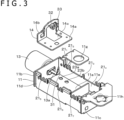
- FIG. 3 is a perspective view of a state where the circuit board and an auxiliary piece are removed.
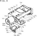
- FIG. 4 is a perspective view of a state where the circuit board and the auxiliary piece are removed, and the tuner module is turned upside down as compared to the one illustrated in FIG. 3 .
- the tuner module includes a tuner case 11, a circuit board 12, an input connector 13, and an auxiliary piece 14. On one surface or both surfaces of the circuit board 12, circuit components that constitute at least part of the tuner module are mounted.
- the tuner case 11 is a metallic case that functions as a shield case. Note that a lid (not illustrated) may cover part of or the entire surface of the circuit board 12. The lid includes a material similar to the material of the tuner case 11.
- the tuner case 11 has a box shape including: a rectangular bottom-surface plate 11a; and a front-surface plate 11b, a back-surface plate 11c, a side-surface plate 11d, and a side-surface plate 11e that are raised from the front, back, left, and right edges of the bottom-surface plate 11a, respectively.
- the tuner case 11 has one open surface.
- hole sections 11g and 11h are screw holes for fixing the tuner module to the housing of a television receiver, for example.
- the circuit board 12 is attached so as to cover the open surface of the tuner case 11.
- An external conductor of the input connector 13 includes a metal such as iron, brass, or zinc.
- a base section of the external conductor of the input connector 13 is attached to the front-surface plate 11b of the tuner case 11 by non-screwing mechanical joining, screwing or the like.
- the input connector 13 is a coaxial connector used for supplying an output of an antenna to a tuner, for example, and is an IEC (International Electrotechnical Commission) connector, for example. It should be noted, however, that the input connector 13 may have another configuration, and may be an F connector, for example.
- One type of F connectors is connected to one end of a coaxial cable, and is called an F connector plug or the like.
- Another type of F connectors is an F connector that receives the center conductor (hereinafter, referred to as the core wire) of a coaxial cable projecting from an F connector plug, and is called an F connector receptacle or the like.
- the core wire of the coaxial cable inserted into the input connector 13 is pinched by two internal spring contact points (pinching pieces).
- the spring contact points constitute at least part of a center electrode, and a terminal section 13a connected with the center electrode is introduced from a rear section of the input connector 13 into the tuner case 11 through a hole formed through the front-surface plate 11b of the tuner case 11 (see FIG. 3 ).
- leg portions 21 projects upward from end surfaces of the side-surface plates of the tuner case 11.
- the leg portions 21 may penetrate holes formed through the circuit board 12.
- the inner walls of the penetrating holes have through-hole structures plated with copper foils on the circuit board 12, are connected with a ground terminal, and make the tuner case 11 serve as a uniform ground potential.
- joints can be formed around the entire circumferences of the through-hole holes of the circuit board 12 in which the leg portions 21 of the tuner case 11 are inscribed, and the mechanical strengths of the joints can be ensured. Note that all the leg portions projecting upward from the tuner case 11 are preferably joined with the holes formed through the circuit board 12.
- the terminal section 13a of the input connector 13 is bent upward at an intermediate portion thereof, and the bent portion serves as a leg portion 31.
- the leg portion 31 may penetrate a hole formed through the circuit board 12.
- the hole has a configuration of a through hole, and serves as a signal terminal on the circuit board 12.
- the auxiliary piece 14 is formed by bending a metal plate of a material similar to the material of the tuner case 11 into an L-shape, and has a base section 14a and a raised section 14b. Center portions of the base section 14a and the raised section 14b are clipped to form an opening 14c.
- the base section 14a of the auxiliary piece 14 is mechanically and electrically connected with the bottom-surface plate 11a of the tuner case 11. Note that both the base section 14a and the raised section 14b may be mechanically and electrically connected with the tuner case 11.
- the opening 14c is formed at a position similar to the position of the hole of the front-surface plate 11b, and the terminal section 13a is introduced into the tuner case 11 through the hole and the opening 14c.
- Methods that can be used for connection between the tuner case 11 and the auxiliary piece 14 include screwing, non-screwing mechanical joining, welding, soldering and the like.
- the terminal section 13a is connected with the core wire of the coaxial cable connected to the input connector 13, and for suppression of radio waves radiated from the terminal section 13a, the length of the terminal section 13a is preferably short.
- the leg portion 31 at the tip of the terminal section 13a may penetrate a through hole formed through the circuit board 12, it becomes difficult to form the through hole at an end section of the circuit board 12 if the length of the terminal section 13a is made short. Accordingly, the length of the terminal section 13a is made short only to the extent that the through hole can be formed at the end section of the circuit board 12.
- Two leg portions 32 and 33 project parallel to each other inward from an upper section of the opening 14c of the raised section 14b of the auxiliary piece 14.
- the leg portions 32 and 33 have approximately similar shapes which are bent upward at intermediate portions thereof.
- the leg portions 32 and 33 are arranged to be positioned near both sides of the leg portion 31 of the terminal section 13a. Accordingly, in a case that the leg portions 31, 32, and 33 are connected to the circuit board 12, the connection locations on the circuit board 12 may be positioned relatively close to each other. Thereby, occurrence of unnecessary radiation can be suppressed.
- the leg portions 32 and 33 are connected with the tuner case 11, the leg portions 32 and 33 serve as ground terminals.
- the auxiliary piece 14 may not be used, but by sheet metal working, for example, an external conductor of the input connector 13 may be cut, and the cut portions may be raised. The method leads to more significant deterioration of the strength of the input connector 13, and there is a fear that when a load is applied to the input connector 13 by a coaxial cable connected to the input connector 13 at the time of actual use, the input connector 13 may be damaged.
- the leg portions are undesirably located closer to the input connector 13, it becomes necessary to form holes, through which the leg portions are to be inserted, near an end section of the circuit board 12, and there is a fear that the circuit board 12 may be damaged. Furthermore, the method of forming the leg portions by processing of cutting the tuner case 11 itself and raising the cut portions necessitates forming holes through the tuner case 11, and gives rise to a problem that radiation from the holes is caused.
- the auxiliary piece 14 is used.
- the auxiliary piece 14 assists connection between the tuner case 11 and the circuit board 12 that serve as a ground potential.
- the base section 14a of the auxiliary piece 14 is in surface-contact with the bottom-surface plate 11a of the tuner case 11, thereby realizing a low contact resistance.
- a plurality of protrusions 22a, 22b, 22c, and 22d projecting from the base section 14a is formed, and holes 23a, 23b, 23c, and 23d are formed at positions on the bottom-surface plate 11a that correspond to the protrusions 22a to 22d.
- the protrusions 22a to 22d fit to the holes 23a to 23d, thereby making it possible to surely realize the surface-contact.
- all the ground connecting sections between the tuner case 11 and the circuit board 12 can be soldered connections around the entire circumferences of the through-hole hole sections. Accordingly, solder joints in which a direct current and a high-frequency resistance between grounds of the input connector, the nearby tuner case, and the circuit board can be made very small can be realized, and strong connections can be established.
- the intervals between the inner walls of the through holes and the inserted leg portions of the tuner case 11 are very narrow, and solder melted in a reflow oven experiences capillary action, and is drawn into the intervals, thereby making it possible to realize strong joints simply and conveniently.
- a semifinished product of a tuner on which surface mount components are mounted on a circuit board is created.
- the surface mount components are mounted in such a manner that the surface mount components come into contact with the solder printed by a robot machine having nozzles that suctionally attract the surface mount components, and the solder is melted by first heating by the reflow oven and joined with the surface mount components.
- a tuner case of the tuner is inserted into a slit section provided to the circuit board, and is joined by second heating by the reflow oven.
- the solder printing described above is a typical construction method (screen printing) of performing printing by using an aluminum screen of approximately 0.1 mm, and can fix many electronic components onto the circuit board while ensuring conduction therebetween.
- FIG. 5 is for explaining the second reflow process.
- a circuit board 101 is inverted before insertion of a tuner case, and on a side opposite to surface mount components 102, solder 105 pushed into nozzles 104 by a laterally-sliding squeegee 103 is applied onto the board 101 in accordance with the principle of what is called mimeograph printing (collective application of solder).
- mimeograph printing collective application of solder
- the circuit board 101 is inverted again (board inversion).
- the reference signs 106a and 106b indicate copper foils.
- a mechanical component 107 such as a tuner case is mounted, and as illustrated in FIG. 5D , the mechanical component 107 is joined by second reflowing.
- the nozzles 104 need to be designed and manufactured as dedicated facilities optimized for individual tuners, and care is also required regarding the viscosity and granularity of the solder 105, before being cured, to be applied by being caused to pass through the nozzles 104.
- care is also required regarding heat stress on the surface mount components 102.
- the method of applying solder to fill the through-hole holes can be performed by printing on a surface where the surface mount components 102 are mounted by application of a screen. Accordingly, it is possible to make the nozzles 104 unnecessary, and the problems mentioned above can be solved.
- the portion near the input connector 13 serves as a portion where conversion is performed such that what is called high-frequency signals, such as UHF-band signals or IF signals for satellite broadcasting, flowing through a coaxial line is made to flow through a planar circuit on the circuit board 12.
- high-frequency signals such as UHF-band signals or IF signals for satellite broadcasting
- the leg portions 32 and 33 are provided.
- high-frequency signals are supplied to a signal processing section (referred to as a planar circuit) on the circuit board 12 through the coaxial cable and the input connector 13. That is, signals are transmitted from the coaxial cable to the planar circuit. The point is examined.
- a signal processing section referred to as a planar circuit
- a coaxial cable has a center conductor (core wire) 51 and an external conductor 53 that covers the center conductor 51 with a dielectric 52 being interposed therebetween.
- the circumference of the external conductor 53 is covered by a protection cover (not illustrated).
- a current flows inside the center conductor 51 and the external conductor 53.
- a current from a signal source located at one end of the coaxial cable flows through the center conductor 51 to a load on the other end side, and furthermore passes through the external conductor 53 to return to the signal source on the one end side.
- FIG. 7A and FIG. 7B illustrate the configuration of a microstrip line in which a conductor line 55 is provided on one surface of a dielectric board 54, and a ground conductor surface 56 is provided on the other surface of the dielectric board 54.
- High-frequency signals are transmitted from a coaxial cable to a surface circuit represented by a microstrip line, and are converted into the shape of flux line and lines of electric force as illustrated in FIG. 7B .
- the portion near the connector connecting section is designed in according with the basic theory mentioned above, and it is found that a connection with a ground potential established by the auxiliary piece 14 is the most effective connection.
- FIG. 8 is a perspective view illustrating a configuration example of the tuner module according to the second embodiment of the present technology.
- FIG. 9 is a perspective view of a state where a circuit board is removed.
- FIG. 10 is a perspective view of a state where the circuit board and an auxiliary piece are removed.
- the second embodiment adopts a biaxial configuration obtained by adding an input connector 113 to the configuration of the first embodiment.
- digital terrestrial broadcasting reception signals are supplied to the input connector 13, and satellite broadcasting IF signals are supplied to the input connector 113.
- the tuner module includes a tuner case 111, a circuit board 112, the input connectors 13 and 113, and an auxiliary piece 114. On one surface or both surfaces of the circuit board 112, circuit components that constitute at least part of the tuner module are mounted.
- the tuner case 111 is a metallic case that functions as a shield case.
- a lid (not illustrated) may cover part of or the entire surface of the circuit board 112.
- the lid includes a material similar to the material of the tuner case 111.
- the tuner case 111 has a box shape including: a rectangular bottom-surface plate 111a; and a front-surface plate 111b, a back-surface plate 111c, a side-surface plate 111d, and a side-surface plate 111e that are raised from the front, back, left, and right edges of the bottom-surface plate 111a, respectively.
- the tuner case 111 has one open surface.
- hole sections 111g and 111h are screw holes for fixing the tuner module to the housing of a television receiver, for example.
- the circuit board 112 is attached so as to cover the open surface of the tuner case 111.
- External conductors of the input connectors 13 and 113 include a metal such as iron, brass, or zinc. Base sections of the external conductors of the input connectors 13 and 113 are attached to the front-surface plate 111b of the tuner case 111 by non-screwing mechanical joining, screwing or the like.
- the input connectors 13 and 113 are coaxial connectors used for supplying outputs of antennas to a tuner, for example.
- the input connector 113 is an F connector, for example. It should be noted, however, that, similarly to the input connector 13, the input connector 113 may be an IEC connector.
- the core wires of coaxial cables inserted into the input connectors 13 and 113 are each pinched by two internal spring contact points (pinching pieces).
- the spring contact points constitute at least part of center electrodes, and terminal sections 13a and 113a connected with the center electrodes are introduced from rear sections of the input connectors 13 and 113 into the tuner case 111 through holes formed on the front-surface plate 111b of the tuner case 111 (see FIG. 10 ).
- a plurality of leg portions projects upward from end surfaces of the side-surface plates 111d and 111e and the back-surface plate 111c of the tuner case 111. Furthermore, a plurality of plate-like bodies is provided on the bottom-surface plate 111a of the tuner case 111, and leg portions are provided on the upper end surfaces of the plurality of plate-like bodies. The leg portions are inserted into through holes provided as ground terminals of the circuit board 112, and soldered. Some of the plurality of plate-like bodies are provided to surround areas of corner sections of the tuner case 111 where the respective input connectors 13 and 113 are provided.
- the plate-like bodies include a metal similar to the metal of the tuner case 111, and function as shield members. Note that the auxiliary piece 114 may integrally have plate-like bodies that have similar functions.
- the leg portions may penetrate holes formed through the circuit board 112.
- the inner walls of the penetrating holes have through-hole structures plated with copper foils on the circuit board 112, are connected with a ground terminal, and make the tuner case 111 serve as a uniform ground potential.
- joints can be formed around the entire circumferences of the through-hole holes of the circuit board 112 in which the leg portions of the tuner case 111 are inscribed, and the mechanical strengths of the joints can be ensured. Note that all the leg portions projecting upward from the tuner case 111 are preferably joined with the holes formed through the circuit board 112.
- the terminal section 13a of the input connector 13 and the terminal section 113a of the input connector 113 are bent upward at intermediate portions thereof, and the bent portions serve as leg portions 31 and 131, respectively.
- the leg portions 31 and 131 may penetrate holes formed through the circuit board 112.
- the holes have configurations of through holes, and serve as signal terminals on the circuit board 112.
- the auxiliary piece 114 is formed by bending a metal plate of a material similar to the material of the tuner case 111 into an L-shape, and has a base section 114a and a raised section 114b. Center portions of the base section 114a and the raised section 114b are clipped to form an opening 114c.
- the base section 114a of the auxiliary piece 114 is mechanically and electrically connected with the bottom-surface plate 111a of the tuner case 11. Note that both the base section 114a and the raised section 114b may be mechanically and electrically connected with the tuner case 111.
- the opening 114c is formed at a position similar to the position of the hole of the front-surface plate 111b, and the terminal section 13a is introduced into the tuner case 111 through the hole and the opening 114c.
- Methods that can be used for connection between the tuner case 111 and the auxiliary piece 114 include screwing, non-screwing mechanical joining, welding, soldering and the like.
- the terminal section 13a is connected with the core wire of the coaxial cable connected to the connector 13, and for suppression of radio waves radiated from the terminal section 13a, the length of the terminal section 13a is preferably short.
- the leg portion 31 at the tip of the terminal section 13a may penetrate a through hole formed through the circuit board 112, it becomes difficult to form the through hole at an end section of the circuit board 112 if the length of the terminal section 13a is made short. Accordingly, the length of the terminal section 13a is made short only to the extent that the through hole can be formed at the end section of the circuit board 112.
- Two leg portions 32 and 33 project parallel to each other inward from an upper section of the opening 114c of the raised section 114b of the auxiliary piece 114.
- the leg portions 32 and 33 have approximately similar shapes which are bent upward at intermediate portions thereof.
- the leg portions 32 and 33 are arranged to be positioned near both sides of the leg portion 31 of the terminal section 13a. Accordingly, in a case that the leg portions 31, 32, and 33 are connected to the circuit board 112, the connection locations on the circuit board 112 may be positioned relatively close to each other. Thereby, occurrence of unnecessary radiation can be suppressed.
- the leg portions 32 and 33 are connected with the tuner case 111, the leg portions 32 and 33 serve as ground terminals.
- the auxiliary piece 114 may not be used, but by sheet metal working, for example, an external conductor of the input connector 13 may be cut, and the cut portions may be raised. The method leads to more significant deterioration of the strength of the input connector 13, and there is a fear that when a load is applied to the input connector 13 by a coaxial cable connected to the input connector 13 at the time of actual use, the input connector 13 may be damaged.
- leg portions connected with the core wire of the input connector 13 are undesirably located closer to the input connector 13, and there is a fear that when holes through which the leg portions are to be inserted are formed near an end section of the circuit board 112, the circuit board 112 may be damaged.
- the method of forming the leg portions by processing of cutting the tuner case 111 itself and raising the cut portions necessitates forming holes through the tuner case 111, and gives rise to a problem that radiation from the holes is caused.
- the auxiliary piece 114 is used.
- the auxiliary piece 114 assists connection between the tuner case 111 and the circuit board 112 that serve as a ground potential.
- the base section 114a of the auxiliary piece 114 is in surface-contact with the bottom-surface plate 111a of the tuner case 111, thereby realizing a low contact resistance.
- solder joints in which a direct current and a high-frequency resistance between grounds of the input connector, the nearby tuner case, and the circuit board can be made very small can also be realized, and strong connections can be established.
- a leg portion 132 for connection with the ground terminals is provided near the terminal section 113a of the input connector 113.
- FIG. 11 is a perspective view illustrating a configuration example of the tuner module according to the third embodiment of the present technology.
- FIG. 12 is a perspective view of a state where a circuit board is removed.
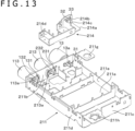
- FIG. 13 is a perspective view of a state where the circuit board and an auxiliary piece are removed.
- the third embodiment adopts a triaxial configuration obtained by adding an input connector 213 between the input connector 13 and the input connector 113 in the configuration in the second embodiment.
- digital terrestrial broadcasting reception signals are supplied to the input connector 13, and satellite broadcasting IF signals are supplied to the input connectors 113 and 213.
- the tuner module includes a tuner case 211, a circuit board 212, the input connectors 13, 113, and 213, and an auxiliary piece 214. On one surface or both surfaces of the circuit board 212, circuit components that constitute at least part of the tuner module are mounted.
- the tuner case 211 is a metallic case that functions as a shield case.
- a lid (not illustrated) may cover part of or the entire surface of the circuit board 212.
- the lid includes a material similar to the material of the tuner case 211.
- the tuner case 211 has a box shape including: a rectangular bottom-surface plate 211a; and a front-surface plate 211b, a back-surface plate 211c, a side-surface plate 211d, and a side-surface plate 211e that are raised from the front, back, left, and right edges of the bottom-surface plate 211a, respectively.
- the tuner case 211 has one open surface.
- hole sections 211g and 211h are screw holes for fixing the tuner module to the housing of a television receiver, for example.
- the circuit board 212 is attached so as to cover the open surface of the tuner case 211.
- External conductors of the input connectors 13, 113, and 213 include a metal such as iron, brass, or zinc. Base sections of the external conductors of the input connectors 13, 113, and 213 are attached to the front-surface plate 211b of the tuner case 211 by non-screwing mechanical joining, screwing or the like.
- the input connectors 13, 113, and 213 are coaxial connectors used for supplying outputs of antennas to a tuner, for example.
- the input connectors 113 and 213 are F connectors, for example. It should be noted, however, that, similarly to the input connector 13, the input connectors 113 and 213 may be IEC connectors.
- the core wires of coaxial cables inserted into the input connectors 13, 113, and 213 are each pinched by two internal spring contact points (pinching pieces).
- the spring contact points constitute at least part of center electrodes, and terminal sections 13a, 113a, and 213a connected with the center electrodes are introduced from rear sections of the input connectors 13, 113, and 213 into the tuner case 211 through holes formed on the front-surface plate 211b of the tuner case 211 (see FIG. 12 ).
- a plurality of leg portions projects upward from end surfaces of the side-surface plates 211d and 211e and the back-surface plate 211c of the tuner case 211. Furthermore, a plurality of plate-like bodies is provided on the bottom-surface plate 211a of the tuner case 211, and a plate-like body 214d is provided on the auxiliary piece 214 mentioned below. Leg portions are provided on the upper end surfaces of the plate-like bodies. The leg portions are inserted into through holes provided as ground terminals of the circuit board 112, and soldered. Some of the plurality of plate-like bodies are provided to surround areas of the tuner case 211 where the respective input connectors 13, 113, and 213 are provided.
- the plate-like bodies include a metal similar to the metal of the tuner case 211, and function as shield members.
- the leg portions may penetrate holes formed through the circuit board 212.
- the inner walls of the penetrating holes have through-hole structures plated with copper foils on the circuit board 212, are connected with a ground terminal, and make the tuner case 211 serve as a uniform ground potential.
- joints can be formed around the entire circumferences of the through-hole holes of the circuit board 212 in which the leg portions of the tuner case 211 are inscribed, and the mechanical strengths of the joints can be ensured. Note that all the leg portions projecting upward from the tuner case 211 are preferably joined with the holes formed through the circuit board 212.
- the terminal section 13a of the input connector 13, the terminal section 113a of the input connector 113, and the terminal section 213a of the input connector 213 are bent upward at intermediate portions thereof, and the bent portions serve as leg portions 31, 131, and 231, respectively.
- the leg portions 31, 131, and 231 may penetrate holes formed through the circuit board 212.
- the holes have configurations of through holes, and serve as signal terminals on the circuit board 212.
- the auxiliary piece 214 is formed by bending a metal plate of a material similar to the material of the tuner case 211 into an L-shape, and has a base section 214a and a raised section 214b. Center portions of the base section 214a and the raised section 214b are clipped to form an opening 214c.
- the auxiliary piece 214 has the plate-like body 214d as a shield member between the input connectors 113 and 213.
- the base section 214a of the auxiliary piece 214 is mechanically and electrically connected with the bottom-surface plate 211a of the tuner case 211. Note that both the base section 214a and the raised section 214b may be mechanically and electrically connected with the tuner case 211.
- the opening 214c is formed at a position similar to the position of the hole of the front-surface plate 211b, and the terminal section 13a is introduced into the tuner case 211 through the hole and the opening 214c.
- Methods that can be used for connection between the tuner case 211 and the auxiliary piece 214 include screwing, non-screwing mechanical joining, welding, soldering and the like.
- the terminal section 213a is connected with the core wire of the coaxial cable connected to the input connector 213, and for suppression of radio waves radiated from the terminal section 213a, the length of the terminal section 213a is preferably short.
- the leg portion 231 at the tip of the terminal section 213a may penetrate a through hole formed through the circuit board 212, it becomes difficult to form the through hole at an end section of the circuit board 212 if the length of the terminal section 213a is made short. Accordingly, the length of the terminal section 213a is made short only to the extent that the through hole can be formed at the end section of the circuit board 212.
- Two leg portions 32 and 33 project parallel to each other inward from an upper section of the opening 214c of the raised section 214b of the auxiliary piece 214.
- the leg portions 32 and 33 have approximately similar shapes which are bent upward at intermediate portions thereof.
- the leg portions 32 and 33 are arranged to be positioned near both sides of the leg portion 31 of the terminal section 213a. Accordingly, in a case that the leg portions 31, 32, and 33 are connected to the circuit board 212, the connection locations on the circuit board 212 may be positioned relatively close to each other. Thereby, occurrence of unnecessary radiation can be suppressed.
- the leg portions 32 and 33 are connected with the tuner case 211, the leg portions 32 and 33 serve as ground terminals.
- the auxiliary piece 214 may not be used, but by sheet metal working, for example, an external conductor of the input connector 13 may be cut, and the cut portions may be raised. The method leads to more significant deterioration of the strength of the input connector 13, and there is a fear that when a load is applied to the input connector 13 by a coaxial cable connected to the input connector 13 at the time of actual use, the input connector 13 may be damaged.
- leg portions connected with the core wire of the input connector 13 are undesirably located closer to the input connector 13, and there is a fear that when holes through which the leg portions are to be inserted are formed near an end section of the circuit board 212, the circuit board 212 may be damaged.
- the method of forming the leg portions by processing of cutting the tuner case 211 itself and raising the cut portions necessitates forming holes through the tuner case 211, and gives rise to a problem that radiation from the holes is caused.
- the auxiliary piece 214 is used.
- the auxiliary piece 214 assists connection between the tuner case 211 and the circuit board 212 that serve as a ground potential.
- the base section 214a of the auxiliary piece 214 is in surface-contact with the bottom-surface plate 211a of the tuner case 211, thereby realizing a low contact resistance.
- leg portions 132 and 232 for connection with the ground terminals are provided near the terminal sections 113a and 213a of the input connectors 113 and 213, respectively.
- all the ground connecting sections between the tuner case 211 and the circuit board 212 can be soldered connections around the entire circumferences of the through-hole hole sections. Accordingly, solder joints in which a direct current and a high-frequency resistance between grounds of the input connector, the nearby tuner case, and the circuit board can be made very small can be realized.
- the present technology is suitable for tuner modules of advanced BS receiving devices (to be put on the market as 4K and 8K television television) that receive the frequency range that covers 3.2 GHz as a result of the future expansion of the reception band.
- the intervals between the inner walls of the through holes and the inserted leg portions of the tuner case 211 are very narrow, and solder melted in a reflow oven experiences capillary action and is drawn into the intervals, thereby making it possible to realize strong joints simply and conveniently.
- the auxiliary piece is arranged to block the opening sections of the tuner case.
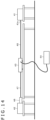
- FIG. 14 illustrates one example of a device for measuring the effects of the present technology. That is, the configuration illustrates a system for measurement of coaxial-line shielding effects called S4 indicated in the standard called EN55020 stipulated by the European Committee for Electrotechnical Standardization called Cenelec in Europe.
- a measurement-target tuner 41, a desired signal generator 42, a measuring probe 43, and an EMI (Electro-Magnetic Interference: electro-magnetic interference) measurement device 44 are provided.
- An antenna-signal input connector 41a of the measurement-target tuner 41 and the measuring probe 43 are connected by a coaxial cable (75 ⁇ ) 45, and the desired signal generator 42 and the measuring probe 43 are connected by an impedance matching device 46 and a coaxial cable 47.
- the impedance matching device 46 performs impedance conversion (50 Q ⁇ 75 ⁇ ).
- a high-frequency signal generated by the desired signal generator 42 is supplied to the measurement-target tuner 41, and a leaked signal induced to the outer covering (ground line) of the coaxial cable 45 by the measuring probe 43 is measured by the EMI measurement device 44. Measurement is performed for determining that the shielding effect of the coaxial cable 45 does not deteriorate due to an input circuit of the measurement-target tuner 41.
- Table 1 illustrates one example of measurement results. Table 1 illustrates measurement values obtained by using 950 MHz with which the lowest shielding effect has been obtained.
- the sample without an auxiliary piece corresponds to a measurement result of a conventional tuner module, and the sample A and the sample B to which auxiliary pieces are added correspond to tuner modules to which the present technology is applied.
- the present technology can improve shielding amounts.
- an IC circuit as a terrestrial television broadcasting (TV) tuner-module function section or an IC (circuit) as a satellite broadcasting (BS) tuner-module function section, and electronic components are formed (mounted) on the circuit boards of the tuner modules described as the first embodiment, the second embodiment, and the third embodiment mentioned above.
- the tuner-module boards are mounted on circuit boards of television receivers, as one example.
- a receiving device is at least partially constituted by using any of the tuner modules.
- the receiving device is configured to be able to receive terrestrial television broadcasting wave signals and satellite broadcasting wave signals, for example.
- the receiving device has a reception antenna that receives broadcasting wave signals, a tuner module having a frequency conversion function, and a demodulating section.
- a first system of the receiving device includes a reception antenna, an antenna connector, a filter, a low-noise amplifier (Low Noise Amplifier: LNA), a tuner section, and a demodulating section.
- a second system of the receiving device includes a reception antenna, an antenna connector, a filter, a low-noise amplifier (LNA), a tuner section, and a demodulating section.
- LNA Low Noise Amplifier
- the input connector 13 is an IEC connector
- the input connector 13 may be an F connector.
- FIG. 15, FIG. 16 , FIG. 17 , and FIG. 18 illustrate the configuration in a case that an F connector 113 is used. Detailed explanations of the configuration are omitted since the configuration is similar to the configuration illustrated in FIG. 1, FIG. 2 , FIG. 3 , and FIG. 4 , and the configuration has the leg portion 131 and the leg portions 132 and 133 of the auxiliary piece 114.
Landscapes
- Engineering & Computer Science (AREA)
- Microelectronics & Electronic Packaging (AREA)
- Signal Processing (AREA)
- Multimedia (AREA)
- Computer Networks & Wireless Communication (AREA)
- Structure Of Receivers (AREA)
Claims (8)
- Tunermodul, umfassend:einen Eingangsverbinder (13), der einen Anschlussabschnitt (13a) umfasst, der mit einer Mittelelektrode des Eingangsverbinders verbunden ist, wobei der Anschlussabschnitt einen Beinabschnitt (31) aufweist;ein Tunergehäuse (11);eine Leiterplatte (12); undein Hilfsstück (14), wobeidas Hilfsstück eine Oberfläche des Tunergehäuses berührt und an der Oberfläche des Tunergehäuses befestigt ist, wobeiein erster und ein zweiter Beinabschnitt (32, 33) des Hilfsstücks als Erdungspotential mit der Leiterplatte verbunden sind, und der erste und der zweite Beinabschnitt des Hilfsstücks so angeordnet sind, dass sie in der Nähe beider Seiten des Beinabschnitts des Anschlussabschnitts positioniert sind, um Funkwellen zu unterdrücken, die von einer Verbindungsstelle auf der Leiterplatte für den Beinabschnitt des Anschlussabschnitts abgestrahlt werden.
- Tunermodul nach Anspruch 1, wobei eine Vielzahl von Eingangsanschlüssen an einer Oberfläche des Tunergehäuses befestigt ist.
- Tunermodul nach Anspruch 1, wobei die Oberfläche des Tunergehäuses, an der das Zusatzteil befestigt ist, eine Oberfläche einschließt, an der der Eingangsanschluss befestigt ist.
- Tunermodul nach Anspruch 1, wobei ein Loch, mit dem das Hilfsstück als Erdungspotential der Leiterplatte verbunden ist, durch Durchkontaktierung gebildet wird.
- Tunermodul nach Anspruch 1, wobei eine Passung zwischen einem Loch und einem Vorsprung, die zur Fixierung dienen, für einen Verbindungsabschnitt des Hilfsstücks und des Tunergehäuses verwendet wird.
- Tunermodul nach Anspruch 1, wobei das Hilfsstück durch eine Lötverbindung mit der Oberfläche des Tunergehäuses gekoppelt ist.
- Tunermodul nach Anspruch 1, wobei das Hilfsstück durch eine mechanische Verbindung ohne Schrauben mit der Oberfläche des Tunergehäuses gekoppelt ist.
- Empfangsvorrichtung, umfassend das Tunermodul nach Anspruch 1.
Applications Claiming Priority (2)
| Application Number | Priority Date | Filing Date | Title |
|---|---|---|---|
| JP2017227782 | 2017-11-28 | ||
| PCT/JP2018/037337 WO2019106957A1 (ja) | 2017-11-28 | 2018-10-05 | チューナモジュール及び受信装置 |
Publications (3)
| Publication Number | Publication Date |
|---|---|
| EP3720005A1 EP3720005A1 (de) | 2020-10-07 |
| EP3720005A4 EP3720005A4 (de) | 2021-04-28 |
| EP3720005B1 true EP3720005B1 (de) | 2025-02-26 |
Family
ID=66664786
Family Applications (1)
| Application Number | Title | Priority Date | Filing Date |
|---|---|---|---|
| EP18883263.8A Active EP3720005B1 (de) | 2017-11-28 | 2018-10-05 | Tunermodul und empfangsvorrichtung |
Country Status (5)
| Country | Link |
|---|---|
| US (1) | US11395418B2 (de) |
| EP (1) | EP3720005B1 (de) |
| JP (1) | JP7251736B2 (de) |
| CN (1) | CN111373664B (de) |
| WO (1) | WO2019106957A1 (de) |
Families Citing this family (2)
| Publication number | Priority date | Publication date | Assignee | Title |
|---|---|---|---|---|
| USD867994S1 (en) * | 2016-12-22 | 2019-11-26 | Sony Semiconductor Solutions Corporation | Tuner |
| KR102901575B1 (ko) * | 2023-12-26 | 2025-12-22 | 엘지전자 주식회사 | 글로벌 통합 튜너 장치 및 그의 제어 방법 |
Family Cites Families (43)
| Publication number | Priority date | Publication date | Assignee | Title |
|---|---|---|---|---|
| JPH05259926A (ja) * | 1992-03-09 | 1993-10-08 | Funai Electric Co Ltd | コネクタ入力チューナー |
| JP3271128B2 (ja) * | 1993-09-20 | 2002-04-02 | ソニー株式会社 | チューナケース |
| JP3444727B2 (ja) * | 1995-09-26 | 2003-09-08 | シャープ株式会社 | デジタル方式衛星放送受信機 |
| JP3537299B2 (ja) * | 1997-10-13 | 2004-06-14 | アルプス電気株式会社 | テレビジョンチュ−ナ |
| JP2002135140A (ja) * | 2000-10-24 | 2002-05-10 | Sharp Corp | 送受信機用フロントエンド |
| JP3601497B2 (ja) * | 2001-10-03 | 2004-12-15 | 松下電器産業株式会社 | 高周波装置 |
| EP1553761B1 (de) * | 2002-07-25 | 2009-08-26 | Sony Corporation | Empfängereinrichtung und fernsehempfänger |
| CN100405744C (zh) * | 2003-02-25 | 2008-07-23 | 索尼计算机娱乐公司 | 调谐单元、接收装置和电子机器 |
| US6944011B2 (en) * | 2003-06-13 | 2005-09-13 | Gary T. Krajecki | Electronic device cable cover |
| EP1509041A1 (de) * | 2003-08-19 | 2005-02-23 | Medion AG | Multifunktionsgerät zur Audio/Videosignal-Verarbeitung |
| JP2005102151A (ja) * | 2003-08-27 | 2005-04-14 | Sony Corp | デジタル放送受信用チューナ |
| KR100998395B1 (ko) * | 2003-09-19 | 2010-12-03 | 파나소닉 주식회사 | 디지털 텔레비전 수신기용 모듈 및 그것을 구비한 디지털텔레비전 수신기 |
| US20050227744A1 (en) * | 2004-04-08 | 2005-10-13 | Yen-Fu Chiang | System and method for a simplified cable tuner |
| CN2738473Y (zh) | 2004-04-29 | 2005-11-02 | 皇家飞利浦电子股份有限公司 | 具有标准连接器的扁平调谐器模块 |
| JP4621466B2 (ja) * | 2004-09-30 | 2011-01-26 | 株式会社東芝 | チューナ装置 |
| JP2006157087A (ja) * | 2004-11-25 | 2006-06-15 | Orion Denki Kk | 不要輻射防止手段を備えたチューナー回路基板及び電子機器 |
| JP4063841B2 (ja) * | 2005-09-09 | 2008-03-19 | シャープ株式会社 | 受信装置、受信システム |
| JP4350084B2 (ja) * | 2005-11-07 | 2009-10-21 | シャープ株式会社 | 受信装置、受信システム |
| JP2007251702A (ja) * | 2006-03-17 | 2007-09-27 | Sharp Corp | 受信装置、受信システム |
| JP4659666B2 (ja) * | 2006-04-18 | 2011-03-30 | 株式会社日立製作所 | 放送受信装置、及び、そのチューナ装置とそのための分配器 |
| KR100818477B1 (ko) * | 2006-06-14 | 2008-04-02 | 삼성전기주식회사 | 싱글 패키지 텔레비전 튜닝 장치 및 텔레비전 수신기 |
| US7733659B2 (en) * | 2006-08-18 | 2010-06-08 | Delphi Technologies, Inc. | Lightweight audio system for automotive applications and method |
| JP2009290085A (ja) * | 2008-05-30 | 2009-12-10 | Alps Electric Co Ltd | 高周波ユニット |
| JP2010021494A (ja) | 2008-07-14 | 2010-01-28 | Sony Corp | チューナ装置 |
| JP4938073B2 (ja) * | 2009-11-10 | 2012-05-23 | シャープ株式会社 | 放送受信装置 |
| JP2011139321A (ja) * | 2009-12-28 | 2011-07-14 | Sony Corp | チューナモジュールおよび受信装置 |
| JP2012039595A (ja) * | 2010-07-12 | 2012-02-23 | Sony Corp | フロントエンドモジュールおよび受信装置 |
| JP5630118B2 (ja) | 2010-07-22 | 2014-11-26 | ソニー株式会社 | チューナモジュールおよび受信装置 |
| KR101320191B1 (ko) * | 2010-12-30 | 2013-10-23 | 삼성전기주식회사 | 복합 튜너 모듈 |
| CN103858067A (zh) * | 2011-03-09 | 2014-06-11 | 汤姆逊许可公司 | 具有卡扣式热沉和智能卡读取器的机顶盒或服务器 |
| JP5686066B2 (ja) | 2011-08-04 | 2015-03-18 | ソニー株式会社 | チューナモジュール及び受信装置 |
| KR20130035675A (ko) * | 2011-09-30 | 2013-04-09 | 삼성전기주식회사 | 튜너 모듈 |
| WO2013136639A1 (ja) * | 2012-03-13 | 2013-09-19 | パナソニック株式会社 | 薄型表示装置 |
| JP5349641B2 (ja) * | 2012-04-25 | 2013-11-20 | 株式会社東芝 | 電子機器 |
| EP2873312A4 (de) * | 2012-07-16 | 2016-03-16 | Thomson Licensing | Armatur zum entfernen von abdeckungen |
| JP2014216933A (ja) * | 2013-04-26 | 2014-11-17 | 株式会社東芝 | テレビジョン受像機および電子機器 |
| CN203522900U (zh) * | 2013-09-27 | 2014-04-02 | 深圳华立视通科技有限公司 | 调谐器 |
| PL2863496T3 (pl) * | 2013-10-18 | 2018-02-28 | Wöhner GmbH & Co. KG Elektrotechnische Systeme | System ochrony przed dotykiem do prądowych szyn zbiorczych |
| KR102088912B1 (ko) * | 2013-11-13 | 2020-03-13 | 엘지전자 주식회사 | 영상표시장치 |
| US9839145B2 (en) * | 2014-01-24 | 2017-12-05 | Lg Electronics Inc. | Display device |
| JP6338976B2 (ja) * | 2014-08-29 | 2018-06-06 | 株式会社東芝 | 電子機器、取付部材、および取付方法 |
| WO2018163588A1 (ja) * | 2017-03-06 | 2018-09-13 | ソニーセミコンダクタソリューションズ株式会社 | チューナモジュール及び受信装置 |
| US11189909B2 (en) * | 2018-08-30 | 2021-11-30 | Apple Inc. | Housing and antenna architecture for mobile device |
-
2018
- 2018-10-05 CN CN201880075526.2A patent/CN111373664B/zh active Active
- 2018-10-05 JP JP2019557042A patent/JP7251736B2/ja active Active
- 2018-10-05 WO PCT/JP2018/037337 patent/WO2019106957A1/ja not_active Ceased
- 2018-10-05 US US16/766,060 patent/US11395418B2/en active Active
- 2018-10-05 EP EP18883263.8A patent/EP3720005B1/de active Active
Also Published As
| Publication number | Publication date |
|---|---|
| CN111373664B (zh) | 2022-07-29 |
| JP7251736B2 (ja) | 2023-04-04 |
| JPWO2019106957A1 (ja) | 2020-12-03 |
| US20200352040A1 (en) | 2020-11-05 |
| CN111373664A (zh) | 2020-07-03 |
| EP3720005A1 (de) | 2020-10-07 |
| EP3720005A4 (de) | 2021-04-28 |
| WO2019106957A1 (ja) | 2019-06-06 |
| US11395418B2 (en) | 2022-07-19 |
Similar Documents
| Publication | Publication Date | Title |
|---|---|---|
| TWI760178B (zh) | 連接器組裝體 | |
| US9661791B2 (en) | RF interference suppressor | |
| US11404809B2 (en) | Electrical connector assembly with shielding shells surrounding each of first and second connectors | |
| US9775268B2 (en) | Receiving device and shield case connection method | |
| EP3720005B1 (de) | Tunermodul und empfangsvorrichtung | |
| CN110692169A (zh) | 便携式电子设备 | |
| CN106960997A (zh) | 封闭金属腔毫米波微带传输线 | |
| US6818837B2 (en) | Wiring connection structure and transmitter using the same | |
| CN208488503U (zh) | 测试设备 | |
| CN205488838U (zh) | 插式连接器 | |
| CN108155499A (zh) | 板对板型射频插头、插座及其连接器组件 | |
| WO2022256099A1 (en) | Connector and method for connecting a coaxial cable to a printed circuit board | |
| EP3297092B1 (de) | Kabel und hochfrequenzvorrichtung damit | |
| JP2017069138A (ja) | コネクタ、送受信モジュールおよび送受信モジュールの製造方法 | |
| TWI651028B (zh) | 用於射頻測試之銲墊結構 | |
| JP2021093365A (ja) | シールドされた基板対基板コネクタ | |
| US11291145B2 (en) | Integrated antenna device | |
| JP3645494B2 (ja) | 相互変調歪測定システム | |
| CN108155498A (zh) | 板对板型射频插头及其连接器组件 | |
| RU2322738C1 (ru) | Усилительный блок антенного тракта приемника сигналов спутниковых систем | |
| RU137801U1 (ru) | Конструкция герметичного соединения корпуса и коаксиально-полоскового соединителя | |
| JPH10126190A (ja) | Emi用フィルタ回路 | |
| JP2005249744A (ja) | 透過特性測定装置及び方法 | |
| Santamaria et al. | A comparison of unshielded wire to shielded wire with shields terminated using pigtail and shields terminated through a conducting elastomer | |
| WO2006073336A1 (en) | Emc connector assembly |
Legal Events
| Date | Code | Title | Description |
|---|---|---|---|
| STAA | Information on the status of an ep patent application or granted ep patent |
Free format text: STATUS: THE INTERNATIONAL PUBLICATION HAS BEEN MADE |
|
| PUAI | Public reference made under article 153(3) epc to a published international application that has entered the european phase |
Free format text: ORIGINAL CODE: 0009012 |
|
| STAA | Information on the status of an ep patent application or granted ep patent |
Free format text: STATUS: REQUEST FOR EXAMINATION WAS MADE |
|
| 17P | Request for examination filed |
Effective date: 20200514 |
|
| AK | Designated contracting states |
Kind code of ref document: A1 Designated state(s): AL AT BE BG CH CY CZ DE DK EE ES FI FR GB GR HR HU IE IS IT LI LT LU LV MC MK MT NL NO PL PT RO RS SE SI SK SM TR |
|
| AX | Request for extension of the european patent |
Extension state: BA ME |
|
| DAV | Request for validation of the european patent (deleted) | ||
| DAX | Request for extension of the european patent (deleted) | ||
| A4 | Supplementary search report drawn up and despatched |
Effective date: 20210330 |
|
| RIC1 | Information provided on ipc code assigned before grant |
Ipc: H04B 1/08 20060101AFI20210324BHEP Ipc: H05K 7/14 20060101ALI20210324BHEP |
|
| STAA | Information on the status of an ep patent application or granted ep patent |
Free format text: STATUS: EXAMINATION IS IN PROGRESS |
|
| 17Q | First examination report despatched |
Effective date: 20220314 |
|
| GRAP | Despatch of communication of intention to grant a patent |
Free format text: ORIGINAL CODE: EPIDOSNIGR1 |
|
| STAA | Information on the status of an ep patent application or granted ep patent |
Free format text: STATUS: GRANT OF PATENT IS INTENDED |
|
| INTG | Intention to grant announced |
Effective date: 20240926 |
|
| GRAS | Grant fee paid |
Free format text: ORIGINAL CODE: EPIDOSNIGR3 |
|
| GRAA | (expected) grant |
Free format text: ORIGINAL CODE: 0009210 |
|
| STAA | Information on the status of an ep patent application or granted ep patent |
Free format text: STATUS: THE PATENT HAS BEEN GRANTED |
|
| P01 | Opt-out of the competence of the unified patent court (upc) registered |
Free format text: CASE NUMBER: APP_2123/2025 Effective date: 20250113 |
|
| AK | Designated contracting states |
Kind code of ref document: B1 Designated state(s): AL AT BE BG CH CY CZ DE DK EE ES FI FR GB GR HR HU IE IS IT LI LT LU LV MC MK MT NL NO PL PT RO RS SE SI SK SM TR |
|
| REG | Reference to a national code |
Ref country code: GB Ref legal event code: FG4D |
|
| REG | Reference to a national code |
Ref country code: CH Ref legal event code: EP |
|
| REG | Reference to a national code |
Ref country code: DE Ref legal event code: R096 Ref document number: 602018079696 Country of ref document: DE |
|
| REG | Reference to a national code |
Ref country code: IE Ref legal event code: FG4D |
|
| REG | Reference to a national code |
Ref country code: NL Ref legal event code: MP Effective date: 20250226 |
|
| PG25 | Lapsed in a contracting state [announced via postgrant information from national office to epo] |
Ref country code: RS Free format text: LAPSE BECAUSE OF FAILURE TO SUBMIT A TRANSLATION OF THE DESCRIPTION OR TO PAY THE FEE WITHIN THE PRESCRIBED TIME-LIMIT Effective date: 20250526 |
|
| PG25 | Lapsed in a contracting state [announced via postgrant information from national office to epo] |
Ref country code: FI Free format text: LAPSE BECAUSE OF FAILURE TO SUBMIT A TRANSLATION OF THE DESCRIPTION OR TO PAY THE FEE WITHIN THE PRESCRIBED TIME-LIMIT Effective date: 20250226 |
|
| PG25 | Lapsed in a contracting state [announced via postgrant information from national office to epo] |
Ref country code: PL Free format text: LAPSE BECAUSE OF FAILURE TO SUBMIT A TRANSLATION OF THE DESCRIPTION OR TO PAY THE FEE WITHIN THE PRESCRIBED TIME-LIMIT Effective date: 20250226 |
|
| PG25 | Lapsed in a contracting state [announced via postgrant information from national office to epo] |
Ref country code: ES Free format text: LAPSE BECAUSE OF FAILURE TO SUBMIT A TRANSLATION OF THE DESCRIPTION OR TO PAY THE FEE WITHIN THE PRESCRIBED TIME-LIMIT Effective date: 20250226 |
|
| REG | Reference to a national code |
Ref country code: LT Ref legal event code: MG9D |
|
| PG25 | Lapsed in a contracting state [announced via postgrant information from national office to epo] |
Ref country code: IS Free format text: LAPSE BECAUSE OF FAILURE TO SUBMIT A TRANSLATION OF THE DESCRIPTION OR TO PAY THE FEE WITHIN THE PRESCRIBED TIME-LIMIT Effective date: 20250626 Ref country code: NO Free format text: LAPSE BECAUSE OF FAILURE TO SUBMIT A TRANSLATION OF THE DESCRIPTION OR TO PAY THE FEE WITHIN THE PRESCRIBED TIME-LIMIT Effective date: 20250526 |
|
| PG25 | Lapsed in a contracting state [announced via postgrant information from national office to epo] |
Ref country code: NL Free format text: LAPSE BECAUSE OF FAILURE TO SUBMIT A TRANSLATION OF THE DESCRIPTION OR TO PAY THE FEE WITHIN THE PRESCRIBED TIME-LIMIT Effective date: 20250226 |
|
| PG25 | Lapsed in a contracting state [announced via postgrant information from national office to epo] |
Ref country code: HR Free format text: LAPSE BECAUSE OF FAILURE TO SUBMIT A TRANSLATION OF THE DESCRIPTION OR TO PAY THE FEE WITHIN THE PRESCRIBED TIME-LIMIT Effective date: 20250226 |
|
| PG25 | Lapsed in a contracting state [announced via postgrant information from national office to epo] |
Ref country code: PT Free format text: LAPSE BECAUSE OF FAILURE TO SUBMIT A TRANSLATION OF THE DESCRIPTION OR TO PAY THE FEE WITHIN THE PRESCRIBED TIME-LIMIT Effective date: 20250626 Ref country code: LV Free format text: LAPSE BECAUSE OF FAILURE TO SUBMIT A TRANSLATION OF THE DESCRIPTION OR TO PAY THE FEE WITHIN THE PRESCRIBED TIME-LIMIT Effective date: 20250226 |
|
| PG25 | Lapsed in a contracting state [announced via postgrant information from national office to epo] |
Ref country code: GR Free format text: LAPSE BECAUSE OF FAILURE TO SUBMIT A TRANSLATION OF THE DESCRIPTION OR TO PAY THE FEE WITHIN THE PRESCRIBED TIME-LIMIT Effective date: 20250527 Ref country code: BG Free format text: LAPSE BECAUSE OF FAILURE TO SUBMIT A TRANSLATION OF THE DESCRIPTION OR TO PAY THE FEE WITHIN THE PRESCRIBED TIME-LIMIT Effective date: 20250226 |
|
| REG | Reference to a national code |
Ref country code: AT Ref legal event code: MK05 Ref document number: 1771686 Country of ref document: AT Kind code of ref document: T Effective date: 20250226 |
|
| PG25 | Lapsed in a contracting state [announced via postgrant information from national office to epo] |
Ref country code: SE Free format text: LAPSE BECAUSE OF FAILURE TO SUBMIT A TRANSLATION OF THE DESCRIPTION OR TO PAY THE FEE WITHIN THE PRESCRIBED TIME-LIMIT Effective date: 20250226 |
|
| PG25 | Lapsed in a contracting state [announced via postgrant information from national office to epo] |
Ref country code: SM Free format text: LAPSE BECAUSE OF FAILURE TO SUBMIT A TRANSLATION OF THE DESCRIPTION OR TO PAY THE FEE WITHIN THE PRESCRIBED TIME-LIMIT Effective date: 20250226 |
|
| PG25 | Lapsed in a contracting state [announced via postgrant information from national office to epo] |
Ref country code: DK Free format text: LAPSE BECAUSE OF FAILURE TO SUBMIT A TRANSLATION OF THE DESCRIPTION OR TO PAY THE FEE WITHIN THE PRESCRIBED TIME-LIMIT Effective date: 20250226 |
|
| PG25 | Lapsed in a contracting state [announced via postgrant information from national office to epo] |
Ref country code: IT Free format text: LAPSE BECAUSE OF FAILURE TO SUBMIT A TRANSLATION OF THE DESCRIPTION OR TO PAY THE FEE WITHIN THE PRESCRIBED TIME-LIMIT Effective date: 20250226 |
|
| PGFP | Annual fee paid to national office [announced via postgrant information from national office to epo] |
Ref country code: GB Payment date: 20250923 Year of fee payment: 8 |
|
| PG25 | Lapsed in a contracting state [announced via postgrant information from national office to epo] |
Ref country code: AT Free format text: LAPSE BECAUSE OF FAILURE TO SUBMIT A TRANSLATION OF THE DESCRIPTION OR TO PAY THE FEE WITHIN THE PRESCRIBED TIME-LIMIT Effective date: 20250226 |
|
| PGFP | Annual fee paid to national office [announced via postgrant information from national office to epo] |
Ref country code: FR Payment date: 20250923 Year of fee payment: 8 |
|
| PG25 | Lapsed in a contracting state [announced via postgrant information from national office to epo] |
Ref country code: EE Free format text: LAPSE BECAUSE OF FAILURE TO SUBMIT A TRANSLATION OF THE DESCRIPTION OR TO PAY THE FEE WITHIN THE PRESCRIBED TIME-LIMIT Effective date: 20250226 Ref country code: CZ Free format text: LAPSE BECAUSE OF FAILURE TO SUBMIT A TRANSLATION OF THE DESCRIPTION OR TO PAY THE FEE WITHIN THE PRESCRIBED TIME-LIMIT Effective date: 20250226 |
|
| PG25 | Lapsed in a contracting state [announced via postgrant information from national office to epo] |
Ref country code: RO Free format text: LAPSE BECAUSE OF FAILURE TO SUBMIT A TRANSLATION OF THE DESCRIPTION OR TO PAY THE FEE WITHIN THE PRESCRIBED TIME-LIMIT Effective date: 20250226 |
|
| PG25 | Lapsed in a contracting state [announced via postgrant information from national office to epo] |
Ref country code: SK Free format text: LAPSE BECAUSE OF FAILURE TO SUBMIT A TRANSLATION OF THE DESCRIPTION OR TO PAY THE FEE WITHIN THE PRESCRIBED TIME-LIMIT Effective date: 20250226 |
|
| REG | Reference to a national code |
Ref country code: DE Ref legal event code: R097 Ref document number: 602018079696 Country of ref document: DE |
|
| PLBE | No opposition filed within time limit |
Free format text: ORIGINAL CODE: 0009261 |
|
| STAA | Information on the status of an ep patent application or granted ep patent |
Free format text: STATUS: NO OPPOSITION FILED WITHIN TIME LIMIT |
|
| PGFP | Annual fee paid to national office [announced via postgrant information from national office to epo] |
Ref country code: DE Payment date: 20250923 Year of fee payment: 8 |
|
| 26N | No opposition filed |
Effective date: 20251127 |