EP3702843A2 - Verfahren zur steuerung einer elektrofotografischen vorrichtung - Google Patents
Verfahren zur steuerung einer elektrofotografischen vorrichtung Download PDFInfo
- Publication number
- EP3702843A2 EP3702843A2 EP20158786.2A EP20158786A EP3702843A2 EP 3702843 A2 EP3702843 A2 EP 3702843A2 EP 20158786 A EP20158786 A EP 20158786A EP 3702843 A2 EP3702843 A2 EP 3702843A2
- Authority
- EP
- European Patent Office
- Prior art keywords
- photosensitive member
- image
- electrophotographic photosensitive
- density
- electrophotographic apparatus
- Prior art date
- Legal status (The legal status is an assumption and is not a legal conclusion. Google has not performed a legal analysis and makes no representation as to the accuracy of the status listed.)
- Withdrawn
Links
- 238000000034 method Methods 0.000 title claims abstract description 70
- 238000012545 processing Methods 0.000 claims abstract description 62
- 238000004381 surface treatment Methods 0.000 claims abstract description 27
- 230000015572 biosynthetic process Effects 0.000 claims abstract description 22
- 238000005259 measurement Methods 0.000 claims abstract description 22
- 239000002344 surface layer Substances 0.000 claims description 36
- 238000012360 testing method Methods 0.000 claims description 21
- 238000011282 treatment Methods 0.000 claims description 17
- 229910003481 amorphous carbon Inorganic materials 0.000 claims description 16
- 125000004432 carbon atom Chemical group C* 0.000 claims description 15
- XUIMIQQOPSSXEZ-UHFFFAOYSA-N Silicon Chemical group [Si] XUIMIQQOPSSXEZ-UHFFFAOYSA-N 0.000 claims description 9
- 229910021417 amorphous silicon Inorganic materials 0.000 claims description 9
- 239000000126 substance Substances 0.000 claims description 8
- 238000011161 development Methods 0.000 claims description 7
- 125000004435 hydrogen atom Chemical group [H]* 0.000 claims description 7
- HBMJWWWQQXIZIP-UHFFFAOYSA-N silicon carbide Chemical compound [Si+]#[C-] HBMJWWWQQXIZIP-UHFFFAOYSA-N 0.000 claims description 6
- 230000001590 oxidative effect Effects 0.000 claims description 5
- 238000009792 diffusion process Methods 0.000 claims description 4
- 238000003860 storage Methods 0.000 claims description 3
- 239000010410 layer Substances 0.000 description 56
- 230000004304 visual acuity Effects 0.000 description 45
- 239000007789 gas Substances 0.000 description 38
- 239000000463 material Substances 0.000 description 32
- 239000000758 substrate Substances 0.000 description 26
- 238000006243 chemical reaction Methods 0.000 description 23
- 125000004429 atom Chemical group 0.000 description 18
- 238000000151 deposition Methods 0.000 description 15
- 230000008021 deposition Effects 0.000 description 15
- 239000001257 hydrogen Substances 0.000 description 15
- 229910052739 hydrogen Inorganic materials 0.000 description 15
- UFHFLCQGNIYNRP-UHFFFAOYSA-N Hydrogen Chemical compound [H][H] UFHFLCQGNIYNRP-UHFFFAOYSA-N 0.000 description 13
- 238000011156 evaluation Methods 0.000 description 12
- 230000000903 blocking effect Effects 0.000 description 11
- 125000004430 oxygen atom Chemical group O* 0.000 description 10
- 230000000737 periodic effect Effects 0.000 description 10
- 230000009467 reduction Effects 0.000 description 10
- 150000002500 ions Chemical class 0.000 description 7
- 238000004519 manufacturing process Methods 0.000 description 7
- MWUXSHHQAYIFBG-UHFFFAOYSA-N Nitric oxide Chemical compound O=[N] MWUXSHHQAYIFBG-UHFFFAOYSA-N 0.000 description 6
- 238000009826 distribution Methods 0.000 description 6
- 230000003647 oxidation Effects 0.000 description 6
- 238000007254 oxidation reaction Methods 0.000 description 6
- 230000008859 change Effects 0.000 description 5
- 238000002347 injection Methods 0.000 description 5
- 239000007924 injection Substances 0.000 description 5
- 230000008569 process Effects 0.000 description 5
- CURLTUGMZLYLDI-UHFFFAOYSA-N Carbon dioxide Chemical compound O=C=O CURLTUGMZLYLDI-UHFFFAOYSA-N 0.000 description 4
- 238000001514 detection method Methods 0.000 description 4
- VNWKTOKETHGBQD-UHFFFAOYSA-N methane Chemical compound C VNWKTOKETHGBQD-UHFFFAOYSA-N 0.000 description 4
- 229910010271 silicon carbide Inorganic materials 0.000 description 4
- UGFAIRIUMAVXCW-UHFFFAOYSA-N Carbon monoxide Chemical compound [O+]#[C-] UGFAIRIUMAVXCW-UHFFFAOYSA-N 0.000 description 3
- ATUOYWHBWRKTHZ-UHFFFAOYSA-N Propane Chemical compound CCC ATUOYWHBWRKTHZ-UHFFFAOYSA-N 0.000 description 3
- XAGFODPZIPBFFR-UHFFFAOYSA-N aluminium Chemical group [Al] XAGFODPZIPBFFR-UHFFFAOYSA-N 0.000 description 3
- 229910002092 carbon dioxide Inorganic materials 0.000 description 3
- 239000001569 carbon dioxide Substances 0.000 description 3
- 229910002091 carbon monoxide Inorganic materials 0.000 description 3
- 230000015556 catabolic process Effects 0.000 description 3
- 230000000052 comparative effect Effects 0.000 description 3
- 238000006731 degradation reaction Methods 0.000 description 3
- 230000006866 deterioration Effects 0.000 description 3
- 208000028659 discharge Diseases 0.000 description 3
- 239000011261 inert gas Substances 0.000 description 3
- 238000005268 plasma chemical vapour deposition Methods 0.000 description 3
- 238000009832 plasma treatment Methods 0.000 description 3
- 150000004756 silanes Chemical class 0.000 description 3
- 238000012546 transfer Methods 0.000 description 3
- XKRFYHLGVUSROY-UHFFFAOYSA-N Argon Chemical compound [Ar] XKRFYHLGVUSROY-UHFFFAOYSA-N 0.000 description 2
- ZOXJGFHDIHLPTG-UHFFFAOYSA-N Boron Chemical group [B] ZOXJGFHDIHLPTG-UHFFFAOYSA-N 0.000 description 2
- OTMSDBZUPAUEDD-UHFFFAOYSA-N Ethane Chemical compound CC OTMSDBZUPAUEDD-UHFFFAOYSA-N 0.000 description 2
- GYHNNYVSQQEPJS-UHFFFAOYSA-N Gallium Chemical group [Ga] GYHNNYVSQQEPJS-UHFFFAOYSA-N 0.000 description 2
- XEEYBQQBJWHFJM-UHFFFAOYSA-N Iron Chemical compound [Fe] XEEYBQQBJWHFJM-UHFFFAOYSA-N 0.000 description 2
- BLRPTPMANUNPDV-UHFFFAOYSA-N Silane Chemical compound [SiH4] BLRPTPMANUNPDV-UHFFFAOYSA-N 0.000 description 2
- 230000004888 barrier function Effects 0.000 description 2
- 229910052796 boron Inorganic materials 0.000 description 2
- 150000001721 carbon Chemical group 0.000 description 2
- 229910052799 carbon Inorganic materials 0.000 description 2
- 238000005229 chemical vapour deposition Methods 0.000 description 2
- 238000004140 cleaning Methods 0.000 description 2
- 238000003851 corona treatment Methods 0.000 description 2
- 238000007599 discharging Methods 0.000 description 2
- PZPGRFITIJYNEJ-UHFFFAOYSA-N disilane Chemical compound [SiH3][SiH3] PZPGRFITIJYNEJ-UHFFFAOYSA-N 0.000 description 2
- 230000000694 effects Effects 0.000 description 2
- RTZKZFJDLAIYFH-UHFFFAOYSA-N ether Substances CCOCC RTZKZFJDLAIYFH-UHFFFAOYSA-N 0.000 description 2
- 229910052733 gallium Inorganic materials 0.000 description 2
- 238000010438 heat treatment Methods 0.000 description 2
- 239000001307 helium Substances 0.000 description 2
- 229910052734 helium Inorganic materials 0.000 description 2
- SWQJXJOGLNCZEY-UHFFFAOYSA-N helium atom Chemical compound [He] SWQJXJOGLNCZEY-UHFFFAOYSA-N 0.000 description 2
- 150000002431 hydrogen Chemical class 0.000 description 2
- 150000002576 ketones Chemical class 0.000 description 2
- 239000000203 mixture Substances 0.000 description 2
- 229910052757 nitrogen Inorganic materials 0.000 description 2
- 125000004433 nitrogen atom Chemical group N* 0.000 description 2
- 238000005498 polishing Methods 0.000 description 2
- 239000000047 product Substances 0.000 description 2
- 229910000077 silane Inorganic materials 0.000 description 2
- XLYOFNOQVPJJNP-UHFFFAOYSA-N water Chemical compound O XLYOFNOQVPJJNP-UHFFFAOYSA-N 0.000 description 2
- OKTJSMMVPCPJKN-UHFFFAOYSA-N Carbon Chemical compound [C] OKTJSMMVPCPJKN-UHFFFAOYSA-N 0.000 description 1
- VGGSQFUCUMXWEO-UHFFFAOYSA-N Ethene Chemical compound C=C VGGSQFUCUMXWEO-UHFFFAOYSA-N 0.000 description 1
- 239000005977 Ethylene Substances 0.000 description 1
- 229910002651 NO3 Inorganic materials 0.000 description 1
- CBENFWSGALASAD-UHFFFAOYSA-N Ozone Chemical compound [O-][O+]=O CBENFWSGALASAD-UHFFFAOYSA-N 0.000 description 1
- XYFCBTPGUUZFHI-UHFFFAOYSA-N Phosphine Chemical compound P XYFCBTPGUUZFHI-UHFFFAOYSA-N 0.000 description 1
- 239000000956 alloy Substances 0.000 description 1
- 229910045601 alloy Inorganic materials 0.000 description 1
- 229910052782 aluminium Inorganic materials 0.000 description 1
- 229910052786 argon Inorganic materials 0.000 description 1
- 229910052785 arsenic Inorganic materials 0.000 description 1
- RQNWIZPPADIBDY-UHFFFAOYSA-N arsenic atom Chemical group [As] RQNWIZPPADIBDY-UHFFFAOYSA-N 0.000 description 1
- QVGXLLKOCUKJST-UHFFFAOYSA-N atomic oxygen Chemical compound [O] QVGXLLKOCUKJST-UHFFFAOYSA-N 0.000 description 1
- 239000001273 butane Substances 0.000 description 1
- 239000013065 commercial product Substances 0.000 description 1
- 238000012217 deletion Methods 0.000 description 1
- 230000037430 deletion Effects 0.000 description 1
- 238000001739 density measurement Methods 0.000 description 1
- ZOCHARZZJNPSEU-UHFFFAOYSA-N diboron Chemical compound B#B ZOCHARZZJNPSEU-UHFFFAOYSA-N 0.000 description 1
- 239000003085 diluting agent Substances 0.000 description 1
- 230000002708 enhancing effect Effects 0.000 description 1
- 229910002804 graphite Inorganic materials 0.000 description 1
- 239000010439 graphite Substances 0.000 description 1
- 125000005843 halogen group Chemical group 0.000 description 1
- 125000002887 hydroxy group Chemical group [H]O* 0.000 description 1
- 239000012535 impurity Substances 0.000 description 1
- 229910052742 iron Inorganic materials 0.000 description 1
- 230000007774 longterm Effects 0.000 description 1
- 229910052751 metal Inorganic materials 0.000 description 1
- 239000002184 metal Substances 0.000 description 1
- 238000012986 modification Methods 0.000 description 1
- 230000004048 modification Effects 0.000 description 1
- IJDNQMDRQITEOD-UHFFFAOYSA-N n-butane Chemical compound CCCC IJDNQMDRQITEOD-UHFFFAOYSA-N 0.000 description 1
- OFBQJSOFQDEBGM-UHFFFAOYSA-N n-pentane Natural products CCCCC OFBQJSOFQDEBGM-UHFFFAOYSA-N 0.000 description 1
- -1 nitrate ions Chemical class 0.000 description 1
- 230000003287 optical effect Effects 0.000 description 1
- 229910052760 oxygen Inorganic materials 0.000 description 1
- 239000001301 oxygen Substances 0.000 description 1
- 125000004437 phosphorous atom Chemical group 0.000 description 1
- 229910052698 phosphorus Inorganic materials 0.000 description 1
- 230000002265 prevention Effects 0.000 description 1
- 239000001294 propane Substances 0.000 description 1
- 238000003908 quality control method Methods 0.000 description 1
- 239000004065 semiconductor Substances 0.000 description 1
- 230000035945 sensitivity Effects 0.000 description 1
- 229910052710 silicon Inorganic materials 0.000 description 1
- 239000010703 silicon Substances 0.000 description 1
- 239000002356 single layer Substances 0.000 description 1
- 238000002834 transmittance Methods 0.000 description 1
- 230000000007 visual effect Effects 0.000 description 1
Images


Classifications
-
- G—PHYSICS
- G03—PHOTOGRAPHY; CINEMATOGRAPHY; ANALOGOUS TECHNIQUES USING WAVES OTHER THAN OPTICAL WAVES; ELECTROGRAPHY; HOLOGRAPHY
- G03G—ELECTROGRAPHY; ELECTROPHOTOGRAPHY; MAGNETOGRAPHY
- G03G15/00—Apparatus for electrographic processes using a charge pattern
- G03G15/04—Apparatus for electrographic processes using a charge pattern for exposing, i.e. imagewise exposure by optically projecting the original image on a photoconductive recording material
- G03G15/04027—Apparatus for electrographic processes using a charge pattern for exposing, i.e. imagewise exposure by optically projecting the original image on a photoconductive recording material and forming half-tone image
-
- G—PHYSICS
- G03—PHOTOGRAPHY; CINEMATOGRAPHY; ANALOGOUS TECHNIQUES USING WAVES OTHER THAN OPTICAL WAVES; ELECTROGRAPHY; HOLOGRAPHY
- G03G—ELECTROGRAPHY; ELECTROPHOTOGRAPHY; MAGNETOGRAPHY
- G03G15/00—Apparatus for electrographic processes using a charge pattern
- G03G15/50—Machine control of apparatus for electrographic processes using a charge pattern, e.g. regulating differents parts of the machine, multimode copiers, microprocessor control
- G03G15/5033—Machine control of apparatus for electrographic processes using a charge pattern, e.g. regulating differents parts of the machine, multimode copiers, microprocessor control by measuring the photoconductor characteristics, e.g. temperature, or the characteristics of an image on the photoconductor
- G03G15/5041—Detecting a toner image, e.g. density, toner coverage, using a test patch
-
- G—PHYSICS
- G03—PHOTOGRAPHY; CINEMATOGRAPHY; ANALOGOUS TECHNIQUES USING WAVES OTHER THAN OPTICAL WAVES; ELECTROGRAPHY; HOLOGRAPHY
- G03G—ELECTROGRAPHY; ELECTROPHOTOGRAPHY; MAGNETOGRAPHY
- G03G15/00—Apparatus for electrographic processes using a charge pattern
- G03G15/50—Machine control of apparatus for electrographic processes using a charge pattern, e.g. regulating differents parts of the machine, multimode copiers, microprocessor control
- G03G15/5054—Machine control of apparatus for electrographic processes using a charge pattern, e.g. regulating differents parts of the machine, multimode copiers, microprocessor control by measuring the characteristics of an intermediate image carrying member or the characteristics of an image on an intermediate image carrying member, e.g. intermediate transfer belt or drum, conveyor belt
- G03G15/5058—Machine control of apparatus for electrographic processes using a charge pattern, e.g. regulating differents parts of the machine, multimode copiers, microprocessor control by measuring the characteristics of an intermediate image carrying member or the characteristics of an image on an intermediate image carrying member, e.g. intermediate transfer belt or drum, conveyor belt using a test patch
-
- G—PHYSICS
- G03—PHOTOGRAPHY; CINEMATOGRAPHY; ANALOGOUS TECHNIQUES USING WAVES OTHER THAN OPTICAL WAVES; ELECTROGRAPHY; HOLOGRAPHY
- G03G—ELECTROGRAPHY; ELECTROPHOTOGRAPHY; MAGNETOGRAPHY
- G03G15/00—Apparatus for electrographic processes using a charge pattern
- G03G15/75—Details relating to xerographic drum, band or plate, e.g. replacing, testing
- G03G15/751—Details relating to xerographic drum, band or plate, e.g. replacing, testing relating to drum
- G03G15/752—Details relating to xerographic drum, band or plate, e.g. replacing, testing relating to drum with renewable photoconductive layer
-
- G—PHYSICS
- G03—PHOTOGRAPHY; CINEMATOGRAPHY; ANALOGOUS TECHNIQUES USING WAVES OTHER THAN OPTICAL WAVES; ELECTROGRAPHY; HOLOGRAPHY
- G03G—ELECTROGRAPHY; ELECTROPHOTOGRAPHY; MAGNETOGRAPHY
- G03G15/00—Apparatus for electrographic processes using a charge pattern
- G03G15/01—Apparatus for electrographic processes using a charge pattern for producing multicoloured copies
- G03G15/0105—Details of unit
- G03G15/011—Details of unit for exposing
- G03G15/0115—Details of unit for exposing and forming a half-tone image
-
- G—PHYSICS
- G03—PHOTOGRAPHY; CINEMATOGRAPHY; ANALOGOUS TECHNIQUES USING WAVES OTHER THAN OPTICAL WAVES; ELECTROGRAPHY; HOLOGRAPHY
- G03G—ELECTROGRAPHY; ELECTROPHOTOGRAPHY; MAGNETOGRAPHY
- G03G2215/00—Apparatus for electrophotographic processes
- G03G2215/00025—Machine control, e.g. regulating different parts of the machine
- G03G2215/00029—Image density detection
- G03G2215/00033—Image density detection on recording member
- G03G2215/00037—Toner image detection
- G03G2215/00042—Optical detection
-
- G—PHYSICS
- G03—PHOTOGRAPHY; CINEMATOGRAPHY; ANALOGOUS TECHNIQUES USING WAVES OTHER THAN OPTICAL WAVES; ELECTROGRAPHY; HOLOGRAPHY
- G03G—ELECTROGRAPHY; ELECTROPHOTOGRAPHY; MAGNETOGRAPHY
- G03G2215/00—Apparatus for electrophotographic processes
- G03G2215/00025—Machine control, e.g. regulating different parts of the machine
- G03G2215/00029—Image density detection
- G03G2215/00063—Colour
Definitions
- the present disclosure relates to a method for controlling an electrophotographic apparatus that detects a surface state of an electrophotographic photosensitive member and applies a surface treatment on the electrophotographic photosensitive member as necessary.
- electrophotographic apparatuses have been starting to be used even in the printing field, as a writing resolution of a digital exposure has been increasing to 1200 dots per inch (dpi) to 2400 dpi.
- the electrophotographic apparatuses are required to satisfy a further high level of printing quality compared to a printing quality required for the conventional electrophotographic method because a print product is treated as a commercial product.
- the screen ruling is defined based on the number of halftone dots contained in a width of one inch, and an increase in the screen ruling makes the halftone dots less visible and therefore allows the halftone to be further smoothly expressed, thus being said to be advantageous for improving the image quality.
- the digital electrophotographic method forms a latent image on a surface of an electrophotographic photosensitive member due to a charge density distribution by evenly charging the electrophotographic photosensitive member and carrying out an exposure corresponding to image data to cancel electrification charges on the exposed portion.
- the electrophotographic photosensitive member should keep surface electric resistance (hereinafter also referred to as "surface resistance") thereon at a certain level or higher to hold the thus-formed latent image.
- surface resistance on the electrophotographic photosensitive member is affected by a property of the surface of the electrophotographic photosensitive member itself and a substance attached to the surface of the electrophotographic photosensitive member.
- a reduction in the surface resistance on the electrophotographic photosensitive member unintentionally equalizes the latent image formed by the charge density distribution in a planar direction, thereby undesirably leading to deterioration of the latent image and thus degradation of the image quality.
- Such deterioration of the latent image more likely occurs, as a spatial frequency of the latent image increases.
- this system undesirably becomes more prone to the deterioration of the latent image.
- Japanese Patent No. 3030975 discusses an image quality control apparatus having a reference patch group including at least one reference density patch having an even density and at least one reference resolution patch formed by a high density portion and a low density portion, which are placed on a document platen.
- Japanese Patent Application Laid-Open No. 2010-122249 discusses a technique that temporarily increases, for example, a voltage to apply to the surface of the electrophotographic photosensitive member to a higher voltage during a non-image formation period than during an image formation period, thereby suddenly raising a surface frictional coefficient ⁇ and thus achieving an abrasive-rich cleaning roller.
- This technique is designed to efficiently remove a corona product and moisture attached on the surface of the photosensitive member with a required minimum amount of toner by polishing the surface of the photosensitive member using abrasive-rich toner.
- the digital electrophotographic apparatuses involve such an issue that the change in the surface state of the electrophotographic photosensitive member causes a reduction in resolving power of the electrophotographic photosensitive member, thereby undesirably leading to the degradation of the printing quality.
- the non-image formation period refers to when an electrophotographic apparatus is started up or returns from a sleep state, and refers to when a user does not print a normal image on a paper medium or the like using the electrophotographic apparatus.
- a control method is configured to perform the following processes after charging the electrophotographic photosensitive member and writing in a plurality of patches as test image patterns for evaluating the resolving power to form latent images on the electrophotographic photosensitive member using an exposure device during the non-image formation period.
- a plurality of test toner images is formed by developing the plurality of formed latent images with toner at a developing device.
- Densities of the formed test toner images are measured on any of the electrophotographic photosensitive member, a transfer member, and a recording medium, and the resolving power of the electrophotographic photosensitive member is evaluated based on a relationship between a measured density and an area ratio of the image data written when the latent images are formed.
- FIGs. 1A and 1B are flowcharts each illustrating a method for controlling an electrophotographic apparatus according to the present exemplary embodiment.
- Fig. 1A illustrates a first mode of the method for controlling the electrophotographic apparatus according to the present exemplary embodiment.
- the first mode forms two types of test images by performing two types of halftone processing, i.e., first halftone processing and second halftone processing on image data having a predetermined image density.
- the first mode may store two types of test image data formed by performing the two types of halftone processing on the image data having the predetermined image density in advance in a storage unit of the electrophotographic apparatus, and use these pieces of image data.
- the two types of halftone processing mean expressing the same tone by image patterns different from each other. More specifically, images are formed from the image data having the predetermined image density in patterns at different spatial frequencies, by performing an error diffusion method or dither processing procedures based on different screen rulings on the image data having the predetermined image density. Two test images are formed from the above-described two types of test image data and densities of the thus-formed two types of images are measured during the non-image formation period. In an electrophotographic process, a latent image is formed as a charge density distribution on the surface of the electrophotographic photosensitive member by charging and exposure.
- the image densities of the two types of measurement images are measured by a measuring unit that measures a density of an image.
- the first mode calculates the density difference between the two types of measurement images, determines whether the above-described density difference is equal to or smaller than a predetermined reference value or exceeds the predetermined reference value, and applies the surface treatment on the above-described electrophotographic photosensitive member if the above-described density difference exceeds the above-described predetermined reference value.
- the two types of halftone processing are employed in the flowchart illustrated in Fig. 1A , but the necessity of the surface treatment of the electrophotographic photosensitive member may be determined by employing three or more types of halftone processing.
- Fig. 1B illustrates a second mode of the method for controlling the electrophotographic apparatus according to the present exemplary embodiment.
- the second mode forms images by performing the same halftone processing on image data having a first image density and image data having a second image density.
- the first image density and the second image density are different from each other.
- the second mode forms a plurality of measurement images by performing predetermined halftone processing on pieces of image data having a plurality of image densities, measures densities of the plurality of measurement images, and makes the evaluation by comparing the densities of the plurality of measurement images with a predetermined reference value during the non-image formation period.
- the second mode calculates and evaluates linearity of the above-described plurality of densities with respect to the pieces of image data having the above-described image densities.
- the second mode is designed to determine whether the linearity is lower than a predetermined reference value or equal to or higher than the predetermined reference value, and apply the surface treatment on the above-described electrophotographic photosensitive member if the linearity (linearity acquired using the method of least squares; the reference value is, for example, a value of R at this time) is lower than the above-described reference value.
- the second mode forms the measurement images from the two formed pieces of image data, and measures densities at three points, i.e., the two measurement images and an origin corresponding to a density of zero.
- the second mode calculates the linearity of the densities of the measurement images with respect to the input images having the two image densities and the origin corresponding to the density of zero.
- the latent image is formed as the charge density distribution on the surface of the electrophotographic photosensitive member by the charging and the exposure.
- the surface resistance reduces on the electrophotographic photosensitive member, the charge density distribution formed within the plane tends to change so as to become even, and may have a partial loss of charges in the image portion expressing the density, thereby making the output of the desired density difficult.
- the latent image having an extremely small area is formed, this phenomenon is easily affected thereby. More specifically, the linearity with respect to the pieces of image data having the different image densities changes, and therefore allows the surface state of the electrophotographic photosensitive member to be detected.
- the second mode determines the surface state of the electrophotographic photosensitive member from the calculated linearity, and applies the surface treatment on the electrophotographic photosensitive member if the linearity fails to satisfy the reference value.
- the image densities of the pieces of image data having the two image densities to be used are desirably lower than 50%.
- the halftone data having the image density lower than 50% results in generation of an isolated dot or a line pattern in the image pattern formed by preforming the halftone processing thereon and thus further easily affects the linearity of the density with respect to the image data having the image density, thereby being further desirable.
- the resolving power of the electrophotographic photosensitive member is determined based on whether a latent image faithful to written data can be formed or maintained.
- the present exemplary embodiment evaluates the capability of maintaining the latent image formed on the electrophotographic photosensitive member.
- the image data for evaluating the resolution can be evaluated based on densities of a group of a plurality of image patterns formed by performing different halftone processing procedures on predetermined tone data (having the same density).
- the resolving power can be evaluated based on densities of a group of a plurality of image patterns formed by performing predetermined halftone processing on pieces of tone data having different densities.
- the different halftone processing procedures refer to a combination of dither processing procedures corresponding to different screen rulings or a combination of error diffusion processing and dither processing.
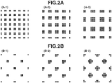
- Figs. 2A and 2B illustrate examples of the image patterns for evaluating the resolving power.
- the image patterns illustrated in Figs. 2A and 2B indicate image patterns at a writing resolution of 2400 dots per inch (dpi).
- the image pattern group illustrated in Fig. 2A is the group of the image patterns formed by performing the different halftone processing procedures on the predetermined tone data.
- Fig. 2A illustrates a group of image patterns (A-1) to (A-3) acquired by performing dither processing procedures corresponding to different screen rulings on image data having an image density of 25%.
- the screen rulings of (A-1), (A-2), and (A-3) are 600 line per inch (lpi), 400 lpi, and 300 lpi, respectively.
- a screen having the highest screen ruling used in the electrophotographic method inevitably varies depending on the machine type, but is often around 200 lpi in most cases. It is considered that this screen ruling is selected because the screen ruling that makes halftone dots unnoticeable in terms of human visual characteristics is around 200 lpi.
- the print result is more easily affected by the character resolution of the electrophotographic photosensitive member as described above.
- a density detection sensor that measures the densities of the test images (the toner images) formed from the image patterns for evaluating the resolving power will be described.
- An optical sensor including a pair of a light emission element and a light reception element can be suitably used as the density detection sensor. Light emitted from the light emission element is reflected by a surface of the formed test image, and reflected light therefrom is received by the light reception element.
- the density can be calculated from a light reception signal by tabling a relationship between the light reception signal and the density in advance.
- a location at which the density of the test image is measured may be a position on the electrophotographic photosensitive member, or may be a position on the intermediate transfer member or a position on the recording medium.
- measuring the density on the electrophotographic photosensitive member is a further desirable method because leading to an evaluation of the capability of the resolving power of the electrophotographic photosensitive member itself without being affected by a transfer process and processes subsequent thereto.
- the image data (A-1) having a high spatial frequency is first affected thereby and starts to output an unstable density, causing it to appear as a density difference from the image patterns (A-2) and (A-3). Comparing the measured density difference with the reference value allows the resolving power to be determined.
- Fig. 2A is assumed to use the three types of halftone processing, but the resolving power can be determined as long as at least two types of halftone processing are available.
- Fig. 2B is assumed to use the three types of halftone processing, but the resolving power can also be determined by using two types of halftone processing and referring to three points including the zero point.
- the resolving power of the electrophotographic photosensitive member is susceptible to the influence of the surface resistance on the electrophotographic photosensitive member.
- the surface resistance is affected by a material property of the surface of the electrophotographic photosensitive member or an attached substance on the surface of the electrophotographic photosensitive member. Therefore, the surface treatment of the electrophotographic photosensitive member according to the present exemplary embodiment is a treatment for removing the attached substance or a treatment for modifying the altered material property of the surface of the electrophotographic photosensitive member, such as a treatment of oxidizing the surface.
- examples of the method for removing the attached substance on the surface of the electrophotographic photosensitive member include a method that polishes the surface of the electrophotographic photosensitive member, such as a method discussed in the above-described patent literature, Japanese Patent Application Laid-Open No. 2010-122249 .
- a method that polishes the surface of the electrophotographic photosensitive member such as a method discussed in the above-described patent literature, Japanese Patent Application Laid-Open No. 2010-122249 .
- a method that polishes the surface of the electrophotographic photosensitive member such as a method discussed in the above-described patent literature, Japanese Patent Application Laid-Open No. 2010-122249 .
- a method that polishes the surface of the electrophotographic photosensitive member such as a method discussed in the above-described patent literature, Japanese Patent Application Laid-Open No. 2010-122249 .
- an electrophotographic photosensitive member in which the surface layer thereof is made of hydrogenated amorphous carbon containing less silicon elements to reduce the hydrophilicity of the surface layer and the surface resistance is controlled by applying the oxidation treatment on the outermost surface.
- Hydrogenated amorphous carbon has such a tendency that the sp 2 bond ratio increases and resistance reduces when a hydrogen amount reduces and a density of carbon atoms increases. Therefore, oxidizing the outermost surface made of hydrogenated amorphous carbon causes oxygen atoms to be bonded thereto, thereby being able to reduce the sp 2 bond ratio and enhance the surface resistance.
- the oxygen atoms bonded to the thus-modified outermost surface region are undesirably desorbed by being changed into CO 2 or CO in the long run, which may undesirably lead to an increase in the sp 2 bond ratio again and a reduction in the surface resistance, thereby undesirably resulting in a reduction in the surface resistance of the electrophotographic photosensitive member. Therefore, the resolving power can be recovered by applying the oxidation treatment on the surface of the electrophotographic photosensitive member in the electrophotographic apparatus when the resolving power of the electrophotographic photosensitive member reduces. More specifically, the outermost surface of the electrophotographic photosensitive member can be anodically oxidized by providing negative charges to the surface of the electrophotographic photosensitive member.
- this treatment can be realized just by carrying out an idle rotation, which repeats charges and discharges of the electrophotographic photosensitive member.
- the above-described treatment can be realized by supplying negative charges within a range that does not exceed voltage resistance of the electrophotographic photosensitive member and carrying out the idle rotation while discharging and charging the electrophotographic photosensitive member similarly to the negatively charging system. It is efficient to apply the oxidation treatment after separating a development unit, a cleaning unit, and the like in contact with the electrophotographic photosensitive member from the electrophotographic photosensitive member to complete the oxidation treatment in a further short time.
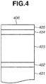
- Fig. 4 illustrates an example of a layer structure of the electrophotographic photosensitive member suitable for the present exemplary embodiment, and a lower blocking layer 402, a photoconductive layer 403, an intermediate layer 404, and a surface layer 405 are stacked on a conductive support substrate 401, and the surface layer 405 is made of hydrogenated amorphous carbon.
- an average value of a ratio of the number of hydrogen atoms (H) to a sum of the number of hydrogen atoms (H), the number of carbon atoms (C) and the number of silicon atoms (Si) (H/(H+C+Si)) of the surface layer is 0.40 or lower.
- the material of the surface layer of the electrophotographic photosensitive member especially suitable for the present exemplary embodiment is hydrogenated amorphous carbon. This is because the negative ions can be further prevented from being transmitted through the surface layer when the negative ions are provided to the electrophotographic photosensitive member, by achieving 0.40 or lower as a hydrogen content ratio of hydrogenated amorphous carbon forming the surface layer (the number of hydrogen atoms to a sum of the number of carbon atoms and the number of hydrogen atoms).
- the reduction in the hydrogen content ratio of the surface layer causes the increase in the bonds between the carbon atoms, thereby easily leading to an increase in the sp 2 bond ratio.
- the surface layer exhibits a characteristic closer to graphite, thereby easily reducing in electric resistance thereof.
- a factor affecting the image resolving power is surface resistance in the outermost surface region of the surface layer. This means that excellent image resolving power can be acquired by reducing the sp 2 bond ratio to 0.50 or lower in the outermost surface region of the surface layer.
- Examples of a method for controlling the sp 2 bond ratio in the outermost surface region of the surface layer include a method that modifies the property of the outermost surface region.
- One specific method is to apply a plasma treatment using treatment gas containing oxygen atoms to disassociate a ⁇ bond in the sp 2 bond in the outermost surface region and cause the oxygen atoms contained in the treatment gas containing the oxygen atoms to form an ether bond and ketone, by which the sp 2 bond ratio is considered to reduce as a result thereof.
- the treatment gas containing the oxygen atoms include oxygen (O 2 ), ozone (O 3 ), water vapor (H 2 O), carbon monoxide (CO), carbon dioxide (CO 2 ), and nitric oxide (NO).
- the intermediate layer is not limited in the electrophotographic photosensitive member suitable for the present exemplary embodiment, but the material thereof should be selected in consideration of an intermediary connection between the surface layer and the photoconductive layer.
- the material thereof should be selected in consideration of an intermediary connection between the surface layer and the photoconductive layer.
- hydrogenated amorphous silicon carbide can be desirably used as the material of the intermediate layer.
- Appropriately setting the composition of the a-SiC:H intermediate layer facilitates a movement of photocarriers generated in the photoconductive layer due to the exposure to the surface layer.
- Possible candidates for an atom for controlling conductivity include a so-called impurity in the semiconductor field. More specifically, usable atoms include an atom belonging to group 13 of the periodic table that provides positive (P-type) conductivity, or an atom belonging to group 15 of the periodic table that provides negative (N-type) conductivity. Among the atoms belonging to group 13 of the periodic table, the boron atom, the aluminum atom, and the gallium atom are desirable. Among the atoms belonging to group 15 of the periodic table, the phosphorus atom and the arsenic atom are desirable.
- the photoconductive layer may be formed by a single layer, or may be formed by a plurality of layers (for example, a charge generation layer and a charge transport layer).
- a substrate 3112 connected to the earth, a substrate heating heater 3113, and a material gas introduction tube 3114 are set up in the reaction container 3110 in the deposition device 3100. Further, a high-frequency electric power source 3120 is connected to a cathode electrode 3111 via a high-frequency matching box 3115.
- the substrate 3112 degreased and washed in advance is set in the reaction container 3110 via a holding table 3123.
- the exhaust device (not illustrated) is driven and the reaction container 3110 is evacuated.
- a predetermined pressure such as 1 Pa or lower with a display of a vacuum meter 3119 under observation
- electric power is supplied to the substrate heating heater 3113 and the substrate 3112 is heated to a predetermined temperature of 50 to 350 °C.
- the substrate 3122 can also be heated under an inert gas atmosphere by supplying inert gas such as argon (Ar) and helium (He) from the gas supply device 3200 into the reaction container 3110.
- the following gas can be used as the material gas for supplying the carbon atoms to form the surface layer made of hydrogenated amorphous carbon.
- Desirably usable examples include methane (CH 4 ), ethane (C 2 H 6 ), propane (C 3 H 8 ), butane (C 4 H 10 ), ethylene (C 2 H 4 ), and acethylene (C 2 H 2 ).
- the outermost surface region of the surface layer made of hydrogenated amorphous carbon can be processed as intended by applying the plasma treatment thereon using gas containing oxygen atoms.
- silanes such as silane (SiH 4 ) and disilane (Si 2 H 6 ) can be desirably used as the material gas for supplying silicon atoms to form the intermediate layer made of hydrogenated amorphous silicon carbide.
- the intermediate layer is formed by setting the conditions such as the flow rate of the material gas to be supplied into the reaction container 3110, the high-frequency electric power, the pressure in the reaction container 3110, and the temperature of the substrate 3112 as necessary.
- the charge injection blocking power can be provided to the intermediate layer by forming the intermediate layer while adding the material gas containing the atom belonging to group 13 or group 15 of the periodic table according to the charging polarity.
- the material gas containing the atom belonging to group 13 or group 15 of the periodic table include phosphine (PH 3 ) and diborane (B 2 H 6 ).
- silanes such as silane (SiH 4 ) and disilane (Si 2 H 6 ) can be desirably used as the material gas for supplying silicon atoms to form the photoconductive layer made of hydrogenated amorphous silicon.
- silanes such as silane (SiH 4 ) and disilane (Si 2 H 6 ) can be desirably used as the material gas for supplying silicon atoms to form the photoconductive layer made of hydrogenated amorphous silicon.
- hydrogen (H 2 ) can also be desirably used in addition to the above-described silanes as the material gas for supplying hydrogen atoms.
- halogen atom, atom for controlling the conductivity, carbon atom, oxygen atom, nitrogen atom, and the like are put into the photoconductive layer, this can be realized by using a gaseous substance or a substance easily transformable into gas that contains each of the atoms as a material as appropriate.
- the electrophotographic method according to the present exemplary embodiment was applied to an apparatus converted from a digital electrophotographic apparatus "imagePRESS C65" (trade name) manufactured by Canon, Incorporated.
- the electrophotographic apparatus was equipped with a determination unit configured to store the reference value defined based on the relationship between the area coverage modulation data of the patch and the measured density data and determine the resolving power from the measured density data.
- the resolving power was evaluated using the patch patterns illustrated in Fig. 2A . Since the patch patterns illustrated in Fig. 2A are patch patterns corresponding to the same area coverage modulation and the different rulings, the determination about the resolving power is defined based on the density difference among the individual patches, and the resolving power of the electrophotographic photosensitive member can be determined to be higher as the density difference among the individual patches reduces.
- the electrophotographic apparatus was a system using the electrophotographic photosensitive member including the surface layer made of hydrogenated amorphous carbon and configured to negatively charge the electrophotographic photosensitive member
- the oxidation treatment was applied as the surface treatment of the electrophotographic photosensitive member. More specifically, the idle rotation was carried out by repeatedly charging and discharging the electrophotographic photosensitive member.
- a table 1 indicates electrophotographic photosensitive members used in the present example and the present comparative example, and the conditions.
- the image resolving power was evaluated by using the apparatus converted from the digital electrophotographic apparatus "imagePRESS C65" (trade name) manufactured by Canon, Incorporated.
- the converted apparatus was configured to allow primary charging and a development bias to be applied from an external electric power source.
- the resolution of the output image was evaluated based on an area coverage modulation image by using a halftone dot screen having the highest screen ruling of 230 lpi mounted on the main body.
- Tone data evenly divided into 17 stages was used as the area coverage modulation image. At this time, a number was assigned to each of the tones with 16 assigned to the darkest tone and 0 assigned to the lightest tone, and was defined to indicate a tone stage.
- the image density was measured by using a reflection densitometer (504 Spectro-densitometer manufactured by X-Rite, Incorporated) for each of 0 to 8 tones.
- a reflection densitometer 504 Spectro-densitometer manufactured by X-Rite, Incorporated
- three images were output for each of the tones and an average value of densities thereof was set as an evaluation value.
- a value of a determination coefficient R2 at the time of linear approximation of the thus-acquired evaluation value and the tone stage was calculated, and a result thereof was evaluated with 0.996 or higher as A, 0.990 or higher and lower than 0.996 as B, and a value lower than 0.990 as C.
- the result evaluated as B or higher was determined to be able to acquire the effect of the present exemplary embodiment.
- a table 4 indicates the electrophotographic photosensitive members used in the present example, and the conditions. The same conditions as the example 1 were employed as the evaluation method and criteria. The present example was different in terms of use of the patch patterns illustrated in Fig. 2B as the image patterns of the test images for determining the resolving power of the electrophotographic photosensitive member.
- the resolving power of the electrophotographic photosensitive member can be accurately detected during the non-image formation period, and the resolving power of the electrophotographic photosensitive member can be recovered by applying the surface treatment on the electrophotographic photosensitive member as necessary. As a result, the original performance of the electrophotographic apparatus can be maintained.
- a method for controlling an electrophotographic apparatus including forming a first measurement image by performing first halftone processing on image data, forming a second measurement image by performing second halftone processing different from the first halftone processing on the image data, measuring densities of the first measurement image and the second measurement image, calculating a density difference between each of densities of the measurement images, determining whether the density difference satisfies a predetermined reference value, and applying a surface treatment on an electrophotographic photosensitive member if the density difference does not satisfy the reference value, during a non-image formation period.
Landscapes
- Physics & Mathematics (AREA)
- General Physics & Mathematics (AREA)
- Engineering & Computer Science (AREA)
- Microelectronics & Electronic Packaging (AREA)
- Life Sciences & Earth Sciences (AREA)
- Sustainable Development (AREA)
- Sustainable Energy (AREA)
- Photoreceptors In Electrophotography (AREA)
- Control Or Security For Electrophotography (AREA)
Applications Claiming Priority (1)
| Application Number | Priority Date | Filing Date | Title |
|---|---|---|---|
| JP2019036834A JP2020140127A (ja) | 2019-02-28 | 2019-02-28 | 電子写真装置の制御方法 |
Publications (2)
| Publication Number | Publication Date |
|---|---|
| EP3702843A2 true EP3702843A2 (de) | 2020-09-02 |
| EP3702843A3 EP3702843A3 (de) | 2020-11-25 |
Family
ID=69740116
Family Applications (1)
| Application Number | Title | Priority Date | Filing Date |
|---|---|---|---|
| EP20158786.2A Withdrawn EP3702843A3 (de) | 2019-02-28 | 2020-02-21 | Verfahren zur steuerung einer elektrofotografischen vorrichtung |
Country Status (3)
| Country | Link |
|---|---|
| US (1) | US10976682B2 (de) |
| EP (1) | EP3702843A3 (de) |
| JP (1) | JP2020140127A (de) |
Families Citing this family (1)
| Publication number | Priority date | Publication date | Assignee | Title |
|---|---|---|---|---|
| WO2021071501A1 (en) * | 2019-10-11 | 2021-04-15 | Hewlett-Packard Development Company, L.P. | Correction for low gray coverage printing |
Citations (2)
| Publication number | Priority date | Publication date | Assignee | Title |
|---|---|---|---|---|
| JP3030975B2 (ja) | 1991-10-04 | 2000-04-10 | 松下電器産業株式会社 | 画質制御装置 |
| JP2010122249A (ja) | 2008-11-17 | 2010-06-03 | Kyocera Mita Corp | 画像形成装置 |
Family Cites Families (16)
| Publication number | Priority date | Publication date | Assignee | Title |
|---|---|---|---|---|
| JP2002131958A (ja) * | 2000-10-25 | 2002-05-09 | Canon Inc | 画像形成装置 |
| JP2002174915A (ja) * | 2000-12-06 | 2002-06-21 | Canon Inc | 画像形成装置 |
| US6768878B2 (en) * | 2001-10-30 | 2004-07-27 | Konica Corporation | Image forming method and image forming apparatus utilizing a control patch |
| JP4214699B2 (ja) * | 2002-01-15 | 2009-01-28 | コニカミノルタホールディングス株式会社 | 画像形成方法および画像形成装置 |
| JP2003337455A (ja) * | 2002-05-21 | 2003-11-28 | Canon Inc | 画像濃度検出装置及びこれを用いた画像濃度制御装置 |
| JP2005017607A (ja) * | 2003-06-25 | 2005-01-20 | Fuji Xerox Co Ltd | 光ビーム走査装置、及びそれを備えた画像形成装置 |
| JP2008310311A (ja) * | 2007-05-17 | 2008-12-25 | Ricoh Co Ltd | 画像形成装置、画像形成方法及びプロセスカートリッジ |
| JP2012083588A (ja) * | 2010-10-13 | 2012-04-26 | Konica Minolta Business Technologies Inc | 画像形成装置 |
| JP2012185257A (ja) * | 2011-03-04 | 2012-09-27 | Konica Minolta Business Technologies Inc | 像流れ検知装置及び画像形成装置 |
| JP6208429B2 (ja) * | 2013-01-18 | 2017-10-04 | キヤノンファインテックニスカ株式会社 | 画像形成装置 |
| JP2014137551A (ja) * | 2013-01-18 | 2014-07-28 | Canon Finetech Inc | 画像形成装置 |
| JP6154762B2 (ja) | 2014-02-20 | 2017-06-28 | 京セラドキュメントソリューションズ株式会社 | 画像流れ検出装置及び画像形成装置 |
| JP2015166820A (ja) * | 2014-03-04 | 2015-09-24 | コニカミノルタ株式会社 | 画像形成装置 |
| WO2016068036A1 (ja) * | 2014-10-31 | 2016-05-06 | 京セラドキュメントソリューションズ株式会社 | 画像形成装置、その画像形成装置に使用される現像剤、及び画像形成方法 |
| JP2018025714A (ja) * | 2016-08-12 | 2018-02-15 | キヤノン株式会社 | 電子写真感光体 |
| JP2017187795A (ja) | 2017-06-16 | 2017-10-12 | キヤノンファインテックニスカ株式会社 | 画像形成装置 |
-
2019
- 2019-02-28 JP JP2019036834A patent/JP2020140127A/ja active Pending
-
2020
- 2020-02-21 EP EP20158786.2A patent/EP3702843A3/de not_active Withdrawn
- 2020-02-25 US US16/801,057 patent/US10976682B2/en active Active
Patent Citations (2)
| Publication number | Priority date | Publication date | Assignee | Title |
|---|---|---|---|---|
| JP3030975B2 (ja) | 1991-10-04 | 2000-04-10 | 松下電器産業株式会社 | 画質制御装置 |
| JP2010122249A (ja) | 2008-11-17 | 2010-06-03 | Kyocera Mita Corp | 画像形成装置 |
Also Published As
| Publication number | Publication date |
|---|---|
| US10976682B2 (en) | 2021-04-13 |
| US20200278620A1 (en) | 2020-09-03 |
| EP3702843A3 (de) | 2020-11-25 |
| JP2020140127A (ja) | 2020-09-03 |
Similar Documents
| Publication | Publication Date | Title |
|---|---|---|
| US8173344B2 (en) | Electrophotographic photosensitive member and electrophotographic apparatus | |
| EP2148245B1 (de) | Elektrofotografisches lichtempfindliches Element und elektrofotografische Vorrichtung | |
| US8168365B2 (en) | Method for manufacturing electrophotographic photosensitive member | |
| US10976682B2 (en) | Method for controlling electrophotographic apparatus | |
| US7157197B2 (en) | Electrophotographic photosensitive member | |
| JP4775938B2 (ja) | 電子写真用感光体の形成方法 | |
| US8440377B2 (en) | Electrophotographic photosensitive member and electrophotographic apparatus | |
| EP2328031B1 (de) | Elektrofotografisches lichtempfindliches Element und elektrofotografische Vorrichtung | |
| JP3181165B2 (ja) | 光受容部材 | |
| EP2422239B1 (de) | Elektrofotografisches lichtempfindliches element und elektrofotografische vorrichtung damit | |
| JP2006133525A (ja) | 電子写真感光体及びこれを用いた電子写真装置 | |
| EP2813894A1 (de) | Elektrofotografisches lichtempfindliches Element und elektrofotografische Vorrichtung | |
| US8088543B2 (en) | Electrophotographic photosensitive member and electrophotographic apparatus | |
| JP6808541B2 (ja) | 電子写真感光体 | |
| JP3229002B2 (ja) | 電子写真用光受容部材 | |
| JP4683637B2 (ja) | 電子写真感光体および電子写真装置 | |
| JP2020122840A (ja) | 電子写真装置の制御方法 | |
| JP2006133522A (ja) | 電子写真感光体 | |
| JP2536733B2 (ja) | 光受容部材 | |
| JP3420385B2 (ja) | 堆積膜形成装置及び堆積膜形成方法 | |
| JP2020122841A (ja) | 電子写真装置の制御方法 | |
| JP2020071276A (ja) | 画像形成方法 | |
| JP2006133524A (ja) | 電子写真感光体および電子写真装置 | |
| JP2006189823A (ja) | 電子写真感光体 | |
| JPS58149055A (ja) | 光導電部材 |
Legal Events
| Date | Code | Title | Description |
|---|---|---|---|
| PUAI | Public reference made under article 153(3) epc to a published international application that has entered the european phase |
Free format text: ORIGINAL CODE: 0009012 |
|
| STAA | Information on the status of an ep patent application or granted ep patent |
Free format text: STATUS: THE APPLICATION HAS BEEN PUBLISHED |
|
| AK | Designated contracting states |
Kind code of ref document: A2 Designated state(s): AL AT BE BG CH CY CZ DE DK EE ES FI FR GB GR HR HU IE IS IT LI LT LU LV MC MK MT NL NO PL PT RO RS SE SI SK SM TR |
|
| AX | Request for extension of the european patent |
Extension state: BA ME |
|
| PUAL | Search report despatched |
Free format text: ORIGINAL CODE: 0009013 |
|
| AK | Designated contracting states |
Kind code of ref document: A3 Designated state(s): AL AT BE BG CH CY CZ DE DK EE ES FI FR GB GR HR HU IE IS IT LI LT LU LV MC MK MT NL NO PL PT RO RS SE SI SK SM TR |
|
| AX | Request for extension of the european patent |
Extension state: BA ME |
|
| RIC1 | Information provided on ipc code assigned before grant |
Ipc: G03G 15/01 20060101ALI20201016BHEP Ipc: G03G 15/04 20060101ALN20201016BHEP Ipc: G03G 15/00 20060101AFI20201016BHEP |
|
| STAA | Information on the status of an ep patent application or granted ep patent |
Free format text: STATUS: REQUEST FOR EXAMINATION WAS MADE |
|
| 17P | Request for examination filed |
Effective date: 20210525 |
|
| RBV | Designated contracting states (corrected) |
Designated state(s): AL AT BE BG CH CY CZ DE DK EE ES FI FR GB GR HR HU IE IS IT LI LT LU LV MC MK MT NL NO PL PT RO RS SE SI SK SM TR |
|
| STAA | Information on the status of an ep patent application or granted ep patent |
Free format text: STATUS: THE APPLICATION HAS BEEN WITHDRAWN |
|
| RIC1 | Information provided on ipc code assigned before grant |
Ipc: G03G 15/04 20060101ALN20230202BHEP Ipc: G03G 15/01 20060101ALI20230202BHEP Ipc: G03G 15/00 20060101AFI20230202BHEP |
|
| 18W | Application withdrawn |
Effective date: 20230213 |