EP3675607A2 - Verdrahtungssubstrat und verfahren zur herstellung davon - Google Patents
Verdrahtungssubstrat und verfahren zur herstellung davon Download PDFInfo
- Publication number
- EP3675607A2 EP3675607A2 EP19219851.3A EP19219851A EP3675607A2 EP 3675607 A2 EP3675607 A2 EP 3675607A2 EP 19219851 A EP19219851 A EP 19219851A EP 3675607 A2 EP3675607 A2 EP 3675607A2
- Authority
- EP
- European Patent Office
- Prior art keywords
- portions
- substrate
- curved portions
- view
- plan
- Prior art date
- Legal status (The legal status is an assumption and is not a legal conclusion. Google has not performed a legal analysis and makes no representation as to the accuracy of the status listed.)
- Withdrawn
Links
Images


Classifications
-
- H—ELECTRICITY
- H10—SEMICONDUCTOR DEVICES; ELECTRIC SOLID-STATE DEVICES NOT OTHERWISE PROVIDED FOR
- H10W—GENERIC PACKAGES, INTERCONNECTIONS, CONNECTORS OR OTHER CONSTRUCTIONAL DETAILS OF DEVICES COVERED BY CLASS H10
- H10W70/00—Package substrates; Interposers; Redistribution layers [RDL]
- H10W70/60—Insulating or insulated package substrates; Interposers; Redistribution layers
- H10W70/67—Insulating or insulated package substrates; Interposers; Redistribution layers characterised by their insulating layers or insulating parts
- H10W70/68—Shapes or dispositions thereof
-
- H—ELECTRICITY
- H05—ELECTRIC TECHNIQUES NOT OTHERWISE PROVIDED FOR
- H05K—PRINTED CIRCUITS; CASINGS OR CONSTRUCTIONAL DETAILS OF ELECTRIC APPARATUS; MANUFACTURE OF ASSEMBLAGES OF ELECTRICAL COMPONENTS
- H05K3/00—Apparatus or processes for manufacturing printed circuits
- H05K3/0011—Working of insulating substrates or insulating layers
- H05K3/0044—Mechanical working of the substrate, e.g. drilling or punching
- H05K3/0052—Depaneling, i.e. dividing a panel into circuit boards; Working of the edges of circuit boards
-
- H—ELECTRICITY
- H10—SEMICONDUCTOR DEVICES; ELECTRIC SOLID-STATE DEVICES NOT OTHERWISE PROVIDED FOR
- H10W—GENERIC PACKAGES, INTERCONNECTIONS, CONNECTORS OR OTHER CONSTRUCTIONAL DETAILS OF DEVICES COVERED BY CLASS H10
- H10W99/00—Subject matter not provided for in other groups of this subclass
-
- H—ELECTRICITY
- H05—ELECTRIC TECHNIQUES NOT OTHERWISE PROVIDED FOR
- H05K—PRINTED CIRCUITS; CASINGS OR CONSTRUCTIONAL DETAILS OF ELECTRIC APPARATUS; MANUFACTURE OF ASSEMBLAGES OF ELECTRICAL COMPONENTS
- H05K1/00—Printed circuits
- H05K1/02—Details
- H05K1/03—Use of materials for the substrate
- H05K1/0306—Inorganic insulating substrates, e.g. ceramic, glass
-
- H—ELECTRICITY
- H05—ELECTRIC TECHNIQUES NOT OTHERWISE PROVIDED FOR
- H05K—PRINTED CIRCUITS; CASINGS OR CONSTRUCTIONAL DETAILS OF ELECTRIC APPARATUS; MANUFACTURE OF ASSEMBLAGES OF ELECTRICAL COMPONENTS
- H05K2201/00—Indexing scheme relating to printed circuits covered by H05K1/00
- H05K2201/09—Shape and layout
- H05K2201/09009—Substrate related
- H05K2201/09027—Non-rectangular flat PCB, e.g. circular
-
- H—ELECTRICITY
- H05—ELECTRIC TECHNIQUES NOT OTHERWISE PROVIDED FOR
- H05K—PRINTED CIRCUITS; CASINGS OR CONSTRUCTIONAL DETAILS OF ELECTRIC APPARATUS; MANUFACTURE OF ASSEMBLAGES OF ELECTRICAL COMPONENTS
- H05K2201/00—Indexing scheme relating to printed circuits covered by H05K1/00
- H05K2201/09—Shape and layout
- H05K2201/09009—Substrate related
- H05K2201/09063—Holes or slots in insulating substrate not used for electrical connections
-
- H—ELECTRICITY
- H05—ELECTRIC TECHNIQUES NOT OTHERWISE PROVIDED FOR
- H05K—PRINTED CIRCUITS; CASINGS OR CONSTRUCTIONAL DETAILS OF ELECTRIC APPARATUS; MANUFACTURE OF ASSEMBLAGES OF ELECTRICAL COMPONENTS
- H05K3/00—Apparatus or processes for manufacturing printed circuits
- H05K3/46—Manufacturing multilayer circuits
- H05K3/4611—Manufacturing multilayer circuits by laminating two or more circuit boards
- H05K3/4626—Manufacturing multilayer circuits by laminating two or more circuit boards characterised by the insulating layers or materials
- H05K3/4629—Manufacturing multilayer circuits by laminating two or more circuit boards characterised by the insulating layers or materials laminating inorganic sheets comprising printed circuits, e.g. green ceramic sheets
Definitions
- the present invention relates to a wiring substrate whose outline, in plan view, has a particular shape, for example, a circular shape, and to a method of manufacturing the wiring substrate.
- a ceramic substrate body of a ceramic wiring substrate has a circular outline in plan view
- blanking is performed on a ceramic green sheet from which the above-mentioned substrate body will be obtained later.
- the blanking is performed through use of a circular columnar punch, and a die having a receiving hole for receiving a distal end portion of the punch.
- the center axis of the punch and the center axis of the die deviate from each other, it is difficult to blank out the substrate body from the ceramic green sheet such that the substrate body has a true circular shape in plan view.
- the distal end portion of the punch is deformed or broken, huge cost is needed for renewal of the punch. Therefore, there have been problems in terms of productivity and economy.
- a ceramic substrate manufacturing method which solves the above-described problems has been proposed (see, for example, Patent Document 1).
- a plurality of product regions having a circular outline in plan view are formed on an unfired green ceramic compact (mother substrate) such that the product regions are separated from one another; the green ceramic compact having the product regions is fired; subsequently, a resultant fired ceramic plate is divided into a plurality of pieces respectively including the plurality of product regions and respective throwaway regions surrounding the circumferences of the product regions and each having a polygonal (e.g., octagonal) outline in plan view; and the throwaway regions are successively ground from their peripheral sides by using a grinding stone such that disc-shaped ceramic substrates are formed.
- a polygonal e.g., octagonal
- the above-described ceramic substrate manufacturing method requires a complex cutting step of obtaining ceramic sintered bodies each composed of the above-mentioned product region and the throwaway region surrounding the circumference thereof, and a grinding step of subsequently pressing the throwaway region of each ceramic sintered body against the circumferential surface of a rotating grinding stone such that the outer periphery of the throwaway region comes into contact with the circumferential surface of a rotating grinding stone, thereby grinding the throwaway region. Therefore, the above-described ceramic substrate manufacturing method has the following problems. First, since the circularity in plan view is likely to vary among obtained ceramic substrates, stabilization of shape and dimensional accuracy is difficult. Second, since ceramic sintered bodies generally are high in hardness and excellent in wear resistance, the above-mentioned grinding step requires a very long time.
- Patent Document 1 is Japanese Patent Application Laid-Open ( kokai ) No. 2001-68599 (pages 1 to 6 and FIGS. 1 to 7 ) .
- An object of the present invention is to provide a wiring substrate which is stable in shape and dimensional accuracy despite that its substrate body formed of an insulating material has a circular shape or the like shape in plan view.
- Another object of the present invention is to provide a manufacturing method which can quickly manufacture such a wiring substrate by a relatively small number of simple steps.
- the present invention has been accomplished on the basis of the idea of defining a product outline in plan view of the substrate body formed of an insulating material by a plurality of curved portions separated from one another and a plurality of straight portions each located between adjacent ones of the curved portions, and specifying the total length of the curved portions.
- a wiring substrate of the present invention comprises a substrate body formed of an insulating material and having a front surface and a back surface and having a side surface located between the front surface and the back surface, wherein, in a plan view which is a view from the front surface side, an outline of the substrate body includes a plurality of curved portions separated from one another and a plurality of straight portions each located between adjacent ones of the plurality of curved portions, and wherein, in the plan view, the total length of the plurality of curved portions is at least 40% of the sum of the total length of the plurality of curved portions and the total length of the straight portions.
- the reason why the total length of the plurality of curved portions is specified to be at least 40% of the sum is to exclude substrate bodies having known shapes; for example, a substrate body which has a quadrangular (square or rectangular) outline in plan view and outwardly convex curved (radiused) portions at four corners.
- the wiring substrate as described yields the following effects (1) and (2).
- the ratio of the total length of the plurality of curved portions to the sum of the total length of the plurality of curved portions and the total length of the plurality of straight portions is preferably 40% to 70%, more preferably, 60% to 65%.
- the wiring substrate can have sufficiently long curved portions while having straight portions.
- the insulating material is a ceramic material (e.g., alumina) or a resin (e.g., epoxy resin).
- the substrate body may be composed of a single insulating layer, or a plurality of insulating layers stacked together.
- the single insulating layer has appropriate connection conductors individually formed on each of the front and back surfaces, and via conductors extending through the insulating layer and establishing electrical continuity between the connection conductors on the front surface and the connection conductors on the back surface.
- inner layer wiring conductors are formed between the insulating layers.
- the shape of the curved portions may be a curve defined by a single center and a single radius from the center (axis) or a curve (for example, a portion of an ellipse or a portion of a cycloid curve) defined by a plurality of centers and a plurality or radiuses from the centers (axes).
- the substrate body may have an open cavity or open cavities formed on at least one of the front surface and the back surface, or an additional through hole(s) extending between the front surface and the back surface.
- the present invention encompasses a wiring substrate in which, in the plan view, the plurality of curved portions correspond to a plurality of portions of an imaginary true circle, an imaginary ellipse, or an imaginary elongated circle which represents a product outline.
- the plurality of curved portions forming the outline of the substrate body in plan view form a plurality of portions of an imaginary true circle, an imaginary ellipse, or an imaginary elongated circle which are product outlines. Therefore, the wiring substrate has a substrate body having an outline which is identical with any of the product outlines or is very similar in shape to any of the product outlines. Accordingly, the above-described effect can be obtained actuality.
- the present invention encompasses a wiring substrate in which, in the plan view, each straight portion is located outward in relation to ends of the curved portions located on opposite sides of the straight portion, the ends of the curved portions being located adjacent to the straight portion.
- the substrate body in plan view, the substrate body contains the product outline without fail. Therefore, the above-described effect (1) can be obtained more reliably.
- handling e.g., transportation
- the above-described effect (2) can be obtained reliably.
- each straight portion may be located slightly inward of ends of the curved portions located on opposite sides of the straight portion, the ends being located adjacent to the straight portion.
- the present invention encompasses a wiring substrate in which the substrate body is composed of a plurality of insulating layers stacked together, and at least one of the insulating layers has (defines) recesses which are formed at the straight portions and are open toward an outside of the straight portions in the plan view.
- FIG. 1A is a plan view of a wiring substrate 1a according to a first embodiment of the present invention
- FIG. 1B is a vertical sectional view of the wiring substrate 1a taken along line B-B in FIG. 1A .
- the wiring substrate 1a includes a substrate body 2a composed of a plurality of ceramic (insulating material) layers c1 to c3 stacked together.
- the substrate body 2a has a front surface 3a and a back surface 4a located on opposite sides thereof, and has a side surface located between the front surface 3a and the back surface 4a.
- the outline of the substrate body 2a in plan view from the front surface 3a side has four (a plurality of) curved portions R1 and four (a plurality of) straight portions 5.
- the curved portions R1 are separated from one another, and each of the straight portions 5 is located between two adjacent ones of the curved portions R1.
- the ceramic layers c1 to c3 are formed mainly of, for example, alumina.
- the four curved portions R1 constitute a plurality of portions of an imaginary true circle S1 which is an imaginary product outline of the front surface 3a and are disposed at positions which are point symmetry with one another with respect to the center of the true circle S1.
- each straight portion 5 located between two adjacent ones of the curved portions R1 is located outward of end portions of the curved portions R1 on the opposite sides of the straight portion 5, the end portions being located adjacent to the straight portion 5, and a portion of the true circle S1 is tangent to a longitudinal central portion of the straight portion 5.
- the four straight portions 5 are also disposed at positions which are point symmetry with one another with respect to the center of the true circle S1.
- the total length of the four curved portions R1 accounts for about 50% (40% or more) of the sum of the total length of the four curved portions R1 and the total length of the four straight portions 5.
- a plurality of electrode pads 6 and a plurality of electrode pads 7 are formed on the front surface 3a of the substrate body 2a.
- the electrode pads 6 are disposed in a lattice pattern in a central region of the front surface 3a.
- the electrode pads 7 are disposed in a ring-shaped pattern at approximately equal intervals along the periphery of the front surface 3a; i.e., along the imaginary true circle S1.
- a plurality of external connection terminals 9 are formed on the back surface 4a of the substrate body 2a.
- the external connection terminals 9 are electrically connected to the electrode pads 6 and 7 formed on the front surface 3a through via conductors 8 penetrating the ceramic layers c1 to c3 at predetermined positions and a plurality of unillustrated inner layer wiring conductors formed between the ceramic layers c1 to c3.
- the electrode pads 6 and 7, the via conductors 8, the external connection terminals 9, and the inner layer wiring conductors are formed mainly of tungsten (W) or molybdenum (Mo).
- the lowermost ceramic layer c3 has recesses 10 which are formed approximately at the longitudinal centers of the straight portions 5 and which have a rectangular shape in plan view and are open outward.
- an electronic component such as a semiconductor device is mounted on the electrode pads 6 and 7, the recesses 10 are utilized; i.e., jigs (not shown) for positioning the substrate body 2a are fitted into the recesses 10.
- the recesses 10 may be formed along the entire length of the substrate body 2a in the thickness direction thereof; i.e., between the front surface 3a and the back surface 4a.
- the plan view of the back surface 4a of the substrate body 2a is the same as that of the front surface 3a except that the back surface 4a has the recesses 10.
- FIGS. 2A and 2B are plan views showing a wiring substrate 1a' and a wiring substrate 1a" which are modifications of the wiring substrate 1a.
- the electrode pads 6 and 7 are not illustrated in these drawings.
- the outline of the wiring substrate 1a' has two curved portions R2 as portions of the imaginary true circle S1 and two straight portions 5 located between the curved portions R2.
- the outline of the wiring substrate 1a" has three curved portions R3 as portions of the imaginary true circle S1 and three straight portions 5 each located between adjacent ones of the curved portions R3.
- the total length of the two curved portions R2 of the wiring substrate 1a' accounts for about 60% (40% or more) of the sum of the total length of the two curved portions R2 and the total length of the two straight portions 5.
- the total length of the three curved portions R3 of the wiring substrate 1a" accounts for about 70% (40% or more) of the sum of the total length of the three curved portions R3 and the total length of the three straight portions 5.
- the recesses 10 may be formed at the straight portions 5 of the wiring substrates 1a' and 1a" in a manner similar to the above-described manner.
- the total length of the curved portions R1 to R3 of the outline of the substrate body 2a in plan view accounts for at least 40% of the sum of the total length of the curved portions R1 to R3 and the total length of the straight portions 5. Therefore, for example, even when the outline of the substrate body 2a in plan view is rendered similar to a circular shape, the degree of freedom of design can be increased, and an error produced in its manufacturing process can be absorbed more easily. Therefore, it is possible to provide the wiring substrate 1a which is high in accuracy and whose shape and dimensions are as close as possible to the shape and dimensions of the required true circle S1. Also, since the straight portions 5 remain as parts of the outline of the substrate body 2a, it is possible to obtain the generally circular wiring substrate 1a whose direction and posture can be easily recognized.
- each of the straight portions 5 has the recess 10 which is open toward the outside with respect to the straight portion 5 (reference). Therefore, when an electronic component is mounted on the front surface 3a of the substrate body 2a, positioning jigs can be fitted into the recesses 10. Also, a side surface conductor having a concave shape or a like shape in plan view can be accurately disposed on a side surface of the substrate body 2a such that the side surface conductor extends over a portion or the entirety (entire length) of the side surface in the thickness direction.
- the wiring substrate 1a can yield the above-described effects (1) to (3) without fail.
- a method of manufacturing the wiring substrate 1a will now be described with reference to FIGS. 3A to 3H .
- a ceramic slurry was prepared beforehand by mixing alumina powder, a binder resin, a solvent, a plasticizer, etc., in respective proper amounts. The ceramic slurry was then formed into a sheet shape by a doctor blade method. Thus, a mother substrate Gn (a ceramic green sheet for multiple pieces) was manufactured. As shown in FIG. 3A , the mother substrate Gn had a front surface 3A and a back surface 4A located on opposite sides thereof. Notably, the mother substrate Gn may be formed of three green sheets stacked together or a single green sheet. Such a mother substrate Gn continuously extends in the vertical direction toward the lower side of FIG. 3A (this holds true in the following description).
- Green (unfired) conductive layers which were to become the electrode pads 6 and 7, the via conductors 8, the external connection terminals 9, and the inner layer wiring conductors, respectively, were formed beforehand on the green sheet at predetermined positions.
- an imaginary true circle (imaginary product outline) S1 was set on the mother substrate Gn at each of predetermined positions. Subsequently, a blanking step for forming the curved portions R1 was performed at four positions which were located on the outer side of the true circle S1 and along the true circle S1 and were point symmetry with one another with respect to the center of the true circle S1.
- the blanking step was performed by using a punch P1 and a die D1 shown in FIGS. 3C and 3D , respectively.
- the punch P1 has a distal end surface 11 including a concave curved surface r1 similar in shape to the curved portion R1.
- the die D1 has a receiving hole 12 which receives a distal end portion of the punch P1 and which includes a convex curved surface r1 similar in shape to the curved portion R1.
- the die D1 was disposed on the back surface 4A side of the mother substrate Gn. Subsequently, the punch P1 was moved downward on the front surface 3A side of the mother substrate Gn such that the distal end portion of the punch P1 penetrated the mother substrate Gn and entered the receiving hole 12 of the die D1.
- this blanking process may be performed simultaneously at the above-described four positions or performed sequentially position by position.
- the blanking process for forming the curved portions R1 be performed sequentially position by position.
- the mother substrate Gn was fired, and a cutting step was then performed.
- a disc-shaped cutter rotating at high speed was caused to pass along each of imaginary cutting lines located on the outer side of the true circle S1 and each extending between two curved portions R1 located in two adjacent ones of the through holes 14.
- the above-described wiring substrate 1a was obtained.
- the outline of the substrate body 2a is formed by the four curved portions R1 which are point symmetry with one another with respect to the center of the imaginary true circle S1 and the four straight portions 5 each of which is located between two adjacent ones of the curved portions R1 and which are located on the outer side of the true circle S1 to be point symmetry with one another with respect to the center of the imaginary true circle S1.
- the above-mentioned cutter may be caused to pass along each of imaginary cutting lines located slightly inward of the true circle S1 and each extending between two curved portions R1 located in two adjacent ones of the through holes 14.
- the straight portions 5 are formed to be located slightly inward of the true circle S1.
- a blanking process may be performed, at each midpoint between two adjacent ones of the through holes 14, through use of a punch 15 and a die 16.
- the punch 15 has a rectangular parallelepiped shape as a whole and has a rectangular (quadrangular) distal end surface
- the die 16 has a receiving hole for receiving a distal end portion of the punch 15.
- rectangular through holes 18 were individually formed at a position near the midpoint between two adjacent ones of the through holes 14.
- the through hole 18 extends in the radial direction of the true circle S1 and intersects with the true circle S1.
- the plurality of curved portions R1 of the substrate body 2a (serving to form the outline in plan view) were formed by using the punch P1 having the concave curved surface r1 for forming the curved portion R1 and the die D1 having the receiving hole 12 including the convex curved surface r1 similar in shape to the above-mentioned concave curved surface r1.
- the substrate body 2a had not yet been separated from the mother substrate Gn.
- the mother substrate Gn was cut along imaginary cutting lines each located between two adjacent ones of the curved portions R1; i.e., along portions of the mother substrate Gn becoming the straight portions 5 of the substrate body 2a. As a result, all the side surfaces of the substrate body 2a was formed accurately within a relatively short time.
- the punch P1 and the die D1 have the concave curved surface r1 and the convex curved surface r1, respectively, which correspond to the curved portion R1. Therefore, the punch P1 and the die D1 are relatively small in size and can be manufacture easily at low cost. In addition, when the punch P1 and/or the die D1 wears, deforms, or breaks, the punch P1 and/or the die D1 can be repaired or replaced with a new one within a short period or time and at low cost. Therefore, facility cost and time and effort of facility management can be reduced, and maintenance work can be performed easily at low cost.
- the above-mentioned method of manufacturing the wiring substrate 1a yielded the above-described effects (4) to (6) without fail.
- the wiring substrate 1a shown in FIG. 3H may be configured such that the four straight portions 5 are formed to be located slightly inward of the true circle S1 as exemplified by FIG. 3G , and the recesses 10 which are open outward are formed near the midpoints of the straight portions 5.
- the above-described wiring substrate 1a" can be manufactured by performing a blanking process by using three sets of punches and dies whose dimensions are appropriately increased from those of the punch P1 and the die D1, and then performing a firing step and a cutting step similar to the above-described firing step and the above-described cutting step.
- the above-described wiring substrate 1a' can be manufactured by performing a blanking process by using two sets of punches and dies, and then performing a firing step and a cutting step similar to the above-described firing step and the above-described cutting step.
- Each of the punches used in this case has on its distal end surface a concave curved surface r2 corresponding to the curved portion R2, and each of the dies used in this case has a receiving hole for receiving a distal end portion of the corresponding punch.
- FIG. 4A is a plan view showing a wiring substrate 1b according to a second embodiment of the present invention.
- FIGS. 4B and 4C are perspective views showing a punch P2 and a die D2 used in a blanking step for manufacture of the wiring substrate 1b.
- FIG. 4D is a partial schematic view showing the blanking step for obtaining the wiring substrate 1b of FIG. 4A .
- the above-described electrode pads 6 and 7 are not illustrated.
- the wiring substrate 1b includes a substrate body 2b composed of a plurality of ceramic layers c1 to c3 which are similar to the above-described ceramic layers c1 to c3 and stacked together or a single ceramic layer.
- the substrate body 2b has an elliptical front surface 3b and an elliptical back surface 4b located on opposite sides thereof, and a side surface located between the circumferences of the front surface 3b and the back surface 4b.
- the side surface is composed of four curved portions R4 and four straight portions 5.
- the curved portions R4 are disposed at positions which are point symmetry with one another with respect to the center of the front surface 3b, each straight portion 5 is located between two adjacent ones of the curved portions R4, and the four straight portions 5 are also disposed at positions which are point symmetry with one another with respect to the center of the front surface 3b. As shown in FIG. 4A , all the four straight portions 5 are located on the outer side of an imaginary ellipse (an imaginary product outline) S2.
- a mother substrate Gn which is similar to the above-described mother substrate and which has a front surface 3B and a back surface 4B on the opposite sides thereof is prepared beforehand.
- a blanking process is performed, through use of a punch P2 and a die D2 which will be described below, at each of positions along an imaginary ellipse (imaginary product outline) S2 previously set at each of predetermined positions.
- the positions along the imaginary ellipse S2 are point symmetry with one another with respect to the center of symmetry.
- the punch P2 has a concave curved surface r4 which is located on the ellipse S2 side and is similar in shape to the curved portion R4.
- the die D2 has a convex curved surface r4 which is located on the ellipse S2 side and is similar in shape to the curved portion R4.
- the punch P2 has a distal end surface 21 having two straight sides (specifically, a long straight side and a short straight side) and a curved side located between the two straight sides and corresponding to the concave curved surface r4 which is similar in shape to the curved portion R4.
- the die D2 has a receiving hole 22 which is similar in shape to the distal end surface 21 and which includes, as a portion of its inner wall surface, a convex curved surface r4 which is similar in shape to the curved portion R4.
- the die D2 is disposed on the back surface 4B side of the mother substrate Gn.
- the punch P2 is moved downward on the front surface 3B side of the mother substrate Gn such that the distal end portion of the punch P2 penetrates the mother substrate Gn and enters the receiving hole 22 of the die D2.
- this blanking process may be performed simultaneously at the above-described four positions or performed sequentially position by position.
- the blanking process for forming the curved portions R4 be performed sequentially position by position.
- each through hole 24 which are similar in shape to the distal end surface 21 of the punch P2 and the receiving hole 22 of the die D2 are formed at positions which are located along the ellipse S2 set on the mother substrate Gn and are point symmetry with one another with respect to the center of symmetry within the ellipse S2.
- a portion of the inner wall surface of each through hole 24 located on the ellipse S2 side contains a corresponding one of the curved portions R4.
- the blanking step as described above is performed for each of the plurality of ellipses S2 set on the mother substrate Gn.
- the mother substrate Gn having the four through holes 24 formed at desired positions along each ellipse S2 is fired, and a cutting step similar to the above-described cutting step is then performed along each of imaginary cutting lines located on the outer side of the ellipse S2 and each extending between two curved portions R4 located in two adjacent ones of the through holes 24.
- the above-described cutting process may be performed along each of imaginary cutting lines located slightly inward of the ellipse S2 and each extending between two curved portions R4 located in two adjacent ones of the through holes 24.
- the straight portions 5 are formed to be located slightly inward of the ellipse S2.
- the above-described recess 10 may be formed for some or all of the straight portions 5.
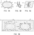
- FIG. 5A is a plan view showing a wiring substrate 1c according to a third embodiment of the present invention.
- FIGS. 5B and 5C are perspective views showing a punch P3 and a die D3 used in a blanking step for manufacture of the wiring substrate 1c.
- FIG. 5D is a partial schematic view showing the blanking step for obtaining the wiring substrate 1c.
- the above-described electrode pads 6 and 7 are not illustrated.
- the wiring substrate 1c includes a substrate body 2c composed of a plurality of ceramic layers c1 to c3 which are similar to the above-described ceramic layers c1 to c3 and stacked together or a single ceramic layer.
- the substrate body 2c has an elongated-circular front surface 3c and an elongated-circular back surface 4c located on opposite sides thereof, and a side surface located between the circumferences of the front surface 3c and the back surface 4c.
- the side surface is composed of two (left and right) curved portions R5, four straight portions 5, and two (upper and lower) shallow concave portions 35.
- the curved portions R5 are disposed at positions which are point symmetry with one another with respect to the center of symmetry of the front surface 3c, the four straight portions 5 are disposed between the two curved portions R5 to be point symmetry with one another with respect to the center of symmetry.
- One of the concave portions 35 is located between the upper straight portions 5, and the other concave portion 35 is located between the lower straight portions 5.
- each of the four straight portions 5 is located on an imaginary elongated circle (an imaginary product outline) S3.
- a mother substrate Gn which is similar to the above-described mother substrate and which has a front surface 3C and a back surface 4C on the opposite sides thereof is prepared beforehand.
- a blanking process is performed, through use of a punch P3 and a die D3 which will be described below, at each of positions along an imaginary elongated circle (imaginary product outline) S3 previously set at each of predetermined positions.
- the positions along the imaginary ellipse S3 are point symmetry with one another with respect to the center of symmetry of the imaginary elongated circle S3.
- the punch P3 has a concave curved surface r5 which is similar in shape to the curved portion R5 and extends from its distal end surface.
- the die D3 has a convex curved surface r5 which is similar in shape to the curved portion R5 and extends from its distal end surface.
- the punch P2 has a distal end surface 31 having three straight sides (specifically, one long straight side and two short straight sides) and a curved side located between the two short straight sides and corresponding to the concave curved surface r5 which is similar in shape to the curved portion R5.
- the die D3 has a receiving hole 32 which is similar in shape to the distal end surface 31 and which includes, as a portion of its inner wall surface, a convex curved surface r5 which is similar in shape to the curved portion R5.
- a punch 36 which has a rectangular distal end surface as in the case of the above-described punch 15 and a die 36 which has a rectangular receiving hole as in the case of the above-described die 16 are prepared seprately.
- the die D3 is disposed on the back surface 4C side of the mother substrate Gn.
- the punch P3 is moved downward on the front surface 3B side of the mother substrate Gn such that the distal end portion of the punch P3 penetrates the mother substrate Gn and enters the receiving hole 32 of the die D3.
- this blanking process may be performed simultaneously at the above-described two positions or performed sequentially position by position.
- the blanking process for forming the curved portions R5 be performed sequentially position by position.
- two through holes 34 which are similar in shape to the distal end surface 31 of the punch P3 and the receiving hole 32 of the die D3 are formed at positions which are located along the elongated circle S3 set on the mother substrate Gn and are point symmetry with one another with respect to the center of symmetry within the elongated circle S3.
- a portion of the inner wall surface of each through hole 34 located on the elongated circle S3 side includes a corresponding one of the curved portions R5.
- the blanking step as described above is performed for each of the plurality of elongated circles S3 set on the mother substrate Gn.
- a blanking process different from the above-described blanking process is performed through use of the punch 36 and the die 37 which are oriented such that their long sides extend along the above-mentioned upper and lower sides.
- a through hole 38 having a rectangular shape in plan view is formed at each of the above-described positions.
- the inner-side long sides of the through holes 38 may coincide with the upper and lower sides of the elongated circle S3.
- the mother substrate Gn having the two through holes 34 and the two through holes 38 formed at desired positions along each elongated circle S3 is fired, and a cutting step similar to the above-described cutting step is then performed along each of imaginary cutting lines located on the outer side of the elongated circle S3 and extending between the curved portions R5 located in the two through holes 34.
- the above-described cutting process may be performed along each of imaginary cutting lines located slightly inward of the elongated circle S3 and extending between the two curved portions R5.
- the straight portions 5 are formed to be located slightly inward of the elongated circle S3.
- the above-described recess 10 may be formed for some or all of the straight portions 5.
- the above-described wiring substrate 1b may have a substrate body 2b having two (left and right) semi-elliptical curved portions as in the case of the above-described wiring substrate 1c.
- a punch and a die similar to the punch P3 and the die D3 may be used.
- the above-described wiring substrate 1c may have a substrate body 2c having four curved portions which are point symmetric with one another.
- a punch and a die similar to the punch P2 and the die D2 may be used.
- ceramic materials other than the above-mentioned alumina e.g., mullite, aluminum nitride, and glass-ceramic
- resins e.g., epoxy resin
- alumina e.g., mullite, aluminum nitride, and glass-ceramic
- resins e.g., epoxy resin
- copper or silver is used for the conductors such as the electrode pads 6 and 7.
- Each of the above-mentioned substrate bodies may be a composite body composed a ceramic insulating layer(s) and a resin insulating layer(s) stacked together.
- Each of the above-mentioned substrate bodies 2a to 2c may have an open cavity or open cavities formed on at least one of the front surface 3a to 3c and the back surface 4a to 4c or an additional through hole(s) extending between the front surface and the back surface.
- each substrate body in plan view so long as the outline is composed of three or more curved portions and three or more straight portions located therebetween, and the total length of the curved portions accounts for at least 40% of the overall length of the side surface of the substrate body as measured in the planar direction thereof.
- the entirety of each substrate body may have a square or rectangular shape, or may have the shape of a regular polygon having five or more corners or a modified polygonal shape.
- the entirety of each substrate body may have a cruciform shape or a star shape.
- the cutting step is performed after firing of the mother substrate Gn.
- the cutting step may be performed before firing of the mother substrate Gn.
- a cutter (not shown) having a straight cutting edge is inserted into the mother substrate Gn before being fired, at each of the above-described positions between the curved portions R1, R4, or R5 located in adjacent ones of the through holes 14, 24, or 34.
- a plurality of straight portions extending in the same direction may be formed simultaneously over a region including the plurality of product outlines set on the mother substrate.
- the above-described recesses may have a semi-circular shape, a semi-elongated circular shape, or a semi-elliptical shape in plan view.
- Each of the recesses may be formed such that it is open outward at an arbitrary position of each curved portion.
- Each of the wiring substrate 1a, 1a', 1a", 1b, and 1c may be a multilayer wiring substrate including two or more ceramic layers.
- the wiring substrate 1a, 1a', 1a", 1b, or 1c has a substrate body composed of two or more ceramic layers stacked together
- blanking is performed, sheet by sheet, for a plurality of green sheets which are to become the plurality of ceramic layers.
- the plurality of green sheets having through holes formed therein are stacked and fired.
- the above-described cutting step may be performed before the plurality of stacked green sheets are fired.
- the present invention makes it possible to provide a wiring substrate which is stable in shape and dimensional accuracy despite that its substrate body formed of an insulating material has a circular shape or the like shape in plan view and a manufacturing method which can reliably manufacture such a wiring substrate by a relatively small number of simple steps.
Landscapes
- Engineering & Computer Science (AREA)
- Manufacturing & Machinery (AREA)
- Microelectronics & Electronic Packaging (AREA)
- Structure Of Printed Boards (AREA)
- Chemical & Material Sciences (AREA)
- Ceramic Engineering (AREA)
- Perforating, Stamping-Out Or Severing By Means Other Than Cutting (AREA)
- Production Of Multi-Layered Print Wiring Board (AREA)
Applications Claiming Priority (1)
| Application Number | Priority Date | Filing Date | Title |
|---|---|---|---|
| JP2018244510A JP7281278B2 (ja) | 2018-12-27 | 2018-12-27 | 配線基板およびその製造方法 |
Publications (2)
| Publication Number | Publication Date |
|---|---|
| EP3675607A2 true EP3675607A2 (de) | 2020-07-01 |
| EP3675607A3 EP3675607A3 (de) | 2020-09-23 |
Family
ID=69061162
Family Applications (1)
| Application Number | Title | Priority Date | Filing Date |
|---|---|---|---|
| EP19219851.3A Withdrawn EP3675607A3 (de) | 2018-12-27 | 2019-12-27 | Verdrahtungssubstrat und verfahren zur herstellung davon |
Country Status (3)
| Country | Link |
|---|---|
| US (1) | US11658082B2 (de) |
| EP (1) | EP3675607A3 (de) |
| JP (1) | JP7281278B2 (de) |
Citations (1)
| Publication number | Priority date | Publication date | Assignee | Title |
|---|---|---|---|---|
| JP2001068599A (ja) | 1999-08-26 | 2001-03-16 | Kyocera Corp | セラミック基板の製造方法 |
Family Cites Families (15)
| Publication number | Priority date | Publication date | Assignee | Title |
|---|---|---|---|---|
| JPS59363B2 (ja) * | 1975-07-25 | 1984-01-06 | 株式会社日立製作所 | セラミツク基板の製造法 |
| GB1553065A (en) * | 1978-01-28 | 1979-09-19 | Int Computers Ltd | Circuit structures including integrated circuits |
| JPH0691628A (ja) * | 1991-11-19 | 1994-04-05 | Ishizuka Glass Co Ltd | セラミックス基板の製造方法 |
| AU2003220901A1 (en) * | 2002-03-29 | 2003-10-13 | Matsushita Electric Industrial Co., Ltd. | Compact self-ballasted fluorescent lamp |
| JP4190555B2 (ja) * | 2006-08-29 | 2008-12-03 | 日本特殊陶業株式会社 | 多数個取り配線基板およびその製造方法 |
| US8018727B2 (en) * | 2006-10-27 | 2011-09-13 | Auto Meter Products, Inc. | Gauge circuit board holding device |
| US7766665B2 (en) * | 2008-01-31 | 2010-08-03 | Ivus Industries, Inc. | Printed circuit board direct connection and method of forming the same |
| JP5077693B2 (ja) * | 2008-08-28 | 2012-11-21 | 東芝ライテック株式会社 | 照明器具 |
| JP5574804B2 (ja) * | 2010-04-27 | 2014-08-20 | 京セラ株式会社 | 多数個取り配線基板 |
| DE102010043220A1 (de) * | 2010-11-02 | 2012-05-03 | Osram Ag | Leuchtvorrichtung und Verfahren zum Zusammenbauen einer Leuchtvorrichtung |
| WO2013054625A1 (ja) * | 2011-10-14 | 2013-04-18 | 株式会社村田製作所 | 部品内蔵樹脂基板 |
| DE102012212025A1 (de) * | 2012-07-10 | 2014-01-16 | Osram Gmbh | Leuchtmodul |
| US8971048B2 (en) * | 2013-03-06 | 2015-03-03 | Alliant Techsystems Inc. | Self-locating electronics package precursor structure, method for configuring an electronics package, and electronics package |
| TWM506378U (zh) | 2014-10-15 | 2015-08-01 | Paragon Sc Lighting Tech Co | 用於提供照明的發光結構及用於承載發光二極體的電路基板 |
| CN110393837B (zh) * | 2018-04-25 | 2022-03-29 | 微邦科技股份有限公司 | 微雾产生器及雾化模块 |
-
2018
- 2018-12-27 JP JP2018244510A patent/JP7281278B2/ja active Active
-
2019
- 2019-12-16 US US16/715,693 patent/US11658082B2/en active Active
- 2019-12-27 EP EP19219851.3A patent/EP3675607A3/de not_active Withdrawn
Patent Citations (1)
| Publication number | Priority date | Publication date | Assignee | Title |
|---|---|---|---|---|
| JP2001068599A (ja) | 1999-08-26 | 2001-03-16 | Kyocera Corp | セラミック基板の製造方法 |
Also Published As
| Publication number | Publication date |
|---|---|
| JP2020107706A (ja) | 2020-07-09 |
| EP3675607A3 (de) | 2020-09-23 |
| US11658082B2 (en) | 2023-05-23 |
| JP7281278B2 (ja) | 2023-05-25 |
| US20200211915A1 (en) | 2020-07-02 |
Similar Documents
| Publication | Publication Date | Title |
|---|---|---|
| KR101536068B1 (ko) | 배선기판, 다수개 취득 배선기판, 및 그 제조방법 | |
| KR102267242B1 (ko) | 적층형 전자부품 및 적층형 전자부품의 제조 방법 | |
| SE524255C2 (sv) | Keramiskt flerskiktssubstrat och förfarande för tillverkning av detsamma | |
| JP4163200B2 (ja) | セラミックパッケージ及びその製造方法、多数個取り用セラミックパッケージ及びその製造方法 | |
| US11658082B2 (en) | Wiring substrate and method of manufacturing the same | |
| JP6819603B2 (ja) | 多層セラミック基板およびその製造方法 | |
| JP2011151281A (ja) | 電子部品の製造方法 | |
| JP5052398B2 (ja) | 多数個取り配線基板および配線基板ならびに電子装置 | |
| JPH03123010A (ja) | 積層電子部品の製造方法 | |
| KR101901777B1 (ko) | 단조에 의한 단자용 금속 부품 제조 방법 및 이에 의해 제조된 단자용 금속 부품 | |
| JP2007109977A (ja) | セラミック基板の製造方法 | |
| JPH0391291A (ja) | 配線基板 | |
| JP3301927B2 (ja) | 分割溝を有するセラミック基板の製造方法 | |
| JP2019047005A (ja) | 多数個取りセラミック基板およびその製造方法 | |
| JP3526527B2 (ja) | セラミック基板 | |
| JP2006128363A (ja) | 多数個取り配線基板および電子装置 | |
| JP2590335Y2 (ja) | 分割溝を有するセラミック基板 | |
| JPH03108506A (ja) | 配線基板の製造方法 | |
| KR20110033607A (ko) | 탄두의 외피 제조방법 | |
| JP2889293B2 (ja) | 焼結板、その製造方法及び製造装置 | |
| JP4034913B2 (ja) | セラミック基板の製造方法 | |
| CN112247227A (zh) | 一种片针中模座组件、夹具体及其加工方法 | |
| WO2023048249A1 (ja) | 電子部品 | |
| JPH02204006A (ja) | スリットプレス金型およびその製造方法 | |
| JP2006289757A (ja) | 配線基板の製造方法およびセラミックグリーンシートの打ち抜き装置 |
Legal Events
| Date | Code | Title | Description |
|---|---|---|---|
| PUAI | Public reference made under article 153(3) epc to a published international application that has entered the european phase |
Free format text: ORIGINAL CODE: 0009012 |
|
| STAA | Information on the status of an ep patent application or granted ep patent |
Free format text: STATUS: THE APPLICATION HAS BEEN PUBLISHED |
|
| AK | Designated contracting states |
Kind code of ref document: A2 Designated state(s): AL AT BE BG CH CY CZ DE DK EE ES FI FR GB GR HR HU IE IS IT LI LT LU LV MC MK MT NL NO PL PT RO RS SE SI SK SM TR |
|
| AX | Request for extension of the european patent |
Extension state: BA ME |
|
| PUAL | Search report despatched |
Free format text: ORIGINAL CODE: 0009013 |
|
| AK | Designated contracting states |
Kind code of ref document: A3 Designated state(s): AL AT BE BG CH CY CZ DE DK EE ES FI FR GB GR HR HU IE IS IT LI LT LU LV MC MK MT NL NO PL PT RO RS SE SI SK SM TR |
|
| AX | Request for extension of the european patent |
Extension state: BA ME |
|
| RIC1 | Information provided on ipc code assigned before grant |
Ipc: H05K 1/03 20060101ALN20200814BHEP Ipc: H05K 3/00 20060101AFI20200814BHEP Ipc: H05K 3/46 20060101ALN20200814BHEP |
|
| STAA | Information on the status of an ep patent application or granted ep patent |
Free format text: STATUS: THE APPLICATION IS DEEMED TO BE WITHDRAWN |
|
| 18D | Application deemed to be withdrawn |
Effective date: 20210324 |