US8971048B2 - Self-locating electronics package precursor structure, method for configuring an electronics package, and electronics package - Google Patents
Self-locating electronics package precursor structure, method for configuring an electronics package, and electronics package Download PDFInfo
- Publication number
- US8971048B2 US8971048B2 US13/787,438 US201313787438A US8971048B2 US 8971048 B2 US8971048 B2 US 8971048B2 US 201313787438 A US201313787438 A US 201313787438A US 8971048 B2 US8971048 B2 US 8971048B2
- Authority
- US
- United States
- Prior art keywords
- electronics package
- branches
- trunk
- circuit
- circuit board
- Prior art date
- Legal status (The legal status is an assumption and is not a legal conclusion. Google has not performed a legal analysis and makes no representation as to the accuracy of the status listed.)
- Active, expires
Links
Images


Classifications
-
- H—ELECTRICITY
- H05—ELECTRIC TECHNIQUES NOT OTHERWISE PROVIDED FOR
- H05K—PRINTED CIRCUITS; CASINGS OR CONSTRUCTIONAL DETAILS OF ELECTRIC APPARATUS; MANUFACTURE OF ASSEMBLAGES OF ELECTRICAL COMPONENTS
- H05K1/00—Printed circuits
- H05K1/02—Details
- H05K1/14—Structural association of two or more printed circuits
- H05K1/148—Arrangements of two or more hingeably connected rigid printed circuit boards, i.e. connected by flexible means
-
- F—MECHANICAL ENGINEERING; LIGHTING; HEATING; WEAPONS; BLASTING
- F42—AMMUNITION; BLASTING
- F42C—AMMUNITION FUZES; ARMING OR SAFETY MEANS THEREFOR
- F42C15/00—Arming-means in fuzes; Safety means for preventing premature detonation of fuzes or charges
- F42C15/40—Arming-means in fuzes; Safety means for preventing premature detonation of fuzes or charges wherein the safety or arming action is effected electrically
-
- F—MECHANICAL ENGINEERING; LIGHTING; HEATING; WEAPONS; BLASTING
- F42—AMMUNITION; BLASTING
- F42C—AMMUNITION FUZES; ARMING OR SAFETY MEANS THEREFOR
- F42C19/00—Details of fuzes
- F42C19/02—Fuze bodies; Fuze housings
-
- F—MECHANICAL ENGINEERING; LIGHTING; HEATING; WEAPONS; BLASTING
- F42—AMMUNITION; BLASTING
- F42C—AMMUNITION FUZES; ARMING OR SAFETY MEANS THEREFOR
- F42C19/00—Details of fuzes
- F42C19/06—Electric contact parts specially adapted for use with electric fuzes
-
- H—ELECTRICITY
- H05—ELECTRIC TECHNIQUES NOT OTHERWISE PROVIDED FOR
- H05K—PRINTED CIRCUITS; CASINGS OR CONSTRUCTIONAL DETAILS OF ELECTRIC APPARATUS; MANUFACTURE OF ASSEMBLAGES OF ELECTRICAL COMPONENTS
- H05K1/00—Printed circuits
- H05K1/02—Details
- H05K1/14—Structural association of two or more printed circuits
- H05K1/144—Stacked arrangements of planar printed circuit boards
-
- H—ELECTRICITY
- H05—ELECTRIC TECHNIQUES NOT OTHERWISE PROVIDED FOR
- H05K—PRINTED CIRCUITS; CASINGS OR CONSTRUCTIONAL DETAILS OF ELECTRIC APPARATUS; MANUFACTURE OF ASSEMBLAGES OF ELECTRICAL COMPONENTS
- H05K2201/00—Indexing scheme relating to printed circuits covered by H05K1/00
- H05K2201/04—Assemblies of printed circuits
- H05K2201/042—Stacked spaced PCBs; Planar parts of folded flexible circuits having mounted components in between or spaced from each other
-
- H—ELECTRICITY
- H05—ELECTRIC TECHNIQUES NOT OTHERWISE PROVIDED FOR
- H05K—PRINTED CIRCUITS; CASINGS OR CONSTRUCTIONAL DETAILS OF ELECTRIC APPARATUS; MANUFACTURE OF ASSEMBLAGES OF ELECTRICAL COMPONENTS
- H05K2201/00—Indexing scheme relating to printed circuits covered by H05K1/00
- H05K2201/04—Assemblies of printed circuits
- H05K2201/046—Planar parts of folded PCBs making an angle relative to each other
-
- H—ELECTRICITY
- H05—ELECTRIC TECHNIQUES NOT OTHERWISE PROVIDED FOR
- H05K—PRINTED CIRCUITS; CASINGS OR CONSTRUCTIONAL DETAILS OF ELECTRIC APPARATUS; MANUFACTURE OF ASSEMBLAGES OF ELECTRICAL COMPONENTS
- H05K2201/00—Indexing scheme relating to printed circuits covered by H05K1/00
- H05K2201/04—Assemblies of printed circuits
- H05K2201/047—Box-like arrangements of PCBs
-
- H—ELECTRICITY
- H05—ELECTRIC TECHNIQUES NOT OTHERWISE PROVIDED FOR
- H05K—PRINTED CIRCUITS; CASINGS OR CONSTRUCTIONAL DETAILS OF ELECTRIC APPARATUS; MANUFACTURE OF ASSEMBLAGES OF ELECTRICAL COMPONENTS
- H05K2201/00—Indexing scheme relating to printed circuits covered by H05K1/00
- H05K2201/05—Flexible printed circuits [FPCs]
- H05K2201/053—Tails
-
- H—ELECTRICITY
- H05—ELECTRIC TECHNIQUES NOT OTHERWISE PROVIDED FOR
- H05K—PRINTED CIRCUITS; CASINGS OR CONSTRUCTIONAL DETAILS OF ELECTRIC APPARATUS; MANUFACTURE OF ASSEMBLAGES OF ELECTRICAL COMPONENTS
- H05K2201/00—Indexing scheme relating to printed circuits covered by H05K1/00
- H05K2201/20—Details of printed circuits not provided for in H05K2201/01 - H05K2201/10
- H05K2201/2036—Permanent spacer or stand-off in a printed circuit or printed circuit assembly
-
- H—ELECTRICITY
- H05—ELECTRIC TECHNIQUES NOT OTHERWISE PROVIDED FOR
- H05K—PRINTED CIRCUITS; CASINGS OR CONSTRUCTIONAL DETAILS OF ELECTRIC APPARATUS; MANUFACTURE OF ASSEMBLAGES OF ELECTRICAL COMPONENTS
- H05K3/00—Apparatus or processes for manufacturing printed circuits
- H05K3/46—Manufacturing multilayer circuits
- H05K3/4688—Composite multilayer circuits, i.e. comprising insulating layers having different properties
- H05K3/4691—Rigid-flexible multilayer circuits comprising rigid and flexible layers, e.g. having in the bending regions only flexible layers
Definitions
- Embodiments of the present disclosure relate to packaging of electronic components and methods of assembly of such packaging. More particularly, embodiments of the present disclosure relate to packaging employing a self-locating electronics package precursor structure, a method of producing an electronics package, and an electronics package which may be suited for miniaturized applications including, without limitation, application to electronic safe and arm assemblies for munitions.
- the present disclosure comprises an electronics package, the electronics package comprising a number of mutually parallel, vertically spaced circuit boards and a flex circuit comprising a trunk extending circumferentially and including a same number of branches as the number of circuit boards, each branch mechanically and electrically connected to one of the number of circuit boards.
- the present disclosure comprises an electronics package precursor structure, the precursor structure including a flex circuit having a linear trunk, a first pair of opposing branches extending perpendicular to the trunk, each branch of the first pair mechanically and electrically connected to a generally circular circuit board, and a second pair of opposing branches extending perpendicular to the trunk, each branch of the second pair mechanically and electrically connected to a generally circular circuit board.
- the present disclosure comprises a method of producing an electronics package, the method comprising providing a generally planar assembly comprising a flex circuit including a linear trunk, a first pair of opposing branches extending perpendicular to the trunk, each branch of the first pair mechanically and electrically connected to a generally circular circuit board and a second pair of opposing branches extending perpendicular to the trunk, each branch of the second pair mechanically and electrically connected to a generally circular circuit board, moving circuit boards connected to the first pair of branches toward one another to a position perpendicular to the plane of the assembly and rotating the circuit boards connected to the first pair of branches along an axis of the linear trunk to a position between the second pair of branches, and moving circuit boards connected to the second pair of branches toward one another to a position perpendicular to the plane of the assembly and on opposing sides of the circuit boards connected to the first pair of branches to place all of the circuit boards in aligned, mutually parallel relationship.
- FIG. 1 is a perspective view of an embodiment of an electronics package of the present disclosure including installed active and passive electronic components;
- FIG. 2 is a perspective view of a precursor structure of the electronics package of the present disclosure including installed active and passive electronic components prior to configuration as the electronics package;
- FIG. 3 is a perspective view of the embodiment of an electronics package of the present disclosure of FIG. 1 , but without electronic components illustrated thereon;
- FIG. 4 is a plan view of elements of the precursor structure of the electronics package of the present disclosure without electronic components prior to configuration as the electronics package of FIG. 3 ;
- FIG. 5A is a top elevation of the embodiment of FIG. 3 ;
- FIG. 5B is a first side elevation of the embodiment of FIG. 3 ;
- FIG. 5C is a second side elevation of the embodiment of FIG. 3 , rotated 90° from FIG. 5B ;
- FIG. 6 is a cross-section of the electronics package of FIG. 3 , taken through line 6 - 6 of FIG. 5A ;
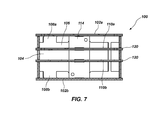
- FIG. 7 is a cross-section of the electronics package of FIG. 3 , taken through line 7 - 7 of FIG. 5A .
- Electronics package 100 comprises a number of circuit boards bearing one or more levels of circuit traces for connection of electronic components thereto, and mechanically and electrically connected to circuit traces of a multi-arm flex circuit, to which a number of baffles are secured. Circuit traces are not depicted for clarity of illustration of the disclosure, and because the number, type and routing of circuit traces are not material to implementation of embodiments of the disclosure.
- electronics package precursor structure 100 ′ comprises first and second outer, generally circular circuit boards 102 a and 102 b mechanically and electrically connected to linear branches 108 a and 108 b extending perpendicularly from linear trunk 106 of flex circuit 104 .
- First and second inner, generally circular circuit boards 110 a and 110 b are mechanically and electrically connected to linear branches 112 a and 112 b extending perpendicularly from trunk 106 of flex circuit 104 and longitudinally offset down trunk 106 from branches 108 a and 108 b .
- baffles 114 of equal length are secured to trunk 106 of flex circuit 104 at equally spaced intervals, and are oriented perpendicular to trunk 106 and parallel to branches 108 a , 108 b , 112 a and 112 b .
- Each baffle 114 includes a recess 116 at each end, and two spaced slots 118 between the ends.
- Recesses 116 of each baffle 114 are longitudinally aligned in a direction parallel to trunk 106 with similarly located recesses of the other baffles 114 , and slots 118 are likewise longitudinally aligned in a direction parallel to trunk 106 with similarly located slots 118 of the other baffles 114 .
- Circuit boards 102 a , 102 b , 110 a and 110 b are of substantially the same dimensions and configuration, with each circuit board 102 a , 102 b , 110 a and 110 b having four circumferentially spaced tabs 120 extending laterally (e.g., radially) therefrom in a major plane of a respective circuit board 102 a , 102 b , 110 a and 110 b from which such tabs 120 extend.
- One or more of circuit boards 102 a , 102 b , 110 a and 110 b may have electronic components mounted thereto on one of both sides, and outer circuit boards 110 a , 110 b may or may not have electronic components exposed on their outer surfaces when electronics package 100 is in an assembled state.
- generally circular circuit board means and includes not only circular circuit boards, but circuit boards of a shape approximating a circle such as polygonal boards (i.e., hexagon, octagon) as well as other circuit board shapes such as, for example, ellipses and ovals.
- Tabs 120 are spaced circumferentially about each respective circuit board 102 a , 102 b , 110 a and 110 b a distance substantially equal to spacing between aligned recesses 116 and aligned slots 118 , as taken in a direction parallel to trunk 106 , the reason for such relationship being described in more detail below with respect to assembly of electronics package 100 .
- electronics package 100 When in an assembled state, as depicted in FIGS. 1 , 3 and 5 A through 7 , electronics package 100 is configured as a stack of vertically spaced, mutually parallel circuit boards, comprising from top to bottom (such terms being used arbitrarily for the sake of convenience of description) circuit board 102 a , circuit board 110 a , circuit board 110 b and circuit board 102 b .
- the tabs 120 of outer circuit boards 102 a and 102 b are received in recesses 116 of baffles 114
- the tabs 120 of inner circuit boards 110 a and 110 b are received in slots 118 of baffles 114
- baffles 114 being spaced around a circumference of assembled electronics package 100 at 90° intervals and oriented perpendicular to circuit boards 110 a , 102 a , 102 b and 110 b
- Trunk 106 of flex circuit 104 wraps circumferentially about electronics package 100 in a direction parallel to circuit boards 110 a , 102 a , 102 b and 110 b .
- branches 112 a and 112 b of flex circuit 104 respectively bend from adjacent trunk 106 upward and downward perpendicularly to form a loop L inward of the circumference of electronics package 100 , reverse direction and then bend at B to extend into the plane of inner circuit boards 110 a and 110 b to which they are respectively attached.
- branches 108 a and 108 b of flex circuit 104 bend from adjacent trunk 106 perpendicularly into the plane of outer circuit boards 102 a and 102 b to which they are respectively attached.
- Extensions 122 a and 122 b of branches 108 a and 108 b comprise flex tabs 124 a and 124 b ( FIG.
- each outer circuit board 102 a and 102 b from a connection of a respective branch 108 a and 108 b to trunk 106 wrap toward each other and may be adhesively bonded to an exterior surface of trunk 106 of flex circuit 104 , taped together, or otherwise mutually secured.
- At least one of the circuit boards may comprise a laminate, and the flex circuit branch connected thereto may extend between members of the laminate circuit board ( FIGS. 6 and 7 ).
- Electronics package 100 may, in its configured state, be characterized in shape as a generally right circular cylinder.
- Connections to external circuitry may be effected from outer circuit boards 102 a or 102 b , and, if desired, one or both extensions 122 a and 122 b may be elongated for connection at ends thereof, as is known in the flex circuit art to those of ordinary skill.
- the manner of effecting external electrical connections is by way of illustration and not limitation.
- inner circuit boards 110 a and 110 b are folded upward toward one another and perpendicular to the plane of trunk 106 of flex circuit 104 , tabs 120 inserted into slots 118 of the lowermost two baffles 114 as branches 112 a and 112 b flex to form loops L and bends B ( FIG.
- a length of shrink fit tubing may be applied around electronics package 100 and heated to shrink about electronics package 100 to insulate the electronics package 100 from a housing that may receive it or to firm up the assembly.
- the assembly comprising electronics package 100 may be potted in a dielectric material to harden the electronics, such a technique being known to those of ordinary skill in the art.
- the electronics package of the present disclosure may be adaptable to miniaturization, and in one embodiment component parts thereof may be fabricated and assembled into a package smaller than one cubic inch, although the present disclosure is not limited by package dimensions.
- the electronics package may be employed, with appropriate active and passive electronic components, in a warhead of a self-propelled projectile such as may be employed in defense of an aerospace vehicle against airborne threats.
- the electronics package may find application to general purpose, miniaturized electronics packaging.
- the present disclosure may, in some embodiments, employ conventional printed circuit board (also known as printed wiring board) and flex circuit technology with self-locating features to provide structural stability and high density packaging.
- printed circuit board also known as printed wiring board
- flex circuit technology with self-locating features to provide structural stability and high density packaging.
Landscapes
- Engineering & Computer Science (AREA)
- General Engineering & Computer Science (AREA)
- Microelectronics & Electronic Packaging (AREA)
- Combinations Of Printed Boards (AREA)
- Structures For Mounting Electric Components On Printed Circuit Boards (AREA)
Abstract
Description
Claims (16)
Priority Applications (2)
| Application Number | Priority Date | Filing Date | Title |
|---|---|---|---|
| US13/787,438 US8971048B2 (en) | 2013-03-06 | 2013-03-06 | Self-locating electronics package precursor structure, method for configuring an electronics package, and electronics package |
| PCT/US2014/017274 WO2014137604A2 (en) | 2013-03-06 | 2014-02-20 | Self-locating electronics package precursor structure, method for configuring an electronics package, and electronics package |
Applications Claiming Priority (1)
| Application Number | Priority Date | Filing Date | Title |
|---|---|---|---|
| US13/787,438 US8971048B2 (en) | 2013-03-06 | 2013-03-06 | Self-locating electronics package precursor structure, method for configuring an electronics package, and electronics package |
Publications (2)
| Publication Number | Publication Date |
|---|---|
| US20140254109A1 US20140254109A1 (en) | 2014-09-11 |
| US8971048B2 true US8971048B2 (en) | 2015-03-03 |
Family
ID=50277319
Family Applications (1)
| Application Number | Title | Priority Date | Filing Date |
|---|---|---|---|
| US13/787,438 Active 2033-06-09 US8971048B2 (en) | 2013-03-06 | 2013-03-06 | Self-locating electronics package precursor structure, method for configuring an electronics package, and electronics package |
Country Status (2)
| Country | Link |
|---|---|
| US (1) | US8971048B2 (en) |
| WO (1) | WO2014137604A2 (en) |
Cited By (3)
| Publication number | Priority date | Publication date | Assignee | Title |
|---|---|---|---|---|
| US20140293531A1 (en) * | 2013-03-27 | 2014-10-02 | Hewlett-Packard Development Company, L.P. | Server node |
| US12349302B2 (en) * | 2021-11-26 | 2025-07-01 | Stmicroelectronics S.R.L. | Electronic module carrying a plurality of electronic devices |
| US12442701B2 (en) | 2020-03-04 | 2025-10-14 | Brp Megatech Industries Inc. | Structural locating sensors for a sensor module using a printed circuit board assembly |
Families Citing this family (5)
| Publication number | Priority date | Publication date | Assignee | Title |
|---|---|---|---|---|
| DE102017103704A1 (en) * | 2017-02-23 | 2018-08-23 | Turck Holding Gmbh | Measuring instrument for process measuring technology |
| KR102030824B1 (en) * | 2017-11-01 | 2019-10-10 | 현대오트론 주식회사 | Electronic control device |
| CN108482149A (en) * | 2018-03-22 | 2018-09-04 | 普汽新能(北京)科技有限公司 | A method of assembling batteries of electric automobile group with high-low pressure integrated circuit board |
| JP7281278B2 (en) * | 2018-12-27 | 2023-05-25 | 日本特殊陶業株式会社 | Wiring board and its manufacturing method |
| CN113507777B (en) * | 2021-09-09 | 2021-11-16 | 南通海舟电子科技有限公司 | Heat dissipation printed circuit board for non-planar installation and installation method thereof |
Citations (14)
| Publication number | Priority date | Publication date | Assignee | Title |
|---|---|---|---|---|
| US3676746A (en) * | 1970-12-23 | 1972-07-11 | Honeywell Inf Systems | Compatible modular circuit board connector |
| US6167809B1 (en) | 1998-11-05 | 2001-01-02 | The United States Of America As Represented By The Secretary Of The Army | Ultra-miniature, monolithic, mechanical safety-and-arming (S&A) device for projected munitions |
| US6431071B1 (en) | 2000-09-18 | 2002-08-13 | Trw Inc. | Mems arm fire and safe and arm devices |
| US7444937B2 (en) | 2005-10-27 | 2008-11-04 | Giat Industries | Pyrotechnic safety device with micro-machined barrier |
| US7490553B2 (en) | 2005-10-27 | 2009-02-17 | Giat Industries | Pyrotechnic safety device of reduced dimensions |
| DE102007046493A1 (en) | 2007-09-28 | 2009-04-09 | Continental Automotive Gmbh | Three-dimensional electronic circuit carrier structure, as well as circuit base carrier having the circuit carrier structure as a functional component and three-dimensional circuit arrangement consisting of at least two such three-dimensional circuit carrier structures |
| DE102008025938A1 (en) | 2008-05-30 | 2009-12-03 | Continental Automotive Gmbh | Printed circuit board arrangement for control unit of internal combustion engine of motor vehicle, has plug connectors conductive coupled with related rigid regions and positioned adjacent to one another to form common plug connector unit |
| US20100008034A1 (en) | 2008-07-14 | 2010-01-14 | International Business Machines Corporation | Tubular memory module |
| DE202011003115U1 (en) | 2011-02-23 | 2011-05-05 | CCS Technology, Inc., Wilmington | Test connection device for a data socket |
| US8276515B1 (en) | 2008-05-01 | 2012-10-02 | The United States Of America As Represented By The Secretary Of The Army | Ultra-miniature electro-mechanical safety and arming device |
| DE202012006289U1 (en) | 2012-06-06 | 2012-10-09 | Power Mate Technology Co., Ltd. | Miniaturized voltage conversion device |
| US8342717B1 (en) | 2007-05-21 | 2013-01-01 | Goldeneye, Inc. | Foldable LEDs light recycling cavity |
| US20130008334A1 (en) | 2010-03-16 | 2013-01-10 | Qinetiq Limited | Mems detonator |
| US20140160683A1 (en) * | 2006-08-18 | 2014-06-12 | Delphi Technologies, Inc. | Lightweight audio system for automotive applications and method |
-
2013
- 2013-03-06 US US13/787,438 patent/US8971048B2/en active Active
-
2014
- 2014-02-20 WO PCT/US2014/017274 patent/WO2014137604A2/en not_active Ceased
Patent Citations (16)
| Publication number | Priority date | Publication date | Assignee | Title |
|---|---|---|---|---|
| US3676746A (en) * | 1970-12-23 | 1972-07-11 | Honeywell Inf Systems | Compatible modular circuit board connector |
| US6167809B1 (en) | 1998-11-05 | 2001-01-02 | The United States Of America As Represented By The Secretary Of The Army | Ultra-miniature, monolithic, mechanical safety-and-arming (S&A) device for projected munitions |
| US6431071B1 (en) | 2000-09-18 | 2002-08-13 | Trw Inc. | Mems arm fire and safe and arm devices |
| US7444937B2 (en) | 2005-10-27 | 2008-11-04 | Giat Industries | Pyrotechnic safety device with micro-machined barrier |
| US7490553B2 (en) | 2005-10-27 | 2009-02-17 | Giat Industries | Pyrotechnic safety device of reduced dimensions |
| US20140160683A1 (en) * | 2006-08-18 | 2014-06-12 | Delphi Technologies, Inc. | Lightweight audio system for automotive applications and method |
| US8342717B1 (en) | 2007-05-21 | 2013-01-01 | Goldeneye, Inc. | Foldable LEDs light recycling cavity |
| DE102007046493A1 (en) | 2007-09-28 | 2009-04-09 | Continental Automotive Gmbh | Three-dimensional electronic circuit carrier structure, as well as circuit base carrier having the circuit carrier structure as a functional component and three-dimensional circuit arrangement consisting of at least two such three-dimensional circuit carrier structures |
| US8276515B1 (en) | 2008-05-01 | 2012-10-02 | The United States Of America As Represented By The Secretary Of The Army | Ultra-miniature electro-mechanical safety and arming device |
| DE102008025938A1 (en) | 2008-05-30 | 2009-12-03 | Continental Automotive Gmbh | Printed circuit board arrangement for control unit of internal combustion engine of motor vehicle, has plug connectors conductive coupled with related rigid regions and positioned adjacent to one another to form common plug connector unit |
| US20100008034A1 (en) | 2008-07-14 | 2010-01-14 | International Business Machines Corporation | Tubular memory module |
| US20130008334A1 (en) | 2010-03-16 | 2013-01-10 | Qinetiq Limited | Mems detonator |
| DE202011003115U1 (en) | 2011-02-23 | 2011-05-05 | CCS Technology, Inc., Wilmington | Test connection device for a data socket |
| GB2488422B (en) | 2011-02-23 | 2014-08-27 | Ccs Technology Inc | Test connection apparatus for a data jack |
| DE202012006289U1 (en) | 2012-06-06 | 2012-10-09 | Power Mate Technology Co., Ltd. | Miniaturized voltage conversion device |
| US20130328543A1 (en) | 2012-06-06 | 2013-12-12 | Lien-Hsing Chen | Miniaturize voltage-transforming device |
Non-Patent Citations (2)
| Title |
|---|
| PCT International Search Report, ISA/EP, International Application No. PCT/US2014/017274, Oct. 24, 2014, five (5) pages. |
| Written Opinion of the International Searching Authority, ISA/EP, International Application No. PCT/US2014/017274, Oct. 24, 2014, six (6) pages. |
Cited By (3)
| Publication number | Priority date | Publication date | Assignee | Title |
|---|---|---|---|---|
| US20140293531A1 (en) * | 2013-03-27 | 2014-10-02 | Hewlett-Packard Development Company, L.P. | Server node |
| US12442701B2 (en) | 2020-03-04 | 2025-10-14 | Brp Megatech Industries Inc. | Structural locating sensors for a sensor module using a printed circuit board assembly |
| US12349302B2 (en) * | 2021-11-26 | 2025-07-01 | Stmicroelectronics S.R.L. | Electronic module carrying a plurality of electronic devices |
Also Published As
| Publication number | Publication date |
|---|---|
| WO2014137604A2 (en) | 2014-09-12 |
| WO2014137604A3 (en) | 2014-12-31 |
| US20140254109A1 (en) | 2014-09-11 |
Similar Documents
| Publication | Publication Date | Title |
|---|---|---|
| US8971048B2 (en) | Self-locating electronics package precursor structure, method for configuring an electronics package, and electronics package | |
| US9601842B2 (en) | Connecting unit having a column with a plurality of planar elastic fins extending from the column | |
| CN107148383B (en) | Unmanned aerial vehicle rack and unmanned aerial vehicle | |
| US9324491B2 (en) | Inductor device and electronic apparatus | |
| RU2016104882A (en) | SHOT PUNCH SYSTEM AND COMPONENTS | |
| US9648746B2 (en) | Composite electronic component and board having the same | |
| US20150003839A1 (en) | Optical transceiver | |
| EP2963742A1 (en) | Rotary connector | |
| JP6160308B2 (en) | Laminated board | |
| CN106486268A (en) | Coil device | |
| JP2017537461A (en) | Interconnect transition equipment | |
| US11432448B2 (en) | Method of forming an electronic device | |
| US20130025924A1 (en) | Lead component holder and electronic device | |
| US20130215580A1 (en) | Magnetic assembly | |
| JP6693707B2 (en) | Substrate integrated interconnect | |
| JP3206832U (en) | Electronic device package case | |
| EP3407688B1 (en) | Method of assembling a circuit card assembly | |
| US20150294777A1 (en) | Induction Component | |
| JP6583560B2 (en) | Electronics | |
| WO2011065361A1 (en) | Connecting member | |
| US10460872B2 (en) | Electronic device | |
| JP2021057487A (en) | Film capacitor | |
| US10797290B2 (en) | Assembly of electronic components | |
| US20140036414A1 (en) | Capacitor | |
| US20200219666A1 (en) | Power storage module |
Legal Events
| Date | Code | Title | Description |
|---|---|---|---|
| AS | Assignment |
Owner name: ALLIANT TECHSYSTEMS INC., VIRGINIA Free format text: ASSIGNMENT OF ASSIGNORS INTEREST;ASSIGNORS:LUCAS, JAMES D.;MCKELLIPS, CHRISTOPHER A.;REEL/FRAME:029935/0624 Effective date: 20130306 |
|
| AS | Assignment |
Owner name: BANK OF AMERICA, N.A., CALIFORNIA Free format text: INTELLECTUAL PROPERTY SECURITY AGREEMENT SUPPLEMENT;ASSIGNOR:ALLIANT TECHSYSTEMS INC.;REEL/FRAME:030426/0757 Effective date: 20130331 |
|
| FEPP | Fee payment procedure |
Free format text: PAYOR NUMBER ASSIGNED (ORIGINAL EVENT CODE: ASPN); ENTITY STATUS OF PATENT OWNER: LARGE ENTITY |
|
| AS | Assignment |
Owner name: BANK OF AMERICA, N.A., CALIFORNIA Free format text: SECURITY AGREEMENT;ASSIGNORS:ALLIANT TECHSYSTEMS INC.;CALIBER COMPANY;EAGLE INDUSTRIES UNLIMITED, INC.;AND OTHERS;REEL/FRAME:031731/0281 Effective date: 20131101 |
|
| STCF | Information on status: patent grant |
Free format text: PATENTED CASE |
|
| AS | Assignment |
Owner name: ORBITAL ATK, INC., VIRGINIA Free format text: CHANGE OF NAME;ASSIGNOR:ALLIANT TECHSYSTEMS INC.;REEL/FRAME:035753/0373 Effective date: 20150209 |
|
| AS | Assignment |
Owner name: WELLS FARGO BANK, NATIONAL ASSOCIATION, AS ADMINISTRATIVE AGENT, NORTH CAROLINA Free format text: SECURITY AGREEMENT;ASSIGNORS:ORBITAL ATK, INC.;ORBITAL SCIENCES CORPORATION;REEL/FRAME:036732/0170 Effective date: 20150929 Owner name: WELLS FARGO BANK, NATIONAL ASSOCIATION, AS ADMINIS Free format text: SECURITY AGREEMENT;ASSIGNORS:ORBITAL ATK, INC.;ORBITAL SCIENCES CORPORATION;REEL/FRAME:036732/0170 Effective date: 20150929 |
|
| AS | Assignment |
Owner name: ORBITAL ATK, INC. (F/K/A ALLIANT TECHSYSTEMS INC.), VIRGINIA Free format text: RELEASE BY SECURED PARTY;ASSIGNOR:BANK OF AMERICA, N.A.;REEL/FRAME:036816/0624 Effective date: 20150929 Owner name: AMMUNITION ACCESSORIES, INC., ALABAMA Free format text: RELEASE BY SECURED PARTY;ASSIGNOR:BANK OF AMERICA, N.A.;REEL/FRAME:036816/0624 Effective date: 20150929 Owner name: FEDERAL CARTRIDGE CO., MINNESOTA Free format text: RELEASE BY SECURED PARTY;ASSIGNOR:BANK OF AMERICA, N.A.;REEL/FRAME:036816/0624 Effective date: 20150929 Owner name: EAGLE INDUSTRIES UNLIMITED, INC., MISSOURI Free format text: RELEASE BY SECURED PARTY;ASSIGNOR:BANK OF AMERICA, N.A.;REEL/FRAME:036816/0624 Effective date: 20150929 Owner name: ORBITAL ATK, INC. (F/K/A ALLIANT TECHSYSTEMS INC.) Free format text: RELEASE BY SECURED PARTY;ASSIGNOR:BANK OF AMERICA, N.A.;REEL/FRAME:036816/0624 Effective date: 20150929 Owner name: ALLIANT TECHSYSTEMS INC., VIRGINIA Free format text: RELEASE BY SECURED PARTY;ASSIGNOR:BANK OF AMERICA, N.A.;REEL/FRAME:036816/0624 Effective date: 20150929 |
|
| AS | Assignment |
Owner name: ORBITAL ATK, INC., VIRGINIA Free format text: TERMINATION AND RELEASE OF SECURITY INTEREST IN PATENTS;ASSIGNOR:WELLS FARGO BANK, NATIONAL ASSOCIATION, AS ADMINISTRATIVE AGENT;REEL/FRAME:046477/0874 Effective date: 20180606 |
|
| MAFP | Maintenance fee payment |
Free format text: PAYMENT OF MAINTENANCE FEE, 4TH YEAR, LARGE ENTITY (ORIGINAL EVENT CODE: M1551); ENTITY STATUS OF PATENT OWNER: LARGE ENTITY Year of fee payment: 4 |
|
| AS | Assignment |
Owner name: NORTHROP GRUMMAN INNOVATION SYSTEMS, INC., MINNESOTA Free format text: CHANGE OF NAME;ASSIGNOR:ORBITAL ATK, INC.;REEL/FRAME:047400/0381 Effective date: 20180606 Owner name: NORTHROP GRUMMAN INNOVATION SYSTEMS, INC., MINNESO Free format text: CHANGE OF NAME;ASSIGNOR:ORBITAL ATK, INC.;REEL/FRAME:047400/0381 Effective date: 20180606 |
|
| AS | Assignment |
Owner name: NORTHROP GRUMMAN INNOVATION SYSTEMS LLC, MINNESOTA Free format text: CHANGE OF NAME;ASSIGNOR:NORTHROP GRUMMAN INNOVATION SYSTEMS, INC.;REEL/FRAME:055223/0425 Effective date: 20200731 |
|
| AS | Assignment |
Owner name: NORTHROP GRUMMAN SYSTEMS CORPORATION, MINNESOTA Free format text: ASSIGNMENT OF ASSIGNORS INTEREST;ASSIGNOR:NORTHROP GRUMMAN INNOVATION SYSTEMS LLC;REEL/FRAME:055256/0892 Effective date: 20210111 |
|
| MAFP | Maintenance fee payment |
Free format text: PAYMENT OF MAINTENANCE FEE, 8TH YEAR, LARGE ENTITY (ORIGINAL EVENT CODE: M1552); ENTITY STATUS OF PATENT OWNER: LARGE ENTITY Year of fee payment: 8 |